SlideShare ist ein Scribd-Unternehmen logo
1 von 16
What is Digital Electronics
  A description of what we mean by digital electronics is, strangely, best approached from
a description of what it is not. It is not analogue. Analogue electronics are designed and
used to process analogue signals. An analogue signal is a fluctuating voltage which can
have any numerical value. i.e it may be tiny fractions of a volt or it may be hundreds of
volts. It may be a constant voltage or rapidly changing. The key feature that separates it
from digital electronics is this ability to assume any value within a continuous range. In
many ways this is a more true reflection of the real world than digital signals. Nnnnext If
you consider the amplification of a singers voice via a microphone it is obvious that the
resulting signal from the microphone will have a voltage continuously varying in
amplitude from the quietest to the loudest note. The processing of this signal must take
account of this to accurately reproduce it when amplified.
   In sharp contrast to this is digital electronics. A digital signal can only have one of two
possible values. The exact value of these voltages depends on the particular type of
digital circuit but one of the most common systems uses +5 volts and 0 volts. In this
system the +5v is referred to as the digital High (or simply HI) and the 0v as digital Low
(or LO). At first glance this may seem a little restrictive. After all what real world signals
can be represented (and then processed) by two states, except perhaps a simple switch
which is either on or off ?
   The true power of digital representation becomes apparent when we start to consider
patterns of these two states rather than just the one. If you take two signals , each capable
of being either HI or LO then the combination can have four different patterns i.e. LO
LO, LO HI, HI LO, HI HI. By considering the pattern rather than just the individual
signal we have increased the range of what can be represented from two to four. Similarly
we can use three digital signals to represent a range of 8 and four signals for a range of
16. More generally, if we use N signals we can represent 2N possible patterns.
   Lets give these patterns a name. Conventionally we use the BINARY number system to
name these patterns of HI and LO, although you should be aware that this is not always
the case. Below you can see a table of the first few binary number patterns. The HI is
represented as '1' and the LO as '0
Using patterns of these "two state" signals we are getting back to the ability that analogue
signals have in representing a bigger range of values. However, representing real world
signals using these discrete values is a bit like using an approximation. It gives you
roughly what you had but not exactly. If we take the example of the singer and the
amplified microphone and assume the microphone signal varied from, say, 0.1 volts to
3.2 volts, then we could use 5 digital signals to represent each 0.1 volt level (i.e. 32
different binary patterns). We could then process this and generate bigger numbers which
could be used to generate correspondingly larger voltages (i.e amplification). The only
thing wrong with this is quality. We would be ignoring, or actually rounding off, the
intermediate values of signal between these discrete values. Trust me on this; the singer
would not sound so good. If however we had used 32 digital signals then the
RESOLUTION of the representation would be much better and, in fact , you would
probably not be able to distinguish the resultant amplified signal from the analogue
processed type.
   The binary representation of real world signals is important, but , by no means, the
only use of digital electronics. In the next section we will look at the use of these
BINARY patterns to represent numbers which are manipulated as numbers without any
requirement to represent an analogue signal. We will also show how these HI/LO patterns
can be used to represent the logical decision making process we all take for granted
Why is digital electronics important to modern technology and information processing?
Digital electronics leads to fewer mistakes in sending and receiving information. Also the
amount of information is greater than when using analogue electronics. Also simple tasks
and basic mathematics become much easier.

The principles of digital electronics

The circuits and components we have discussed are very useful. You can build a radio or
television with them. You can make a telephone. Even if that was all there was to
electronics, it would still be very useful. However, the great breakthrough in the last fifty
years or so has been in digital electronics. This is the subject which gave us the computer.
The computer has revolutionised the way business, engineering and science are done.
Small computers programmed to do a specific job (called microprocessors) are now used
in almost every electronic machine from cars to washing machines. Computers have also
changed the way we communicate. We used to have telegraph or telephone wires passing
up and down a country — each one carrying one telephone call or signal. We now have
optic fibres each capable of carrying tens of thousands of telephone calls using digital
signals.

So, what is a digital signal? Look at Figure 1. A normal signal, called an analogue signal,
carries a smooth wave. At any time, the voltage of the signal could take any value. It
could be 2,00 V or 3,53 V or anything else. A digital signal can only take certain voltages.
The simplest case is shown in the figure — the voltage takes one of two values. It is
either high, or it islow. It never has any other value.

These two special voltages are given symbols. The low voltage level is written 0, while
the high voltage level is written as 1. When you send a digital signal, you set the voltage
you want (0 or 1), then keep this fixed for a fixed amount of time (for example 0.01 μs),
then you send the next 0 or 1. The digital signal in Figure 1 could be written 01100101.


                                Figure 1: The difference between
                                 normal (analogue) signals and
                                      digital signals.


Why are digital signals so good?
Using a computer, any information can be turned into a pattern of 0s and 1s. Pictures,
recorded music, text and motion pictures can all be turned into a string of 0s and 1s and
transmitted or stored in the same way. The computer receiving the signal at the other end
converts it back again. A Compact Disc (CD) for example, can store music or text or
pictures, and all can be read using a computer.

The 0 and the 1 look very different. You can immediately tell if a 0 or a 1 is being sent.
Even if there is interference, you can still tell whether the sender sent a 0 or a 1. This
means that fewer mistakes are made when reading a digital signal. This is why the best
music recording technologies, and the most modern cameras, for example, all use digital
technology.

Using the 0s and 1s you can count, and do all kinds of mathematics. This will be
explained in more detail in the next section.

The simplest digital circuits are called logic gates. Each logic gate makes a decision
based on the information it receives. Different logic gates are set up to make the decisions
in different ways. Each logic gate will be made of many microscopic transistors
connected together within a thin wafer of silicon. This tiny circuit is called an Integrated
Circuit or I.C. - all the parts are in one place (integrated) on the silicon wafer.


.Biodiesel refers to a vegetable oil- or animal fat-based diesel fuel§ consisting of long-
chain alkyl§ (methyl§, propyl§ or ethyl§) esters§. Biodiesel is typically made by
chemically reacting lipids§ (e.g.,vegetable oil§, animal fat (tallow§[1][2])) with an
alcohol§ producing fatty acid esters§.
Biodiesel is meant to be used in standard diesel engines and is thus distinct from the
vegetable and waste oils used to fuel converted diesel engines. Biodiesel can be used
alone, or blended with petrodiesel. Biodiesel can also be used as a low carbon alternative
to heating oil§.
The National Biodiesel Board§ (USA) also has a technical definition of "biodiesel" as a
mono-alkyl ester.[3]
Blends of biodiesel and conventional hydrocarbon-based diesel are products most
commonly distributed for use in the retail diesel fuel marketplace. Much of the world
uses a system known as the "B" factor to state the amount of biodiesel in any fuel mix:[4]
      100% biodiesel is referred to as B100, while
      20% biodiesel, 80% petrodiesel is labeled B20
      5% biodiesel, 95% petrodiesel is labeled B5
      2% biodiesel, 98% petrodiesel is labeled B2.
Blends of 20% biodiesel and lower can be used in diesel equipment with no, or only
minor modifications,[5] although certain manufacturers do not extend warranty coverage
if equipment is damaged by these blends. The B6 to B20 blends are covered by the
ASTM§ D7467 specification.[6] Biodiesel can also be used in its pure form (B100), but
may require certain engine modifications to avoid maintenance and performance
problems.[7] Blending B100 with petroleum diesel may be accomplished by:
     Mixing in tanks at manufacturing point prior to delivery to tanker truck
     Splash mixing in the tanker truck (adding specific percentages of biodiesel and
    petroleum diesel)
     In-line mixing, two components arrive at tanker truck simultaneously.
     Metered pump mixing, petroleum diesel and biodiesel meters are set to X total
    volume, transfer pump pulls from two points and mix is complete on leaving pump
     APPLICATION
Biodiesel can be used in pure form (B100) or may be blended with petroleum diesel at
any concentration in most injection pump diesel engines. New extreme high-pressure
(29,000 psi) common rail§ engines have strict factory limits of B5 or B20, depending on
manufacturer.[citation needed] Biodiesel has different solvent§ properties than
petrodiesel, and will degrade natural rubber§ gaskets§ and hoses§ in vehicles (mostly
vehicles manufactured before 1992), although these tend to wear out naturally and most
likely will have already been replaced with FKM§, which is nonreactive to biodiesel.
Biodiesel has been known to break down deposits of residue in the fuel lines where
petrodiesel has been used.[8] As a result, fuel filters§ may become clogged with
particulates if a quick transition to pure biodiesel is made. Therefore, it is recommended
to change the fuel filters on engines and h
 AVABALITY & PRICE Global biodiesel production§ reached 3.8 million tons in 2005.
Approximately 85% of biodiesel production came from the European Union.[citation
needed]
In 2007, in the United States, average retail (at the pump) prices, including federal and
state fuel taxes§, of B2/B5 were lower than petroleum§ diesel by about 12 cents, and B20
blends were the same as petrodiesel.[42] However, as part as a dramatic shift in diesel
pricing, by July 2009, the US DOE was reporting average costs of B20 15 cents per
gallon higher than petroleum diesel ($2.69/gal vs. $2.54/gal).[43] B99 and B100
generally cost more than petrodiesel except where local governments provide a tax
incentive or subsidy.
BIODIESA; FEED BACK
A variety of oils can be used to produce biodiesel. These include:
    Virgin oil feedstock – rapeseed and soybean oils§ are most commonly used,
   soybean oil alone accounting for about ninety percent of all fuel stocks in the US. It
   also can be obtained from Pongamia§, field pennycress§ and jatropha§ and other
   crops such as mustard§, jojoba§, flax§, sunflower§, palm oil§, coconut§, hemp§ (see
   list of vegetable oils for biofuel§ for more information);
    Waste vegetable oil§ (WVO);
 Animal fats§ including tallow§, lard§, yellow grease§, chicken fat,[56] and the
   by-products of the production of Omega-3 fatty acids§ from fish oil.
    Algae§, which can be grown§ using waste materials such as sewage[57] and
   without displacing land currently used for food production.
    Oil from halophytes§ such as Salicornia bigelovii§, which can be grown using
   saltwater in coastal areas where conventional crops cannot be grown, with yields
   equal to the yields of soybeans and other oilseeds grown using freshwater
   irrigation[58]
   CURRENT RESERCH
There is ongoing research into finding more suitable crops and improving oil yield. Other
sources are possible including human fecal matter, with Ghana§ building its first "fecal
sludge-fed biodiesel plant." [96] Using the current yields, vast amounts of land and fresh
water would be needed to produce enough oil to completely replace fossil fuel usage. It
would require twice the land area of the US to be devoted to soybean production, or two-
thirds to be devoted to rapeseed production, to meet current US heating and
transportation needs.[citation needed]
Specially bred mustard varieties can produce reasonably high oil yields and are very
useful in crop rotation§ with cereals, and have the added benefit that the meal leftover
after the oil has been pressed out can act as an effective and biodegradable pesticide.[97]
The NFESC§, with Santa Barbara§-based Biodiesel Industries is working to develop
biodiesel technologies for the US navy and military, one of the largest diesel fuel users in
the world.[98]
A group of Spanish developers working for a company called Ecofasa§ announced a new
biofuel made from trash. The fuel is created from general urban waste which is treated by
bacteria to produce fatty acids, which can be used to make biodiesel.[99]
Another approach that does not require the use of chemical for the production involves
the use of genetically modified microbes.[100][101]
Sagarika (missile)
[edit§]Development
Development of the K-15 missile started in the late 1990s with the goal of building a
submarine-launched ballistic missile for use with the Indian Navy§ nuclear-powered
Arihant class submarines§.[6][7] Sagarika has a length of 10 metres (33 ft), diameter of
0.74 metres (2 ft 5 in), weighs 17 tonnes and can carry a payload of up to 1,000 kilograms
(2,205 lb) over 700 kilometres (435 mi). It was developed at the DRDO§’s missile
complex in Hyderabad§.[8]
The development of the underwater missile launcher, known as Project 420, was
completed in 2001 and handed over to the Indian Navy§ for trials. The missile launcher is
developed at Hazira in Gujarat§.[9] The Sagarika missile began integration with India's
nuclear-powered§ Arihant class submarine§ that began sea trials on the 26 July 2009.[10]
By 2008, the missile was successfully test fired seven times, and tested to its full range up
to four times. The tests of February 26, 2008, were conducted from a submerged pontoon
50 metres (160 ft) beneath the surface off the coast of Visakhapatnam§.[6][8][11][12] A
land-based version of the K-15 Sagarika was successfully test-fired on November 12,
2008.[13] A full range test of the missile was done on 11 March 2012.[14] The twelfth
and final development trial of the missiles was conducted on 27 January 2013. According
toV.K. Saraswat§, the missile was again tested for its full range of 7
Yesterday India successfully test-fired the underwater ballistic missile, Sagarika K-15
(code-named B05), off the Visakhapatnam coast, marking en end to a series of
developmental trials.
The trail was conducted on a day when China tested a missile defence system, an
interceptor.
K-15 Sagarika is a nuclear-capable submarine-launched ballistic missile with a range of
700 kilometres (435 mi).

In its twelfth flight trial, the 10-metre tall Submarine-Launched Ballistic Missile (SLBM)
lifted off from a pontoon, rose to an altitude of 20 km and reached a distance of about 700
km as it splashed down in the waters of the Bay of Bengal near the pre-designated target
point.
According to scientific advisor to the Defence Minister V.K. Saraswat, the missile was
tested for its full range of 700 km and the mission met all its objectives. He said the
impact accuracy of the medium range strategic missile was in single digit.
With the completion of developmental trials, the process of integrating K-15 missile with
INS Arihant, the indigenously-built nuclear submarine, will begin soon.
As many as 12 nuclear-tipped missiles, each weighing six tonnes will be integrated with
Arihant, which will be powered by an 80 MWt (thermal) reactor that uses enriched
uranium as fuel and light water as coolant and moderator.
India is only the fifth country to have such a missile — the other four nations being the
United States, Russia, France and China.


Read more: Meanwhile the reactor has been integrated with the submarine and it was
expected to go critical in May/ June 2013. Once that was done, the harbour trials will
begin.

Read more:
New Delhi: India’s 700 kms range Sagarika (K-15) submarine launched ballistic missile
(SLBM) tested on 16 March 2012, was unsuccessful.
This was the second test within a span of five days. The first test in the last fortnight, was
carried out on 11 March which was reported to be successful. Both tests took place about
10 kms off Visakhapatam on the east coast of India.
In the absence of a submarines, the missile tests were carried out from a submerged
pontoon, simulating a submarine. Sagarika is a DRDO project.
According to sources, the second test of 16 March was not successful due to very rough
sea condition. The sea condition was so rough that some Indian Navy personnel on board
a logistic support ship fell sick. The ship was positioned a few kms away from the
pontoon to provide logistic support. The fire control systems was on the ship and the ship
and the pontoon were connected by a cable for launch of the missile.
“With the approaching monsoon, the sea conditions will remain disturbed, so the next test
of Sagarika now can be conducted only after September this year,” sources said.
Sagarika, code-named K-15 missile is a nuclear-capable submarine launched tactical
missile. The missile is developed for use with India’s Arihant class nuclear submarines.
First of this class submarine is now on sea trials
K-15 forms part of India’s nuclear triad as deterrence against a nuclear threat from its
hostile neighbours- Pakistan and China. SLBM gives India a second strike capability
while following its policy of no first use of nuclear weapons.
 “The first test of Sagarika on 11 March was successful and the missile covered full range
of 700 km and hit the designated target, but the second test of 16 March was not
successful,” sources said.
K-15 can carry a nuclear or conventional warheads of about 500 kg. Sagarika is an
advanced version ot the Prithvi ballistic missile. The surface-launched variant of Sagarika
is called Shourya.
The first successful test firing of the missile took place on 26 February 2008. The missile
is developed by DRDO at its complex in Hyderabad.
This complex houses the Defence Research and Development Laboratory (DRDL), the
Advanced Systems Laboratory(ASL) and the Research Center, Imarat (RCI).

ndian state of Gujarat chief minister Narendra Modi greets his supporters after casting his
vote in the second phase of state-assembly elections in Ahmedabad, India, on Dec. 17,
2012

                                         Next p.m

Gujarat’s bookies are probably lying low for the next few days. The good odds they put
on a narrow win§ for Narendra Modi did not pay off today, as the charismatic and
divisive Indian politician was re-elected as chief minister of the western Indian state in a
decisive victory. The win — Modi’s Bharatiya Janata Party (BJP) won 115 of 182 of the
state assembly’s seats — is a strong stamp of approval for the party and the Hindu
nationalist politico himself, who has played a pivotal role in setting Gujarat on a path of
enviable growth. It also marks a major defeat for the Congress Party, which came in at a
distant second with 61 seats, and raises the stakes in the battle between India’s ruling
party and the BJP for hearts and minds in the run-up to national elections scheduled for
2014.

“There was a thinking in our politics that good economics is bad politics,” Modi said in
his victory speech§ on Thursday. “Development won today.” Few figures in Indian
politics have the kind of devoted following that Modi, 62, enjoys today. The feverishly
loyal supporters who gave their chief minister another run in office this week believe he
has turned the state around, creating a rare, business-friendly environment that has
brought money, infrastructure and much needed jobs to this important coastal state. (Read
a victory blog post§ from Modi.)

At the same time, few figures have been as polarizing. Controversy has followed Modi
since 2002, when, after 58 people were killed in an arson attack on two train carriages
carrying Hindu activists, Gujarat erupted in a spasm of brutal anti-Muslim riots. As many
as 2,000 Muslims were killed in the violence that followed, and 10 years later, many in
India still blame Modi, who was chief minister at that time too, and his colleagues for
their alleged complicity in the attacks. Modi has always firmly denied such accusations.
When asked about his role in the riots in an interview with TIME earlier this year, he
refused to comment on the subject. “Let people say what they want to say. My actions
speak.” In October this year, the U.K. government announced that it had instructed its
high commissioner in New Delhi to re-engage with the Gujarat state administration. Modi
has been denied visas to the U.S. in the past, however, and 25 American lawmakers
recently called on President Barack Obama to do so should Modi seek entry to the U.S.
again.

That poses a potentially awkward scenario as Modi inches closer to seeking the country’s
top job. His election team ran what was surely one of the most ambitious state campaigns
that India has seen, employing 3-D holographic technology§ so he could deliver stump
speeches in dozens of locations at once. (The tactic, intended to highlight the state’s
technological prowess, drew immediate criticism from Congress, which demanded the
Election Commission look into how the gimmick was funded.) The stakes here are high:
without this win, Modi risked losing the momentum he will need if he wants — as many
think he does — to try to bring his political career to the national stage in 2014.

Modi has never publicly said he wants to be the next Prime Minister of India. But senior
BJP leaders have floated his name many times, setting the stage for a possible showdown
between Modi and Rahul Gandhi during campaigning next December. Though he was not
running for any seat in Gujarat, as Congress’ general secretary, Gandhi has become
central to his party’s 2014 election campaign. It is still unclear whether the 42-year-old
will take over the reins if a Congress-led government were to be voted into office in
2014. Like Modi, he has never stated that he covets the spot at the top of India’s political
scrum. But unlike Modi, many in India speculate that Gandhi doesn’t actually want the
job. Doubts about his appetite for the post were recently raised again when, in a recent
Cabinet reshuffle, he did not take a ministerial position.

Nevertheless, as India’s two main political parties fought over Gujarat this month, Gandhi
led the charge. The politicians exchanged several pointed barbs in the days before the
polls. Before a packed rally earlier this month, Gandhi said to a crowd of Congress
supporters: “I was told that Gujarat has been shining, all due to the efforts of one man …
Do you have electricity? Do you have water? Do the youths here have jobs?” The crowd
cried back: “No!”

Derailing Team Modi’s narrative that Gujarat is excelling in development and economic
growth had been one of Congress’ key strategies in fighting his re-election. Modi’s highly
effective p.r. crew has been peddling the story of Gujarat’s growth for many months,
touting its development policies as a model for other Indian states. Their claims are not
baseless. As noted in this magazine’s March cover story§ on Modi:

Today, Gujarat is the only state in India where both big businesses and small farmers can
expect an uninterrupted power supply for nearly 24 hours a day, with the premium rates
paid by big business used to subsidize rural electrification. In 10 years, Gujarat’s auto
industry has grown from one modest plant to an expected capacity of 700,000 cars in
2014, including billion-dollar investments announced last year by Ford and Peugeot.

Those are positive numbers, the likes of which only a few other Indian states can match.
But as elections got under way, some questioned§ whether Gujarat’s growth has
translated into the levels of poverty reduction that it should have, drawing attention§ to
the widening rich-poor divide in some parts of the state. For others, the specter of such a
polarizing figure leading the nation raises questions much larger than whether trickle-
down economics is working in western India. Modi’s critics fret over how a man
associated with one of the worst cases of communal violence in India is the right person
to move this diverse country forward.

It’s a question that BJP leaders are no doubt thinking hard about as they ruminate who
will be the next front man for their party. But millions of Gujaratis have already made up
their mind. As one supporter tweeted out on Thursday: “Modi is my PM because he’s
growth-focused, decisive, tactful, visionary and good at marketing.” Whether or not it
was a typo — Modi was just re-elected CM of Gujarat, not PM of India — is unclear, but
it’s probably not an error that anyone on his celebrating team would try to correct anytime
soon.

TRANSISROR

The essential usefulness of a transistor comes from its ability to use a small signal applied
between one pair of its terminals to control a much larger signal at another pair of
terminals. This property is called gain§. A transistor can control its output in proportion to
the input signal; that is, it can act as an amplifier§. Alternatively, the transistor can be
used to turn current on or off in a circuit as an electrically controlled switch§, where the
amount of current is determined by other circuit elements.
There are two types of transistors, which have slight differences in how they are used in a
circuit. A bipolar transistor§ has terminals labeled base, collector, and emitter. A small
current at the base terminal (that is, flowing between the base and the emitter) can control
or switch a much larger current between the collector and emitter terminals. For a field-
effect transistor§, the terminals are labeled gate, source, and drain, and a voltage at the
gate can control a current between source and drain.
The image to the right represents a typical bipolar transistor in a circuit. Charge will flow
between emitter and collector terminals depending on the current in the base. Since
internally the base and emitter connections behave like a semiconductor diode, a voltage
drop develops between base and emitter while the base current exists. The amount of this
voltage depends on the material the transistor is made from, and is referred to as VBE.
Transistor as a switch
                 §
§
BJT used as an electronic switch,
in grounded-emitter
configuration.
Transistors are commonly used as electronic switches, both for high-power applications
such as switched-mode power supplies§ and for low-power applications such as logic
gates§.
In a grounded-emitter transistor circuit, such as the light-switch circuit shown, as the base
voltage rises, the emitter and collector currents rise exponentially. The collector voltage
drops because of the collector load resistance (in this example, the resistance of the light
bulb). If the collector voltage were zero, the collector current would be limited only by
the light bulb resistance and the supply voltage. The transistor is then said to be saturated
- it will have a very small voltage from collector to emitter. Providing sufficient base
drive current is a key problem in the use of bipolar transistors as switches. The transistor
provides current gain, allowing a relatively large current in the collector to be switched
by a much smaller current into the base terminal. The ratio of these currents varies
depending on the type of transistor, and even for a particular type, varies depending on
the collector current. In the example light-switch circuit shown, the resistor is chosen to
provide enough base current to ensure the transistor will be saturated.
In any switching circuit, values of input voltage would be chosen such that the output is
either completely off,[21] or completely on. The transistor is acting as a switch, and this
type of operation is common in digital circuits§ where only "on" and "off" values are
relevant.
Transistor as an amplifier
               §
§
Amplifier circuit, common-
emitter configuration with a
voltage-divider bias circuit.
The common-emitter
amplifier§ is designed so
that a small change in
voltage (Vin) changes the
small current through the
base of the transistor; the transistor's current amplification combined with the properties
of the circuit mean that small swings in Vin produce large changes in Vout.
Various configurations of single transistor amplifier are possible, with some providing
current gain, some voltage gain, and some both.
From mobile phones§ to televisions§, vast numbers of products include amplifiers for
sound reproduction§, radio transmission§, and signal processing§. The first discrete
transistor audio amplifiers barely supplied a few hundred milliwatts, but power and audio
fidelity gradually increased as better transistors became available and amplifier
architecture evolved.
Modern transistor audio amplifiers of up to a few hundred watts§ are common and
relativel
WHAT IS BISISNG ans :
"Biasing" applies to transistor amplifier circuits.
Simple amplifier circuits can only amplify positive signals. Negative signals cause the
amplifier to shut down. However, AC signals in general have both a positive and a
negative part.
To allow a transistor to amplify AC, we add a positive voltage to the AC signal. Then
after it is amplified, we remove the positive voltage again.

The voltage, ac or dc on the base, compared to the emitter to cause operation of the
transistor to conduct to the collector or to the emiiter in a NPN transistor.
TYES OF BISING A transistor is a semiconductor used for amplification or switching
electrical signals. A transistor contains three terminals to connect with an external circuit.
Biasing is the bias point on the output of the DC emitter voltage and the flow of current
controlled by a transistor. Biasing networks are used when circuits are made with discrete
circuit devices. There are various types of transistor biasing, detailed here.

Bipolar Transistor Biasing
A type of bipolar transistor biasing is an amplifier. Bipolar transistor amplifiers must be
biased in order to operate. With Class A amplifiers, you can use different types of bias
circuits, such as fixed bias, emitter bias and collector-stabilized biasing circuit.
Bipolar Junction Transistor Biasing
In bipolar junction transistor, the bias point enables the transistor to operate in active
mode. The bias point stabilizes the current and the Q-point DC voltage. The bias point
determines the operating point (biasing); you must not shift the transistor to any position.
RF Power Transistors Biasing
A power transistor includes two components on one semiconductor die. You must bias the
two transistor components. A network couples the transistor component terminals in the
middle of a ground and a bias voltage. One transistor component is biased first, Class A
operation. Another transistor component is biased second, Class B operation.
Field Effect Transistor Biasing
You must bias a field-effect transistor with two voltages. One electrode must be polarized
from a voltage biased through a transistor. The transistor must be in saturable load
operation. The saturable load's gate and main transistor's gate are connected and
supported by two bias voltages. The saturable load's gate voltage follows the main
transistor's voltage.
Lateral Power Transistor Biasing
A lateral power transistor contains one drift region and a well region. Both regions
contain high amounts of silicon. Place the second silicon region laterally from the well
region. When biasing the transistor, a current flows through the drift region in a lateral
position in between the two silicon regions.
Need of bising
A BJT (Bipolar Junction Transistor) require a voltage normally in the range of 0.7V for
the internal junctions to become conductive. It is a fixed parameter of Silicon (Si) due to
the amount of 1.1eV required to get electrons from the valence energy band into a
conductive band. To be able jump the energy gap which is a forbidden band for electrons
or to raise the Fermi energy level in the atom. The energy, whether it is electrically
applied, thermally or optically, is required to be able change the state of a semiconductor
from an insulator to an conductor. You can read more on "semiconductor theory" for
better understanding.
Then with a non-linear relationship the conductivity will increase as one increase the
forward bias current through the base to emitter junction. Biasing is used for classical
transistor amplifier applications. Biasing is required to have the transistor half way
saturated for Class-A amplification or barely switched on for Class-B power amplifiers. If
a Class-B amplifier is not biased, then the lower 0.7V of the audio or sine wave will not
be amplified causing crossover distortion. When you bias it correctly, the distortions will
be gone, since the entire half wave will then fit into the on state of the transistor. If a
Class-A amplifier is not correctly biased, premature clipping on the positive or negative
part of the wave will occur.
Biasing may be used for other applications as well, such as photo transistors, internal
construction of IC's such as op-amp
Bipolar junction transistors

For bipolar junction transistors§ the bias point is chosen to keep the transistor operating
in the active mode, using a variety of circuit techniques§, establishing the Q-point DC
voltage and current. A small signal is then applied on top of the Q-point bias voltage,
thereby either modulating§ or switching the current, depending on the purpose of the
circuit.
The quiescent point of operation is typically near the middle of the DC load line§. The
process of obtaining a certain DC collector current at a certain DC collector voltage by
setting up the operating point is called biasing.
After establishing the operating point, when an input signal is applied, the output signal
should not move the transistor either to saturation or to cut-off. However, this unwanted
shift still might occur, due to the following reasons:
   1 Parameters of transistors depend on junction temperature. As junction temperature
   increases, leakage current due to minority charge carriers (ICBO) increases. As ICBO
   increases, ICEO also increases, causing an increase in collector current IC. This
   produces heat at the collector junction. This process repeats, and, finally, the Q-point
   may shift into the saturation region. Sometimes, the excess heat produced at the
   junction may even burn the transistor. This is known as thermal runaway§.
   2 When a transistor is replaced by          another of the same type, the Q-point may
   shift, due to changes in parameters of the transistor, such as current gain () which
   varies slightly for each unique transistor.
To avoid a shift of Q-point, bias-stabilization is necessary. Various biasing circuits§ can
be used for this purpose.

Q. 9. What are bias compensation methods? Explain diode compensation for self
bias circuit.

Ans. Compensation techniques refer to the use of temperature sensitive devices such as
diodes, transistors, thermistors etc. which provide compensating voltages and currents to
maintain the operating point constant. In comparison, stabilization technique use only
resistive biasing circuits.
Due to bias circuit, feedback is there and it reduce drastically the amplification of the
signal. If this loss in signal gain is intolerable in particular application, it is often possible
to use compensating techniques to reduce the drift of the operating point.
    Diode compensation for : A circuit utilizing self bias stabilizing technique and
diode compensation is shown.

    The diode is kept biased in the forward direction by the source and resistance . If the
diode is of same material and type of transistor, the voltage across the diode will have the
same temperature coefficient as the base to emitter voltage . If KVL is applied around the
base circuit then,

                                              Since tracks w.r.t. temperature, then will be
                                         insensitive to variations in . In practice, the
compensation of is not like this exact, but it is sufficiently effective to take care of great
part of transistor drift due to variations in
    Diode Compensation for : The changes of with temperature contribute significantly
to changes in collector current of Si transistors. On the other hand, for Ge transistors
changes in with temperature play the more important role in collector current stability.
The compensation circuit is shown.

    It offers stabilization against variations of
    If diode and the transistor are of same type and material, The reverse saturation
current of the diode will increase with temperature at the same rate as the transistor
collector saturation current . Now

                                          Since the diode is reverse biased by an amount for
                                          Ge devices, it follows that the current through D is
. The base current .

A load line is used in graphical analysis of nonlinear§ electronic circuits§, representing
the constraint other parts of the circuit place on a non-linear§ device, like a diode§ or
transistor§. It is usually drawn on a graph of the current§ vs the voltage§ in the nonlinear
device, called the device's characteristic curve§. A load line, usually a straight line,
represents the response of a linear circuit§ connected to the nonlinear device in question.
The operating point(s) of the circuit are the points where the characteristic curve and the
load line intersect; at these points the current and voltage parameters of both parts of the
circuit match.[1]
The example at right shows how a load line is used to determine the current and voltage
in a simple diode§ circuit. The nonlinear diode is in series with a linear circuit consisting
of a resistor§ and a voltage§ source. The graph, representing voltage across the diode VD
versus current I through the diode, is an exponential curve. The load line (diagonal
line)represents the relationship between current and voltage in the linear part of the
circuit. Since the current going through the three elements in series must be the same, and
the voltage at the connection of the resistor and diode must be the same, the operating
point of the circuit will be at the intersection of the curve with the load line.
In a BJT§ circuit, the BJT has a different current-voltage (IC-VCE) characteristic
depending on the base current. Placing a series of these curves on the graph shows how
the base current will affect the operating point of the circuit.
DC and AC load lines
Semiconductor§ circuits typically have both DC§ and AC§ currents in them, with a
source of DC current to bias§ the nonlinear semiconductor to the correct operating point,
and the AC signal superimposed on the DC. Load lines can be used separately for both
DC and AC analysis. The DC load line is the load line of the DC equivalent circuit§,
defined by reducing the reactive components to zero (replacing capacitors by open
circuits and inductors by closed circuits). It is used to determine the correct DC operating
point, often called the Q point§.
Once a DC operating point is defined by the DC load line, an AC load line with, in
general, a different slope can be drawn, through the DC operating point, to calculate the
AC output. Because the impedance of the reactive components will vary with frequency,
the slope of the AC load line depends on the frequency of the applied signal. So there are
many AC load lines, that vary from the DC load line (at low frequency) to a limiting AC
load line, all having a common intersection at the dc operating point. This limiting load
line, generally referred to as the AC load line, is the load line of the circuit at "infinite
frequency", and can be found be replacing capacitors with short circuits, and inductors
with open circuits.
[edit§]Load lines for common configurations
[edit§]Transi
stor load line
       §
Common
emitter
transistor
load line.
The load line
diagram at
right is for a
transistor connected in a common emitter§ circuit. It shows the collector current in the
transistor IC versus collector voltageVCE for different values of base current Ibase. The
load line represents a particular value of collector load resistor (RC). The intersections of
the load line with the transistor characteristic curve represent the different values of IC
and VCE at different base currents.
The point on the load line where it intersects the collector current axis is referred to as
saturation point.[2] At this point, the transistor current is maximum and voltage across
collector is minimum, for a given load. For this circuit, IC-SAT= VCC/RC.[3]
The cutoff point is the point where the load line intersects with the collector voltage axis.
Here the transistor current is minimum (approximately zero) and emitter is grounded.
Hence VCE-CUTOFF=Vcc.
The operating point of the circuit in this configuration is generally designed to be in the
active region, approximately between middle of the load line and close to saturation
point. In this region, the collector current is proportional to the base current, and hence
useful for amplifier§ applications. a load line is normally drawn on ic-vce characteristics
curves for the transistor used in amplifier circuit.

Weitere ähnliche Inhalte

Ähnlich wie Assiment

Analogue to digital conversion
Analogue to digital conversionAnalogue to digital conversion
Analogue to digital conversionsimonandisa
 
Bt0064 logic design assignment-feb-11
Bt0064 logic design assignment-feb-11Bt0064 logic design assignment-feb-11
Bt0064 logic design assignment-feb-11SMUGuru
 
Digital Technology
Digital TechnologyDigital Technology
Digital Technologysimonandisa
 
IOT Vehicle Fuel Theft Detection System Using Arduino.pptx
IOT Vehicle Fuel Theft Detection System Using Arduino.pptxIOT Vehicle Fuel Theft Detection System Using Arduino.pptx
IOT Vehicle Fuel Theft Detection System Using Arduino.pptxDeepakK547422
 
Conclusion in this titty tittle 106_1.ppt
Conclusion in this titty tittle 106_1.pptConclusion in this titty tittle 106_1.ppt
Conclusion in this titty tittle 106_1.pptKelvinSerimwe
 
Overview Of Electronics Engg Field
Overview Of Electronics Engg FieldOverview Of Electronics Engg Field
Overview Of Electronics Engg Fieldanishgoel
 
Lecture 1.1.1 1.1.2 (10).pptx
Lecture 1.1.1  1.1.2 (10).pptxLecture 1.1.1  1.1.2 (10).pptx
Lecture 1.1.1 1.1.2 (10).pptxpratick2
 
Digital technology
Digital technologyDigital technology
Digital technologyPaula Mills
 
Digital Electronics Notes
Digital Electronics NotesDigital Electronics Notes
Digital Electronics NotesMathankumar S
 
Microcontroladores: Programación del microcontrolador PIC en C
Microcontroladores: Programación del microcontrolador PIC en CMicrocontroladores: Programación del microcontrolador PIC en C
Microcontroladores: Programación del microcontrolador PIC en CSANTIAGO PABLO ALBERTO
 
Data representation in a computer
Data representation in a computerData representation in a computer
Data representation in a computerGirmachew Tilahun
 
Bcc201
Bcc201Bcc201
Bcc201jojeph
 
100 IC Circuits
100 IC Circuits100 IC Circuits
100 IC Circuitsnemezol5
 

Ähnlich wie Assiment (20)

Dld lecture module 01
Dld lecture module 01Dld lecture module 01
Dld lecture module 01
 
Digital electronics
Digital electronicsDigital electronics
Digital electronics
 
Analogue to digital conversion
Analogue to digital conversionAnalogue to digital conversion
Analogue to digital conversion
 
Bt0064 logic design assignment-feb-11
Bt0064 logic design assignment-feb-11Bt0064 logic design assignment-feb-11
Bt0064 logic design assignment-feb-11
 
Digital Technology
Digital TechnologyDigital Technology
Digital Technology
 
IOT Vehicle Fuel Theft Detection System Using Arduino.pptx
IOT Vehicle Fuel Theft Detection System Using Arduino.pptxIOT Vehicle Fuel Theft Detection System Using Arduino.pptx
IOT Vehicle Fuel Theft Detection System Using Arduino.pptx
 
Lec2
Lec2Lec2
Lec2
 
Conclusion in this titty tittle 106_1.ppt
Conclusion in this titty tittle 106_1.pptConclusion in this titty tittle 106_1.ppt
Conclusion in this titty tittle 106_1.ppt
 
Overview Of Electronics Engg Field
Overview Of Electronics Engg FieldOverview Of Electronics Engg Field
Overview Of Electronics Engg Field
 
DSD NOTES.pptx
DSD NOTES.pptxDSD NOTES.pptx
DSD NOTES.pptx
 
Digital Electronics
Digital ElectronicsDigital Electronics
Digital Electronics
 
Lecture 1.1.1 1.1.2 (10).pptx
Lecture 1.1.1  1.1.2 (10).pptxLecture 1.1.1  1.1.2 (10).pptx
Lecture 1.1.1 1.1.2 (10).pptx
 
Digital technology
Digital technologyDigital technology
Digital technology
 
Digital Electronics Notes
Digital Electronics NotesDigital Electronics Notes
Digital Electronics Notes
 
8051notes
8051notes8051notes
8051notes
 
Microcontroladores: Programación del microcontrolador PIC en C
Microcontroladores: Programación del microcontrolador PIC en CMicrocontroladores: Programación del microcontrolador PIC en C
Microcontroladores: Programación del microcontrolador PIC en C
 
Data representation in a computer
Data representation in a computerData representation in a computer
Data representation in a computer
 
Bcc201
Bcc201Bcc201
Bcc201
 
DE Unit1-3-13 (1).pdf
DE Unit1-3-13 (1).pdfDE Unit1-3-13 (1).pdf
DE Unit1-3-13 (1).pdf
 
100 IC Circuits
100 IC Circuits100 IC Circuits
100 IC Circuits
 

Assiment

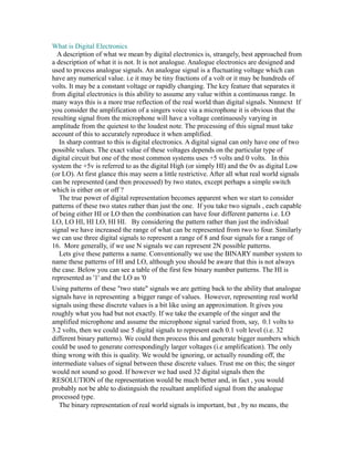
  • 1. What is Digital Electronics A description of what we mean by digital electronics is, strangely, best approached from a description of what it is not. It is not analogue. Analogue electronics are designed and used to process analogue signals. An analogue signal is a fluctuating voltage which can have any numerical value. i.e it may be tiny fractions of a volt or it may be hundreds of volts. It may be a constant voltage or rapidly changing. The key feature that separates it from digital electronics is this ability to assume any value within a continuous range. In many ways this is a more true reflection of the real world than digital signals. Nnnnext If you consider the amplification of a singers voice via a microphone it is obvious that the resulting signal from the microphone will have a voltage continuously varying in amplitude from the quietest to the loudest note. The processing of this signal must take account of this to accurately reproduce it when amplified. In sharp contrast to this is digital electronics. A digital signal can only have one of two possible values. The exact value of these voltages depends on the particular type of digital circuit but one of the most common systems uses +5 volts and 0 volts. In this system the +5v is referred to as the digital High (or simply HI) and the 0v as digital Low (or LO). At first glance this may seem a little restrictive. After all what real world signals can be represented (and then processed) by two states, except perhaps a simple switch which is either on or off ? The true power of digital representation becomes apparent when we start to consider patterns of these two states rather than just the one. If you take two signals , each capable of being either HI or LO then the combination can have four different patterns i.e. LO LO, LO HI, HI LO, HI HI. By considering the pattern rather than just the individual signal we have increased the range of what can be represented from two to four. Similarly we can use three digital signals to represent a range of 8 and four signals for a range of 16. More generally, if we use N signals we can represent 2N possible patterns. Lets give these patterns a name. Conventionally we use the BINARY number system to name these patterns of HI and LO, although you should be aware that this is not always the case. Below you can see a table of the first few binary number patterns. The HI is represented as '1' and the LO as '0 Using patterns of these "two state" signals we are getting back to the ability that analogue signals have in representing a bigger range of values. However, representing real world signals using these discrete values is a bit like using an approximation. It gives you roughly what you had but not exactly. If we take the example of the singer and the amplified microphone and assume the microphone signal varied from, say, 0.1 volts to 3.2 volts, then we could use 5 digital signals to represent each 0.1 volt level (i.e. 32 different binary patterns). We could then process this and generate bigger numbers which could be used to generate correspondingly larger voltages (i.e amplification). The only thing wrong with this is quality. We would be ignoring, or actually rounding off, the intermediate values of signal between these discrete values. Trust me on this; the singer would not sound so good. If however we had used 32 digital signals then the RESOLUTION of the representation would be much better and, in fact , you would probably not be able to distinguish the resultant amplified signal from the analogue processed type. The binary representation of real world signals is important, but , by no means, the
  • 2. only use of digital electronics. In the next section we will look at the use of these BINARY patterns to represent numbers which are manipulated as numbers without any requirement to represent an analogue signal. We will also show how these HI/LO patterns can be used to represent the logical decision making process we all take for granted Why is digital electronics important to modern technology and information processing? Digital electronics leads to fewer mistakes in sending and receiving information. Also the amount of information is greater than when using analogue electronics. Also simple tasks and basic mathematics become much easier. The principles of digital electronics The circuits and components we have discussed are very useful. You can build a radio or television with them. You can make a telephone. Even if that was all there was to electronics, it would still be very useful. However, the great breakthrough in the last fifty years or so has been in digital electronics. This is the subject which gave us the computer. The computer has revolutionised the way business, engineering and science are done. Small computers programmed to do a specific job (called microprocessors) are now used in almost every electronic machine from cars to washing machines. Computers have also changed the way we communicate. We used to have telegraph or telephone wires passing up and down a country — each one carrying one telephone call or signal. We now have optic fibres each capable of carrying tens of thousands of telephone calls using digital signals. So, what is a digital signal? Look at Figure 1. A normal signal, called an analogue signal, carries a smooth wave. At any time, the voltage of the signal could take any value. It could be 2,00 V or 3,53 V or anything else. A digital signal can only take certain voltages. The simplest case is shown in the figure — the voltage takes one of two values. It is either high, or it islow. It never has any other value. These two special voltages are given symbols. The low voltage level is written 0, while the high voltage level is written as 1. When you send a digital signal, you set the voltage you want (0 or 1), then keep this fixed for a fixed amount of time (for example 0.01 μs), then you send the next 0 or 1. The digital signal in Figure 1 could be written 01100101. Figure 1: The difference between normal (analogue) signals and digital signals. Why are digital signals so good?
  • 3. Using a computer, any information can be turned into a pattern of 0s and 1s. Pictures, recorded music, text and motion pictures can all be turned into a string of 0s and 1s and transmitted or stored in the same way. The computer receiving the signal at the other end converts it back again. A Compact Disc (CD) for example, can store music or text or pictures, and all can be read using a computer. The 0 and the 1 look very different. You can immediately tell if a 0 or a 1 is being sent. Even if there is interference, you can still tell whether the sender sent a 0 or a 1. This means that fewer mistakes are made when reading a digital signal. This is why the best music recording technologies, and the most modern cameras, for example, all use digital technology. Using the 0s and 1s you can count, and do all kinds of mathematics. This will be explained in more detail in the next section. The simplest digital circuits are called logic gates. Each logic gate makes a decision based on the information it receives. Different logic gates are set up to make the decisions in different ways. Each logic gate will be made of many microscopic transistors connected together within a thin wafer of silicon. This tiny circuit is called an Integrated Circuit or I.C. - all the parts are in one place (integrated) on the silicon wafer. .Biodiesel refers to a vegetable oil- or animal fat-based diesel fuel§ consisting of long- chain alkyl§ (methyl§, propyl§ or ethyl§) esters§. Biodiesel is typically made by chemically reacting lipids§ (e.g.,vegetable oil§, animal fat (tallow§[1][2])) with an alcohol§ producing fatty acid esters§. Biodiesel is meant to be used in standard diesel engines and is thus distinct from the vegetable and waste oils used to fuel converted diesel engines. Biodiesel can be used alone, or blended with petrodiesel. Biodiesel can also be used as a low carbon alternative to heating oil§. The National Biodiesel Board§ (USA) also has a technical definition of "biodiesel" as a mono-alkyl ester.[3] Blends of biodiesel and conventional hydrocarbon-based diesel are products most commonly distributed for use in the retail diesel fuel marketplace. Much of the world uses a system known as the "B" factor to state the amount of biodiesel in any fuel mix:[4]  100% biodiesel is referred to as B100, while  20% biodiesel, 80% petrodiesel is labeled B20  5% biodiesel, 95% petrodiesel is labeled B5  2% biodiesel, 98% petrodiesel is labeled B2.
  • 4. Blends of 20% biodiesel and lower can be used in diesel equipment with no, or only minor modifications,[5] although certain manufacturers do not extend warranty coverage if equipment is damaged by these blends. The B6 to B20 blends are covered by the ASTM§ D7467 specification.[6] Biodiesel can also be used in its pure form (B100), but may require certain engine modifications to avoid maintenance and performance problems.[7] Blending B100 with petroleum diesel may be accomplished by:  Mixing in tanks at manufacturing point prior to delivery to tanker truck  Splash mixing in the tanker truck (adding specific percentages of biodiesel and petroleum diesel)  In-line mixing, two components arrive at tanker truck simultaneously.  Metered pump mixing, petroleum diesel and biodiesel meters are set to X total volume, transfer pump pulls from two points and mix is complete on leaving pump  APPLICATION Biodiesel can be used in pure form (B100) or may be blended with petroleum diesel at any concentration in most injection pump diesel engines. New extreme high-pressure (29,000 psi) common rail§ engines have strict factory limits of B5 or B20, depending on manufacturer.[citation needed] Biodiesel has different solvent§ properties than petrodiesel, and will degrade natural rubber§ gaskets§ and hoses§ in vehicles (mostly vehicles manufactured before 1992), although these tend to wear out naturally and most likely will have already been replaced with FKM§, which is nonreactive to biodiesel. Biodiesel has been known to break down deposits of residue in the fuel lines where petrodiesel has been used.[8] As a result, fuel filters§ may become clogged with particulates if a quick transition to pure biodiesel is made. Therefore, it is recommended to change the fuel filters on engines and h AVABALITY & PRICE Global biodiesel production§ reached 3.8 million tons in 2005. Approximately 85% of biodiesel production came from the European Union.[citation needed] In 2007, in the United States, average retail (at the pump) prices, including federal and state fuel taxes§, of B2/B5 were lower than petroleum§ diesel by about 12 cents, and B20 blends were the same as petrodiesel.[42] However, as part as a dramatic shift in diesel pricing, by July 2009, the US DOE was reporting average costs of B20 15 cents per gallon higher than petroleum diesel ($2.69/gal vs. $2.54/gal).[43] B99 and B100 generally cost more than petrodiesel except where local governments provide a tax incentive or subsidy. BIODIESA; FEED BACK A variety of oils can be used to produce biodiesel. These include:  Virgin oil feedstock – rapeseed and soybean oils§ are most commonly used, soybean oil alone accounting for about ninety percent of all fuel stocks in the US. It also can be obtained from Pongamia§, field pennycress§ and jatropha§ and other crops such as mustard§, jojoba§, flax§, sunflower§, palm oil§, coconut§, hemp§ (see list of vegetable oils for biofuel§ for more information);  Waste vegetable oil§ (WVO);
  • 5.  Animal fats§ including tallow§, lard§, yellow grease§, chicken fat,[56] and the by-products of the production of Omega-3 fatty acids§ from fish oil.  Algae§, which can be grown§ using waste materials such as sewage[57] and without displacing land currently used for food production.  Oil from halophytes§ such as Salicornia bigelovii§, which can be grown using saltwater in coastal areas where conventional crops cannot be grown, with yields equal to the yields of soybeans and other oilseeds grown using freshwater irrigation[58] CURRENT RESERCH There is ongoing research into finding more suitable crops and improving oil yield. Other sources are possible including human fecal matter, with Ghana§ building its first "fecal sludge-fed biodiesel plant." [96] Using the current yields, vast amounts of land and fresh water would be needed to produce enough oil to completely replace fossil fuel usage. It would require twice the land area of the US to be devoted to soybean production, or two- thirds to be devoted to rapeseed production, to meet current US heating and transportation needs.[citation needed] Specially bred mustard varieties can produce reasonably high oil yields and are very useful in crop rotation§ with cereals, and have the added benefit that the meal leftover after the oil has been pressed out can act as an effective and biodegradable pesticide.[97] The NFESC§, with Santa Barbara§-based Biodiesel Industries is working to develop biodiesel technologies for the US navy and military, one of the largest diesel fuel users in the world.[98] A group of Spanish developers working for a company called Ecofasa§ announced a new biofuel made from trash. The fuel is created from general urban waste which is treated by bacteria to produce fatty acids, which can be used to make biodiesel.[99] Another approach that does not require the use of chemical for the production involves the use of genetically modified microbes.[100][101] Sagarika (missile) [edit§]Development Development of the K-15 missile started in the late 1990s with the goal of building a submarine-launched ballistic missile for use with the Indian Navy§ nuclear-powered Arihant class submarines§.[6][7] Sagarika has a length of 10 metres (33 ft), diameter of 0.74 metres (2 ft 5 in), weighs 17 tonnes and can carry a payload of up to 1,000 kilograms (2,205 lb) over 700 kilometres (435 mi). It was developed at the DRDO§’s missile complex in Hyderabad§.[8] The development of the underwater missile launcher, known as Project 420, was completed in 2001 and handed over to the Indian Navy§ for trials. The missile launcher is developed at Hazira in Gujarat§.[9] The Sagarika missile began integration with India's nuclear-powered§ Arihant class submarine§ that began sea trials on the 26 July 2009.[10] By 2008, the missile was successfully test fired seven times, and tested to its full range up
  • 6. to four times. The tests of February 26, 2008, were conducted from a submerged pontoon 50 metres (160 ft) beneath the surface off the coast of Visakhapatnam§.[6][8][11][12] A land-based version of the K-15 Sagarika was successfully test-fired on November 12, 2008.[13] A full range test of the missile was done on 11 March 2012.[14] The twelfth and final development trial of the missiles was conducted on 27 January 2013. According toV.K. Saraswat§, the missile was again tested for its full range of 7 Yesterday India successfully test-fired the underwater ballistic missile, Sagarika K-15 (code-named B05), off the Visakhapatnam coast, marking en end to a series of developmental trials. The trail was conducted on a day when China tested a missile defence system, an interceptor. K-15 Sagarika is a nuclear-capable submarine-launched ballistic missile with a range of 700 kilometres (435 mi). In its twelfth flight trial, the 10-metre tall Submarine-Launched Ballistic Missile (SLBM) lifted off from a pontoon, rose to an altitude of 20 km and reached a distance of about 700 km as it splashed down in the waters of the Bay of Bengal near the pre-designated target point. According to scientific advisor to the Defence Minister V.K. Saraswat, the missile was tested for its full range of 700 km and the mission met all its objectives. He said the impact accuracy of the medium range strategic missile was in single digit. With the completion of developmental trials, the process of integrating K-15 missile with INS Arihant, the indigenously-built nuclear submarine, will begin soon. As many as 12 nuclear-tipped missiles, each weighing six tonnes will be integrated with Arihant, which will be powered by an 80 MWt (thermal) reactor that uses enriched uranium as fuel and light water as coolant and moderator. India is only the fifth country to have such a missile — the other four nations being the United States, Russia, France and China. Read more: Meanwhile the reactor has been integrated with the submarine and it was expected to go critical in May/ June 2013. Once that was done, the harbour trials will begin. Read more: New Delhi: India’s 700 kms range Sagarika (K-15) submarine launched ballistic missile (SLBM) tested on 16 March 2012, was unsuccessful. This was the second test within a span of five days. The first test in the last fortnight, was carried out on 11 March which was reported to be successful. Both tests took place about 10 kms off Visakhapatam on the east coast of India. In the absence of a submarines, the missile tests were carried out from a submerged pontoon, simulating a submarine. Sagarika is a DRDO project. According to sources, the second test of 16 March was not successful due to very rough sea condition. The sea condition was so rough that some Indian Navy personnel on board a logistic support ship fell sick. The ship was positioned a few kms away from the pontoon to provide logistic support. The fire control systems was on the ship and the ship
  • 7. and the pontoon were connected by a cable for launch of the missile. “With the approaching monsoon, the sea conditions will remain disturbed, so the next test of Sagarika now can be conducted only after September this year,” sources said. Sagarika, code-named K-15 missile is a nuclear-capable submarine launched tactical missile. The missile is developed for use with India’s Arihant class nuclear submarines. First of this class submarine is now on sea trials K-15 forms part of India’s nuclear triad as deterrence against a nuclear threat from its hostile neighbours- Pakistan and China. SLBM gives India a second strike capability while following its policy of no first use of nuclear weapons. “The first test of Sagarika on 11 March was successful and the missile covered full range of 700 km and hit the designated target, but the second test of 16 March was not successful,” sources said. K-15 can carry a nuclear or conventional warheads of about 500 kg. Sagarika is an advanced version ot the Prithvi ballistic missile. The surface-launched variant of Sagarika is called Shourya. The first successful test firing of the missile took place on 26 February 2008. The missile is developed by DRDO at its complex in Hyderabad. This complex houses the Defence Research and Development Laboratory (DRDL), the Advanced Systems Laboratory(ASL) and the Research Center, Imarat (RCI). ndian state of Gujarat chief minister Narendra Modi greets his supporters after casting his vote in the second phase of state-assembly elections in Ahmedabad, India, on Dec. 17, 2012 Next p.m Gujarat’s bookies are probably lying low for the next few days. The good odds they put on a narrow win§ for Narendra Modi did not pay off today, as the charismatic and divisive Indian politician was re-elected as chief minister of the western Indian state in a decisive victory. The win — Modi’s Bharatiya Janata Party (BJP) won 115 of 182 of the state assembly’s seats — is a strong stamp of approval for the party and the Hindu nationalist politico himself, who has played a pivotal role in setting Gujarat on a path of enviable growth. It also marks a major defeat for the Congress Party, which came in at a distant second with 61 seats, and raises the stakes in the battle between India’s ruling party and the BJP for hearts and minds in the run-up to national elections scheduled for 2014. “There was a thinking in our politics that good economics is bad politics,” Modi said in his victory speech§ on Thursday. “Development won today.” Few figures in Indian politics have the kind of devoted following that Modi, 62, enjoys today. The feverishly loyal supporters who gave their chief minister another run in office this week believe he has turned the state around, creating a rare, business-friendly environment that has brought money, infrastructure and much needed jobs to this important coastal state. (Read a victory blog post§ from Modi.) At the same time, few figures have been as polarizing. Controversy has followed Modi since 2002, when, after 58 people were killed in an arson attack on two train carriages
  • 8. carrying Hindu activists, Gujarat erupted in a spasm of brutal anti-Muslim riots. As many as 2,000 Muslims were killed in the violence that followed, and 10 years later, many in India still blame Modi, who was chief minister at that time too, and his colleagues for their alleged complicity in the attacks. Modi has always firmly denied such accusations. When asked about his role in the riots in an interview with TIME earlier this year, he refused to comment on the subject. “Let people say what they want to say. My actions speak.” In October this year, the U.K. government announced that it had instructed its high commissioner in New Delhi to re-engage with the Gujarat state administration. Modi has been denied visas to the U.S. in the past, however, and 25 American lawmakers recently called on President Barack Obama to do so should Modi seek entry to the U.S. again. That poses a potentially awkward scenario as Modi inches closer to seeking the country’s top job. His election team ran what was surely one of the most ambitious state campaigns that India has seen, employing 3-D holographic technology§ so he could deliver stump speeches in dozens of locations at once. (The tactic, intended to highlight the state’s technological prowess, drew immediate criticism from Congress, which demanded the Election Commission look into how the gimmick was funded.) The stakes here are high: without this win, Modi risked losing the momentum he will need if he wants — as many think he does — to try to bring his political career to the national stage in 2014. Modi has never publicly said he wants to be the next Prime Minister of India. But senior BJP leaders have floated his name many times, setting the stage for a possible showdown between Modi and Rahul Gandhi during campaigning next December. Though he was not running for any seat in Gujarat, as Congress’ general secretary, Gandhi has become central to his party’s 2014 election campaign. It is still unclear whether the 42-year-old will take over the reins if a Congress-led government were to be voted into office in 2014. Like Modi, he has never stated that he covets the spot at the top of India’s political scrum. But unlike Modi, many in India speculate that Gandhi doesn’t actually want the job. Doubts about his appetite for the post were recently raised again when, in a recent Cabinet reshuffle, he did not take a ministerial position. Nevertheless, as India’s two main political parties fought over Gujarat this month, Gandhi led the charge. The politicians exchanged several pointed barbs in the days before the polls. Before a packed rally earlier this month, Gandhi said to a crowd of Congress supporters: “I was told that Gujarat has been shining, all due to the efforts of one man … Do you have electricity? Do you have water? Do the youths here have jobs?” The crowd cried back: “No!” Derailing Team Modi’s narrative that Gujarat is excelling in development and economic growth had been one of Congress’ key strategies in fighting his re-election. Modi’s highly effective p.r. crew has been peddling the story of Gujarat’s growth for many months, touting its development policies as a model for other Indian states. Their claims are not baseless. As noted in this magazine’s March cover story§ on Modi: Today, Gujarat is the only state in India where both big businesses and small farmers can expect an uninterrupted power supply for nearly 24 hours a day, with the premium rates paid by big business used to subsidize rural electrification. In 10 years, Gujarat’s auto
  • 9. industry has grown from one modest plant to an expected capacity of 700,000 cars in 2014, including billion-dollar investments announced last year by Ford and Peugeot. Those are positive numbers, the likes of which only a few other Indian states can match. But as elections got under way, some questioned§ whether Gujarat’s growth has translated into the levels of poverty reduction that it should have, drawing attention§ to the widening rich-poor divide in some parts of the state. For others, the specter of such a polarizing figure leading the nation raises questions much larger than whether trickle- down economics is working in western India. Modi’s critics fret over how a man associated with one of the worst cases of communal violence in India is the right person to move this diverse country forward. It’s a question that BJP leaders are no doubt thinking hard about as they ruminate who will be the next front man for their party. But millions of Gujaratis have already made up their mind. As one supporter tweeted out on Thursday: “Modi is my PM because he’s growth-focused, decisive, tactful, visionary and good at marketing.” Whether or not it was a typo — Modi was just re-elected CM of Gujarat, not PM of India — is unclear, but it’s probably not an error that anyone on his celebrating team would try to correct anytime soon. TRANSISROR The essential usefulness of a transistor comes from its ability to use a small signal applied between one pair of its terminals to control a much larger signal at another pair of terminals. This property is called gain§. A transistor can control its output in proportion to the input signal; that is, it can act as an amplifier§. Alternatively, the transistor can be used to turn current on or off in a circuit as an electrically controlled switch§, where the amount of current is determined by other circuit elements. There are two types of transistors, which have slight differences in how they are used in a circuit. A bipolar transistor§ has terminals labeled base, collector, and emitter. A small current at the base terminal (that is, flowing between the base and the emitter) can control or switch a much larger current between the collector and emitter terminals. For a field- effect transistor§, the terminals are labeled gate, source, and drain, and a voltage at the gate can control a current between source and drain. The image to the right represents a typical bipolar transistor in a circuit. Charge will flow between emitter and collector terminals depending on the current in the base. Since internally the base and emitter connections behave like a semiconductor diode, a voltage drop develops between base and emitter while the base current exists. The amount of this voltage depends on the material the transistor is made from, and is referred to as VBE. Transistor as a switch § § BJT used as an electronic switch, in grounded-emitter configuration.
  • 10. Transistors are commonly used as electronic switches, both for high-power applications such as switched-mode power supplies§ and for low-power applications such as logic gates§. In a grounded-emitter transistor circuit, such as the light-switch circuit shown, as the base voltage rises, the emitter and collector currents rise exponentially. The collector voltage drops because of the collector load resistance (in this example, the resistance of the light bulb). If the collector voltage were zero, the collector current would be limited only by the light bulb resistance and the supply voltage. The transistor is then said to be saturated - it will have a very small voltage from collector to emitter. Providing sufficient base drive current is a key problem in the use of bipolar transistors as switches. The transistor provides current gain, allowing a relatively large current in the collector to be switched by a much smaller current into the base terminal. The ratio of these currents varies depending on the type of transistor, and even for a particular type, varies depending on the collector current. In the example light-switch circuit shown, the resistor is chosen to provide enough base current to ensure the transistor will be saturated. In any switching circuit, values of input voltage would be chosen such that the output is either completely off,[21] or completely on. The transistor is acting as a switch, and this type of operation is common in digital circuits§ where only "on" and "off" values are relevant. Transistor as an amplifier § § Amplifier circuit, common- emitter configuration with a voltage-divider bias circuit. The common-emitter amplifier§ is designed so that a small change in voltage (Vin) changes the small current through the base of the transistor; the transistor's current amplification combined with the properties of the circuit mean that small swings in Vin produce large changes in Vout. Various configurations of single transistor amplifier are possible, with some providing current gain, some voltage gain, and some both. From mobile phones§ to televisions§, vast numbers of products include amplifiers for sound reproduction§, radio transmission§, and signal processing§. The first discrete transistor audio amplifiers barely supplied a few hundred milliwatts, but power and audio fidelity gradually increased as better transistors became available and amplifier architecture evolved. Modern transistor audio amplifiers of up to a few hundred watts§ are common and relativel
  • 11. WHAT IS BISISNG ans : "Biasing" applies to transistor amplifier circuits. Simple amplifier circuits can only amplify positive signals. Negative signals cause the amplifier to shut down. However, AC signals in general have both a positive and a negative part. To allow a transistor to amplify AC, we add a positive voltage to the AC signal. Then after it is amplified, we remove the positive voltage again. The voltage, ac or dc on the base, compared to the emitter to cause operation of the transistor to conduct to the collector or to the emiiter in a NPN transistor. TYES OF BISING A transistor is a semiconductor used for amplification or switching electrical signals. A transistor contains three terminals to connect with an external circuit. Biasing is the bias point on the output of the DC emitter voltage and the flow of current controlled by a transistor. Biasing networks are used when circuits are made with discrete circuit devices. There are various types of transistor biasing, detailed here. Bipolar Transistor Biasing A type of bipolar transistor biasing is an amplifier. Bipolar transistor amplifiers must be biased in order to operate. With Class A amplifiers, you can use different types of bias circuits, such as fixed bias, emitter bias and collector-stabilized biasing circuit. Bipolar Junction Transistor Biasing In bipolar junction transistor, the bias point enables the transistor to operate in active mode. The bias point stabilizes the current and the Q-point DC voltage. The bias point determines the operating point (biasing); you must not shift the transistor to any position. RF Power Transistors Biasing A power transistor includes two components on one semiconductor die. You must bias the two transistor components. A network couples the transistor component terminals in the middle of a ground and a bias voltage. One transistor component is biased first, Class A operation. Another transistor component is biased second, Class B operation. Field Effect Transistor Biasing You must bias a field-effect transistor with two voltages. One electrode must be polarized from a voltage biased through a transistor. The transistor must be in saturable load operation. The saturable load's gate and main transistor's gate are connected and supported by two bias voltages. The saturable load's gate voltage follows the main transistor's voltage. Lateral Power Transistor Biasing A lateral power transistor contains one drift region and a well region. Both regions contain high amounts of silicon. Place the second silicon region laterally from the well region. When biasing the transistor, a current flows through the drift region in a lateral
  • 12. position in between the two silicon regions. Need of bising A BJT (Bipolar Junction Transistor) require a voltage normally in the range of 0.7V for the internal junctions to become conductive. It is a fixed parameter of Silicon (Si) due to the amount of 1.1eV required to get electrons from the valence energy band into a conductive band. To be able jump the energy gap which is a forbidden band for electrons or to raise the Fermi energy level in the atom. The energy, whether it is electrically applied, thermally or optically, is required to be able change the state of a semiconductor from an insulator to an conductor. You can read more on "semiconductor theory" for better understanding. Then with a non-linear relationship the conductivity will increase as one increase the forward bias current through the base to emitter junction. Biasing is used for classical transistor amplifier applications. Biasing is required to have the transistor half way saturated for Class-A amplification or barely switched on for Class-B power amplifiers. If a Class-B amplifier is not biased, then the lower 0.7V of the audio or sine wave will not be amplified causing crossover distortion. When you bias it correctly, the distortions will be gone, since the entire half wave will then fit into the on state of the transistor. If a Class-A amplifier is not correctly biased, premature clipping on the positive or negative part of the wave will occur. Biasing may be used for other applications as well, such as photo transistors, internal construction of IC's such as op-amp Bipolar junction transistors For bipolar junction transistors§ the bias point is chosen to keep the transistor operating in the active mode, using a variety of circuit techniques§, establishing the Q-point DC voltage and current. A small signal is then applied on top of the Q-point bias voltage, thereby either modulating§ or switching the current, depending on the purpose of the circuit. The quiescent point of operation is typically near the middle of the DC load line§. The process of obtaining a certain DC collector current at a certain DC collector voltage by setting up the operating point is called biasing. After establishing the operating point, when an input signal is applied, the output signal should not move the transistor either to saturation or to cut-off. However, this unwanted shift still might occur, due to the following reasons: 1 Parameters of transistors depend on junction temperature. As junction temperature increases, leakage current due to minority charge carriers (ICBO) increases. As ICBO increases, ICEO also increases, causing an increase in collector current IC. This produces heat at the collector junction. This process repeats, and, finally, the Q-point may shift into the saturation region. Sometimes, the excess heat produced at the junction may even burn the transistor. This is known as thermal runaway§. 2 When a transistor is replaced by another of the same type, the Q-point may shift, due to changes in parameters of the transistor, such as current gain () which varies slightly for each unique transistor.
  • 13. To avoid a shift of Q-point, bias-stabilization is necessary. Various biasing circuits§ can be used for this purpose. Q. 9. What are bias compensation methods? Explain diode compensation for self bias circuit. Ans. Compensation techniques refer to the use of temperature sensitive devices such as diodes, transistors, thermistors etc. which provide compensating voltages and currents to maintain the operating point constant. In comparison, stabilization technique use only resistive biasing circuits. Due to bias circuit, feedback is there and it reduce drastically the amplification of the signal. If this loss in signal gain is intolerable in particular application, it is often possible to use compensating techniques to reduce the drift of the operating point. Diode compensation for : A circuit utilizing self bias stabilizing technique and diode compensation is shown. The diode is kept biased in the forward direction by the source and resistance . If the diode is of same material and type of transistor, the voltage across the diode will have the same temperature coefficient as the base to emitter voltage . If KVL is applied around the base circuit then, Since tracks w.r.t. temperature, then will be insensitive to variations in . In practice, the compensation of is not like this exact, but it is sufficiently effective to take care of great part of transistor drift due to variations in Diode Compensation for : The changes of with temperature contribute significantly to changes in collector current of Si transistors. On the other hand, for Ge transistors changes in with temperature play the more important role in collector current stability. The compensation circuit is shown. It offers stabilization against variations of If diode and the transistor are of same type and material, The reverse saturation current of the diode will increase with temperature at the same rate as the transistor collector saturation current . Now Since the diode is reverse biased by an amount for Ge devices, it follows that the current through D is . The base current . A load line is used in graphical analysis of nonlinear§ electronic circuits§, representing the constraint other parts of the circuit place on a non-linear§ device, like a diode§ or transistor§. It is usually drawn on a graph of the current§ vs the voltage§ in the nonlinear device, called the device's characteristic curve§. A load line, usually a straight line, represents the response of a linear circuit§ connected to the nonlinear device in question. The operating point(s) of the circuit are the points where the characteristic curve and the
  • 14. load line intersect; at these points the current and voltage parameters of both parts of the circuit match.[1] The example at right shows how a load line is used to determine the current and voltage in a simple diode§ circuit. The nonlinear diode is in series with a linear circuit consisting of a resistor§ and a voltage§ source. The graph, representing voltage across the diode VD versus current I through the diode, is an exponential curve. The load line (diagonal line)represents the relationship between current and voltage in the linear part of the circuit. Since the current going through the three elements in series must be the same, and the voltage at the connection of the resistor and diode must be the same, the operating point of the circuit will be at the intersection of the curve with the load line. In a BJT§ circuit, the BJT has a different current-voltage (IC-VCE) characteristic depending on the base current. Placing a series of these curves on the graph shows how the base current will affect the operating point of the circuit. DC and AC load lines Semiconductor§ circuits typically have both DC§ and AC§ currents in them, with a source of DC current to bias§ the nonlinear semiconductor to the correct operating point, and the AC signal superimposed on the DC. Load lines can be used separately for both DC and AC analysis. The DC load line is the load line of the DC equivalent circuit§, defined by reducing the reactive components to zero (replacing capacitors by open circuits and inductors by closed circuits). It is used to determine the correct DC operating point, often called the Q point§. Once a DC operating point is defined by the DC load line, an AC load line with, in general, a different slope can be drawn, through the DC operating point, to calculate the AC output. Because the impedance of the reactive components will vary with frequency, the slope of the AC load line depends on the frequency of the applied signal. So there are many AC load lines, that vary from the DC load line (at low frequency) to a limiting AC load line, all having a common intersection at the dc operating point. This limiting load line, generally referred to as the AC load line, is the load line of the circuit at "infinite frequency", and can be found be replacing capacitors with short circuits, and inductors with open circuits. [edit§]Load lines for common configurations [edit§]Transi stor load line § Common emitter transistor load line. The load line diagram at right is for a
  • 15. transistor connected in a common emitter§ circuit. It shows the collector current in the transistor IC versus collector voltageVCE for different values of base current Ibase. The load line represents a particular value of collector load resistor (RC). The intersections of the load line with the transistor characteristic curve represent the different values of IC and VCE at different base currents. The point on the load line where it intersects the collector current axis is referred to as saturation point.[2] At this point, the transistor current is maximum and voltage across collector is minimum, for a given load. For this circuit, IC-SAT= VCC/RC.[3] The cutoff point is the point where the load line intersects with the collector voltage axis. Here the transistor current is minimum (approximately zero) and emitter is grounded. Hence VCE-CUTOFF=Vcc. The operating point of the circuit in this configuration is generally designed to be in the active region, approximately between middle of the load line and close to saturation point. In this region, the collector current is proportional to the base current, and hence useful for amplifier§ applications. a load line is normally drawn on ic-vce characteristics curves for the transistor used in amplifier circuit.
  • 16. transistor connected in a common emitter§ circuit. It shows the collector current in the transistor IC versus collector voltageVCE for different values of base current Ibase. The load line represents a particular value of collector load resistor (RC). The intersections of the load line with the transistor characteristic curve represent the different values of IC and VCE at different base currents. The point on the load line where it intersects the collector current axis is referred to as saturation point.[2] At this point, the transistor current is maximum and voltage across collector is minimum, for a given load. For this circuit, IC-SAT= VCC/RC.[3] The cutoff point is the point where the load line intersects with the collector voltage axis. Here the transistor current is minimum (approximately zero) and emitter is grounded. Hence VCE-CUTOFF=Vcc. The operating point of the circuit in this configuration is generally designed to be in the active region, approximately between middle of the load line and close to saturation point. In this region, the collector current is proportional to the base current, and hence useful for amplifier§ applications. a load line is normally drawn on ic-vce characteristics curves for the transistor used in amplifier circuit.