
Empfohlen
Weitere ähnliche Inhalte
Was ist angesagt?
Was ist angesagt? (20)
Ähnlich wie Amplitude modulation
Ähnlich wie Amplitude modulation (20)
Mehr von Rumah Belajar
Mehr von Rumah Belajar (20)
Kürzlich hochgeladen
Kürzlich hochgeladen (20)
Amplitude modulation
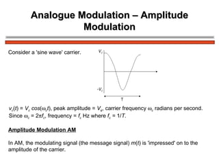
- 1. Analogue Modulation – Amplitude Modulation v c ( t ) = V c cos ( c t ), peak amplitude = V c , carrier frequency c radians per second. Since c = 2 f c , frequency = f c Hz where f c = 1/ T . Consider a 'sine wave' carrier. Amplitude Modulation AM In AM, the modulating signal (the message signal) m ( t ) is 'impressed' on to the amplitude of the carrier.
- 2. Message Signal m ( t ) In general m ( t ) will be a band of signals, for example speech or video signals. A notation or convention to show baseband signals for m ( t ) is shown below
- 3. Message Signal m ( t ) In general m ( t ) will be band limited. Consider for example, speech via a microphone. The envelope of the spectrum would be like:
- 4. Contoh
- 5. Contoh
- 6. Message Signal m ( t ) In order to make the analysis and indeed the testing of AM systems easier, it is common to make m ( t ) a test signal, i.e. a signal with a constant amplitude and frequency given by
- 7. Schematic Diagram for Amplitude Modulation V DC is a variable voltage, which can be set between 0 Volts and + V Volts. This schematic diagram is very useful; from this all the important properties of AM and various forms of AM may be derived.
- 8. Equations for AM From the diagram where V DC is the DC voltage that can be varied. The equation is in the form Amp cos c t and we may 'see' that the amplitude is a function of m ( t ) and V DC . Expanding the equation we get:
- 9. Equations for AM Now let m ( t ) = V m cos m t, i.e. a 'test' signal, Using the trig identity we have Components: Carrier upper sideband USB lower sideband LSB Amplitude: V DC V m /2 V m /2 Frequency: c c + m c – m f c f c + f m f c + f m This equation represents Double Amplitude Modulation – DSBAM
- 10. Spectrum and Waveforms The following diagrams represent the spectrum of the input signals, namely ( V DC + m ( t )), with m ( t ) = V m cos m t , and the carrier cos c t and corresponding waveforms.
- 11. Spectrum and Waveforms The above are input signals. The diagram below shows the spectrum and corresponding waveform of the output signal, given by
- 12. Spektrum 2 sisi
- 13. Double Sideband AM, DSBAM The component at the output at the carrier frequency f c is shown as a broken line with amplitude V DC to show that the amplitude depends on V DC . The structure of the waveform will now be considered in a little more detail. Waveforms Consider again the diagram V DC is a variable DC offset added to the message; m ( t ) = V m cos m t
- 14. Double Sideband AM, DSBAM This is multiplied by a carrier, cos c t . We effectively multiply ( V DC + m ( t )) waveform by +1, -1, +1, -1, ... The product gives the output signal
- 15. Double Sideband AM, DSBAM
- 16. Modulation Depth Consider again the equation , which may be written as The ratio is defined as the modulation depth , m , i.e. Modulation Depth From an oscilloscope display the modulation depth for Double Sideband AM may be determined as follows:
- 17. Modulation Depth 2 2 E max = maximum peak-to-peak of waveform 2 E min = minimum peak-to-peak of waveform Modulation Depth This may be shown to equal as follows: = =
- 19. Graphical Representation of Modulation Depth and Modulation Types.
- 20. Graphical Representation of Modulation Depth and Modulation Types 2.
- 21. Graphical Representation of Modulation Depth and Modulation Types 3 Note then that V DC may be set to give the modulation depth and modulation type. DSBAM V DC >> V m , m 1 DSB Dim C 0 < V DC < V m , m > 1 (1 < m < ) DSBSC V DC = 0, m = The spectrum for the 3 main types of amplitude modulation are summarised
- 22. Bandwidth Requirement for DSBAM In general, the message signal m ( t ) will not be a single 'sine' wave, but a band of frequencies extending up to B Hz as shown Remember – the 'shape' is used for convenience to distinguish low frequencies from high frequencies in the baseband signal.
- 24. Power Considerations in DSBAM Remembering that Normalised Average Power = ( V RMS ) 2 = we may tabulate for AM components as follows: Total Power P T = Carrier Power P c + P USB + P LSB Power Power V DC Amplitude pk LSB USB Carrier Component
- 25. Power Considerations in DSBAM From this we may write two equivalent equations for the total power P T , in a DSBAM signal The carrier power and or i.e. Either of these forms may be useful. Since both USB and LSB contain the same information a useful ratio which shows the proportion of 'useful' power to total power is
- 26. Power Considerations in DSBAM For DSBAM ( m 1), allowing for m ( t ) with a dynamic range, the average value of m may be assumed to be m = 0.3 Hence, on average only about 2.15% of the total power transmitted may be regarded as 'useful' power. ( 95.7% of the total power is in the carrier!) Hence, Even for a maximum modulation depth of m = 1 for DSBAM the ratio i.e. only 1/6th of the total power is 'useful' power (with 2/3 of the total power in the carrier).
- 27. Grafik
- 28. Example Suppose you have a portable (for example you carry it in your ' back pack') DSBAM transmitter which needs to transmit an average power of 10 Watts in each sideband when modulation depth m = 0.3. Assume that the transmitter is powered by a 12 Volt battery. The total power will be where = 10 Watts, i.e. = 444.44 Watts Hence, total power P T = 444.44 + 10 + 10 = 464.44 Watts. Hence, battery current (assuming ideal transmitter) = Power / Volts = i.e. a large and heavy 12 Volt battery. amps! Suppose we could remove one sideband and the carrier, power transmitted would be 10 Watts, i.e. 0.833 amps from a 12 Volt battery, which is more reasonable for a portable radio transmitter.
- 29. Single Sideband Amplitude Modulation One method to produce signal sideband (SSB) amplitude modulation is to produce DSBAM, and pass the DSBAM signal through a band pass filter, usually called a single sideband filter, which passes one of the sidebands as illustrated in the diagram below. The type of SSB may be SSBAM (with a 'large' carrier component), SSBDimC or SSBSC depending on V DC at the input. A sequence of spectral diagrams are shown on the next page.
- 30. Single Sideband Amplitude Modulation
- 31. Single Sideband Amplitude Modulation Note that the bandwidth of the SSB signal B Hz is half of the DSB signal bandwidth. Note also that an ideal SSB filter response is shown. In practice the filter will not be ideal as illustrated. As shown, with practical filters some part of the rejected sideband (the LSB in this case) will be present in the SSB signal. A method which eases the problem is to produce SSBSC from DSBSC and then add the carrier to the SSB signal.
- 32. Single Sideband Amplitude Modulation
- 33. Single Sideband Amplitude Modulation with m ( t ) = V m cos m t , we may write: The SSB filter removes the LSB (say) and the output is Again, note that the output may be SSBAM, V DC large SSBDimC, V DC small SSBSC, V DC = 0 For SSBSC, output signal =
- 34. Power in SSB From previous discussion, the total power in the DSB signal is Hence, if P c and m are known, the carrier power and power in one sideband may be determined. Alternatively, since SSB signal = then the power in SSB signal (Normalised Average Power) is Power in SSB signal = = for DSBAM.
- 36. Envelope or Non-Coherent Detection This is obviously simple, low cost. But the AM input must be DSBAM with m << 1, i.e. it does not demodulate DSBDimC, DSBSC or SSBxx. An envelope detector for AM is shown below:
- 37. Large Signal Operation For large signal inputs, ( Volts) the diode is switched i.e. forward biased ON, reverse biased OFF, and acts as a half wave rectifier. The 'RC' combination acts as a 'smoothing circuit' and the output is m ( t ) plus 'distortion'. If the modulation depth is > 1, the distortion below occurs
- 38. Small Signal Operation – Square Law Detector For small AM signals (~ millivolts) demodulation depends on the diode square law characteristic. The diode characteristic is of the form i ( t ) = av + bv2 + cv3 + ... , where i.e. DSBAM signal.
- 39. Small Signal Operation – Square Law Detector = = = 'LPF' removes components. Signal out = i.e. the output contains m ( t ) i.e.
- 40. Synchronous or Coherent Demodulation A synchronous demodulator is shown below This is relatively more complex and more expensive. The Local Oscillator (LO) must be synchronised or coherent, i.e. at the same frequency and in phase with the carrier in the AM input signal. This additional requirement adds to the complexity and the cost. However, the AM input may be any form of AM, i.e. DSBAM, DSBDimC, DSBSC or SSBAM, SSBDimC, SSBSC. (Note – this is a 'universal' AM demodulator and the process is similar to correlation – the LPF is similar to an integrator).
- 41. Synchronous or Coherent Demodulation If the AM input contains a small or large component at the carrier frequency, the LO may be derived from the AM input as shown below.
- 42. Synchronous (Coherent) Local Oscillator If we assume zero path delay between the modulator and demodulator, then the ideal LO signal is cos( c t ). Note – in general the will be a path delay, say , and the LO would then be cos( c ( t – ), i.e. the LO is synchronous with the carrier implicit in the received signal. Hence for an ideal system with zero path delay Analysing this for a DSBAM input =
- 43. Synchronous (Coherent) Local Oscillator V X = AM input x LO = We will now examine the signal spectra from 'modulator to V x' = =
- 44. Synchronous (Coherent) Local Oscillator (continued on next page)
- 45. Synchronous (Coherent) Local Oscillator Note – the AM input has been 'split into two' – 'half' has moved or shifted up to and half shifted down to baseband, and and and and and and
- 47. 1. Double Sideband (DSB) AM Inputs The equation for DSB is diminished carrier or suppressed carrier to be set. where VDC allows full carrier (DSBAM), Hence, Vx = AM Input x LO Since
- 48. 1. Double Sideband (DSB) AM Inputs The LPF with a cut-off frequency f c Hz will remove the components at 2 c (i.e. components above c ) and hence Obviously, if and we have, as previously Consider now if is equivalent to a few Hz offset from the ideal LO. We may then say The output, if speech and processed by the human brain may be intelligible, but would include a low frequency 'buzz' at , and the message amplitude would fluctuate. The requirement = 0 is necessary for DSBAM.
- 49. 1. Double Sideband (DSB) AM Inputs Consider now if is equivalent to a few Hz offset from the ideal LO. We may then say The output, if speech and processed by the human brain may be intelligible, but would include a low frequency 'buzz' at , and the message amplitude would fluctuate. The requirement = 0 is necessary for DSBAM. Consider now that = 0 but 0, i.e. the frequency is correct at c but there is a phase offset. Now we have 'cos( )' causes fading (i.e. amplitude reduction) of the output.
- 51. 1. Double Sideband (DSB) AM Inputs If the phase offset varies with time, then the signal fades in and out. The variation of amplitude of the output, with phase offset is illustrated below Thus the requirement for = 0 and = 0 is a 'strong' requirement for DSB amplitude modulation.
- 52. 2. Single Sideband (SSB) AM Input The equation for SSB with a carrier depending on V DC is i.e. assuming Hence =
- 53. 2. Single Sideband (SSB) AM Input The LPF removes the 2 c components and hence Note, if = 0 and = 0, ,i.e. has been recovered. Consider first that 0, e.g. an offset of say 50Hz. Then If m(t) is a signal at say 1kHz, the output contains a signal a 50Hz, depending on V DC and the 1kHz signal is shifted to 1000Hz - 50Hz = 950Hz.
- 54. 2. Single Sideband (SSB) AM Input The spectrum for V out with offset is shown Hence, the effect of the offset is to shift the baseband output, up or down, by . For speech, this shift is not serious (for example if we receive a 'whistle' at 1kHz and the offset is 50Hz, you hear the whistle at 950Hz ( = +ve) which is not very noticeable. Hence, small frequency offsets in SSB for speech may be tolerated. Consider now that = 0, = 0, then
- 57. Phase Shift Method for SSB Generation The diagram below shows the Phase Shift Method for generating SSBSC f m and f c denote phase shifts at the message frequency (f m ) and the carrier frequency (f c ).
- 58. Phase Shift Method for SSB Generation Solving for V out in general terms i.e. Since The actual form of the modulation at the output will depend on the phase shifts f m and f c .
- 59. Phase Shift Method for SSB Generation Consider V out when (i.e.90 0 ) Since then When fm = 90 0 and fc = 90 0 the output is Single Sideband Suppressed Carrier – Lower Sideband. , i.e. SSBSC/LSB.
- 60. Phase Shift Method for SSB Generation Consider V out when , and since then i.e. SSBSC/USB. When f m = 90 0 and f c = -90 0 the output is Single Sideband Suppressed Carrier – Upper Sideband. Note – for m(t) as a band of signals, the phase shift f m must be the same e.g. /2 or 90 0 at all frequencies.
- 61. Exercise 1) When f m = 0 and f c = 0 show that 2) When f m = 0 and f c = show that V out = 0
- 62. Quadrature Modulation A variation on the Phase Shift Method is shown below In this form of the method, 2 different message signals m 1 (t) and m 2 (t) are input.
- 63. Quadrature Modulation The carrier is phase shifted by 90 0 to give The two carriers, and are in phase quadrature (orthogonal). Quadrature Modulation or Quadrature Multiplexing and as Independent Sideband ISB. The process is described as Clearly, .
- 64. Quadrature Modulation Each 'term' in the output is a DSBSC signal occupying the same bandwidth, but phase shifted by 90 0 relative to each other
- 65. Quadrature Modulation Demodulation will require synchronous demodulators as shown below.
- 66. Quadrature Modulation Clearly Since Since the LPF with cut-off frequency = f c , the output Similarly, Since Again, LPF removes the '2wc components, i.e.
- 67. Quadrature Modulation This type of modulation/multiplexing is used in radio systems, television and as a form of stereo multiplexing for AM radio.
- 68. Vestigial Sideband Modulation Some signals, such as TV signals contain low frequencies, or even extend down to DC. When DSB modulated we have
- 69. Vestigial Sideband Modulation It is now impossible to produce SSB, because the SSB filter would need to be ideal, as shown above. In practice the filter is as below The signal produced is called vestigial sideband, it contains the USB and a 'vestige' of the lower sideband. The BPF design is therefore less stringent. When demodulated the baseband signal is the sum of the USB and the vestige of the LSB
- 70. Vestigial Sideband Modulation Hence the original baseband signal. VSB is used in TV systems.