SlideShare ist ein Scribd-Unternehmen logo
1 von 285
Downloaden Sie, um offline zu lesen
RMKCET/DEEE/Lecture Notes/MPMC
Unit – I 8085 and 8086 PROCESSOR
Introduction to microprocessor
A microprocessor is a clock-driven semiconductor device consisting
of electronic logic circuits manufactured by using either a large-scale
integration (LSI) or very-large-scale integration (VLSI) technique.
The microprocessor is capable of performing various computing
functions and making decisions to change the sequence of program
execution.
In large computers, a CPU performs these computing functions. The
Microprocessor resembles a CPU exactly.
The microprocessor is in many ways similar to the CPU, but includes
all the logic circuitry including the control unit, on one chip.
The microprocessor can be divided into three segments for the sake of
clarity. – They are: arithmetic/logic unit (ALU), register array, and
control unit.
A comparison between a microprocessor, and a computer is shown
below:
Arithmetic/Logic Unit: This is the area of the microprocessor where
various computing functions are performed on data. The ALU unit performs
such arithmetic operations as addition and subtraction, and such logic
operations as AND, OR, and exclusive OR.
Register Array: This area of the microprocessor consists of various
registers identified by letters such as B, C, D, E, H, and L. These registers
are primarily used to store data temporarily during the execution of a
program and are accessible to the user through instructions.
Control Unit: The control unit provides the necessary timing and control
signals to all the operations in the microcomputer. It controls the flow of data
between the microprocessor and memory and peripherals.
Memory: Memory stores such binary information as instructions and data,
and provides that information to the microprocessor whenever necessary. To
execute programs, the microprocessor reads instructions and data from
memory and performs the computing operations in its ALU section. Results
are either transferred to the output section for display or stored in memory
for later use. Read-Only memory (ROM) and Read/Write memory (R/WM),
popularly known as Random- Access memory (RAM).
I/O (Input/Output): It communicates with the outside world. I/O includes
two types of devices: input and output; these I/O devices are also known as
peripherals.
System Bus: The system bus is a communication path between the
microprocessor and peripherals: it is nothing but a group of wires to carry
bits.
RMKCET/DEEE/Lecture Notes/MPMC
8085 Microprocessor
The salient features of 8085 µp are:
It is a 8 bit microprocessor.
It is manufactured with N-MOS technology.
It has 16-bit address bus and hence can address up to 216
= 65536 bytes
(64KB) memory locations through A -A .
0 15
The first 8 lines of address bus and 8 lines of data bus are multiplexed
AD – AD .
0 7
Data bus is a group of 8 lines D
0
– D .
7
It supports external interrupt request.
A 16 bit program counter (PC)
A 16 bit stack pointer (SP)
Six 8-bit general purpose register arranged in pairs: BC, DE, HL.
It requires a signal +5V power supply and operates at 3.2 MHZ single
phase clock.
It is enclosed with 40 pins DIP (Dual in line package).
Overview of 8085 microprocessor
Architecture of INTEL 8085
Intel 8085A is one of the most popular 8-bit microprocessors capable
of addressing 64KB of memory and its architecture is simple. The
architecture of 8085 includes the ALU, timing and control unit, instruction
register and decoder, register array, interrupt control and serial I/O control in
a package of 40 pins, requires +5V single power supply and can operate with
a 3MHz single phase clock.
Figure 1.1 internal architecture of 8085
Arithmetic and logic unit (ALU):
The 8085A has a simple 8 bit ALU and it works in coordination with
the accumulator, temporary register, five flags, and arithmetic and logic
circuits. ALU has the capability of performing several mathematical and
logical operations. The temporary register is used to hold the data during an
arithmetic/logic operation.
Accumulator
The accumulator is an 8-bit register that is a part of
arithmetic/logic unit (ALU). This register is used to store 8-bit data and to
RMKCET/DEEE/Lecture Notes/MPMC
perform arithmetic and logical operations. The result of an operation is stored
in the accumulator. The accumulator is also identified as register A.
Flag register
There are five flags in 8085, they are sign flag (S), zero flag (Z) ,
auxiliary carry flag (AC) , Parity flag (P) and carry flag (CY) the bit
position reserved for these flags in the flag register are shown below
S – Sign Flag: After the execution of an arithmetic/logic operation, if bit D7
of the result (usually in the accumulator) is 1, the sign flag is set. This flag is
used with signed numbers. In a given byte, if D7 is 1,the number will be
viewed as a negative number; if it is 0,the number will be considered positive.
Z – Zero Flag: The Zero flag is set if the ALU operation results is 0,and the
flag is reset if the result is not 0.This flag is modified by the result in the
accumulator as well as in the other registers.
AC – Auxiliary Carry Flag: In an arithmetic operation, when a carry is
generated by digit D3 and passed on to digit D4, the AC flag is set. The Flag is
used only internally for the programmer to change the sequence of a program
with a jump instruction.
P – Parity Flag: After an arithmetic/logic operation, if the result has an even
number of 1’s, the flag is set. If it has an odd number of 1’s flag is reset.
CY - Carry Flag: If an arithmetic operation results in a carry. The carry flag
is set; otherwise it is reset. The carry flag also serves as a borrow flag for
subtraction.
TIMING AND CONTROL UNIT:
This unit synchronizes all the microprocessor operations with the
clock and generates the control signals necessary for communication between
the microprocessor and peripherals. The control signals and indicate
the availability of data on the data bus.
INSTRUCTION REGISTER AND DECODER:
The Instruction register and decoder are part of the ALU. When an
instruction is fetched from memory, it is loaded in the instruction register.
The decoder decodes the instruction and establishes the sequence of events to
follow.
REGISTER ARRAY:
The 8085 have six general purpose registers to store eight bit data
during program execution. These registers are identified as B, C, D, E, H, and
L. They can be combined as register pairs BC, DE, and HL to perform 16 bit
operation. The programmer can use these registers to store or copy data into
the registers by using data copy instructions.
In addition to 6 general purpose register , it has two 16 bit register called
stack pointer and program counter
Program Counter (PC)
This 16-bit register deals with sequencing the execution of
instructions. This register is a memory pointer. Memory locations have 16-bit
addresses, and that is why this is a 16-bit register. The microprocessor uses
this register to sequence the execution of the instructions. The function of the
RMKCET/DEEE/Lecture Notes/MPMC
program counter is to point to the memory address from which the next byte
is to be fetched. When a byte (machine code) is being fetched, the program
counter is incremented by one to point to the next memory location
Stack Pointer (SP)
The stack pointer is also a 16-bit register used as a memory pointer. It points
to a memory location in R/W memory, called the stack. The beginning of the
stack is defined by loading 16-bit address in the stack pointer.
COMMUNICATION LINES:
8085 MPU performs data transfer operation using three sets of
communication lines called buses: the address bus, the data bus, and the
control bus.
ADDRESS BUS:
The address bus is a group of 16 lines generally identified as A0 to
A15.The address bus is unidirectional i.e. bits flow in one direction from MPU
to peripheral devices. The 8085 MPU with its 16 address lines is capable of
addressing 216
= 65,536(64K) bytes memory location.
DATA BUS:
The data bus is a group of 8 lines used for data flow. These lines are
bi-directional i.e. data flow in both direction between MPU and peripheral
devices. The 8 data lines enable the MPU to manipulate 8bit data ranging
from 00 to FF (28
= 256 numbers). The largest number that can appear on the
data bus is 11111111(25510).
CONTROL BUS:
The control bus comprised of various single lines that carry synchronization
signals. The MPU uses such lines to provide timing signals.
Memory
Intel 8085 has three types of memory, they are Programs, data and
stack memories
Program memory : Program can be a located anywhere in memory. Jump,
branch and call instructions use 16-bit addresses, i.e. they can be used to
jump/branch anywhere within 64 KB. All jump/branch instructions use
absolute addressing.
Data memory - the processor always uses 16-bit addresses so that data can be
placed anywhere
Stack memory is limited only by the size of memory. Stack grows
downward.
First 64 bytes in a zero memory page should be reserved for vectors used by
RST instructions.
INTERRUPTS
The processor has 5 interrupts. They are presented below in the order of their
INTR: It has the lowest priority and is a maskable interrupt. This is also
called as hand shake interrupt
RST5.5 is a maskable interrupt. When this interrupt is received the processor
saves the contents of the PC register into stack and branches to 2CH
(hexadecimal) address.
RST6.5 is a maskable interrupt When this interrupt is received the processor
saves the contents of the PC register into stack and branches to 34H
(hexadecimal) address.
RST7.5 is a maskable in saves the contents of the PC register into stack and
branches to 3CH (hexadecimal) address.
RMKCET/DEEE/Lecture Notes/MPMC
TRAP is a non-maskable interrupt when this interrupt is received the
processor saves the contents of the PC register into stack and branches to 24H
(hexadecimal) address.
All maskable interrupts can be enabled or disabled using EI and DI
instructions RST 5.5, RST6.5 and RST7.5 interrupts can be enabled or
disabled individually using SIM instruction.
Serial communication Signal
SID - Serial Input Data Line: The data on this line is loaded into accumulator
bit 7 whenever a RIM instruction is executed
SOD – Serial Output Data Line: The SIM instruction loads the value of bit 7
of the accumulator into SOD latch if bit 6 (SOE) of the accumulator is 1.
8085 Pin description.
Properties
Single + 5V Supply
4 Vectored Interrupts (One is Non Maskable)
Serial In/Serial Out Port
Decimal, Binary, and Double Precision Arithmetic
Direct Addressing Capability to 64K bytes of memory
The Intel 8085A is a new generation, complete 8 bit parallel central
processing unit (CPU). The 8085A uses a multiplexed data bus. The address
is split between the 8bit address bus and the 8bit data bus.
Pin Description
The following describes the function of each pin:
A8 – A15 (Output 3 State)
Address Bus; The most significant 8 bits of the memory address or the 8 bits
of the I/0 address,3 stated during Hold and Halt modes.
AD0 - AD7 (Input/Output 3state)
Multiplexed Address/Data Bus; Lower 8 bits of the memory address
(or I/0 address) appear on the bus during the first clock cycle of a machine
state. It then becomes the data bus during the second and third clock cycles. 3
stated during Hold and Halt modes.
Figure 1.2 a pin diagram of 8085
RMKCET/DEEE/Lecture Notes/MPMC
ALE (Output)
Address Latch Enable: It occurs during the first clock cycle of a
machine state and enables the address to get latched into the on chip latch of
peripherals. The falling edge of ALE is set to guarantee setup and hold times
for the address information. ALE can also be used to strobe the status
information. ALE is never 3stated.
Figure 1.2 b signal diagram of 8085
SO, S1 (Output)
RD (Output 3state)
READ; indicates the selected memory or I/O device is to be read and that the
Data Bus is available for the data transfer.
WR (Output 3state)
WRITE; indicates the data on the Data Bus is to be written into the
selected memory or 1/0 location.
READY (Input)
If Ready is high during a read or write cycle, it indicates that the
memory or peripheral is ready to send or receive data. If Ready is low, the
CPU will wait for Ready to go high before completing the read or write cycle.
HOLD (Input)
HOLD; indicates that another Master is requesting the use of the
Address and Data Buses. The CPU, upon receiving the Hold request. Will
relinquish the use of buses as soon as the completion of the current machine
cycle. Internal processing can continue. The processor can regain the buses
only after the Hold is removed. When the Hold is acknowledged, the Address,
Data, RD, WR, and IO/M lines are 3stated
HLDA (Output)
HOLD ACKNOWLEDGE; indicates that the CPU has received the
S1 S0
Data Bus Status. Encoded status of the bus cycle
Hold request and that it will relinquish the buses in the next clock cycle.
HLDA goes low after the Hold request is removed. The CPU takes the buses
0 0 Halt one half clock cycle after HLDA goes low.
0 1 Write INTR (Input)
1 0 Read INTERRUPT REQUEST; is used as a general purpose interrupt. It is
1 1 fetch sampled only during the next to the last clock cycle of the instruction. If it is
RMKCET/DEEE/Lecture Notes/MPMC
active, the Program Counter (PC) will be inhibited from incrementing and an
INTA will be issued. During this cycle a RESTART or CALL instruction can
be inserted to jump to the interrupt service routine. The INTR is enabled and
disabled by software. It is disabled by Reset and immediately after an
interrupt is accepted.
INTA (Output)
INTERRUPT ACKNOWLEDGE; is used instead of (and has the same timing
as) RD during the Instruction cycle after an INTR is accepted. It can be used
to activate the 8259 Interrupt chip or some other interrupt port.
RST 5.5
RST 6.5 - (Inputs)
RST 7.5
RESTART INTERRUPTS; These three inputs have the same timing as
INTR except they cause an internal RESTART to be automatically inserted.
RST 7.5 ---------- Highest Priority
RST 6.5
RST 5.5 ----------Lowest Priority
The priority of these interrupts is ordered as shown above. These interrupts
have a higher priority than the INTR.
TRAP (Input)
Trap interrupt is a non maskable restart interrupt. It is recognized at the same
time as INTR. It is unaffected by any mask or Interrupt Enable. It has the
highest priority of any interrupt.
RESET IN (Input) Reset sets the Program Counter to zero and resets the
Interrupt Enable and HLDA flip-flops. None of the other flags or registers
(except the instruction register) are affected The CPU is held in the reset
condition as long as Reset is applied.
RESET OUT (Output)
Indicates CPU is being reset. Can be used as a system RESET. The signal is
synchronized to the processor clock.
X1, X2 (Input)
Crystal or R/C network connections to set the internal clock generator X1 can
also be an external clock input instead of a crystal. The input frequency is
divided by 2 to give the internal operating frequency.
CLK (Output)
Clock Output for use as a system clock when a crystal or R/ C network is
used as an input to the CPU. The period of CLK is twice the X1, X2 input
period.
IO/M (Output)
IO/M indicates whether the Read/Write is to memory or l/O Tristated during
Hold and Halt modes.
SID (Input)
Serial input data line The data on this line is loaded into accumulator bit 7
whenever a RIM instruction is executed.
SOD (output)
Serial output data line. The output SOD is set or reset as specified by the SIM
instruction.
Vcc
+5 volt supply.
Vss
Ground Reference.
RMKCET/DEEE/Lecture Notes/MPMC
I/O and Memory interfacing examples
EXAMPLE-1
Consider a system in which the full memory space 64kb is utilized for
EPROM memory. Interface the EPROM with 8085 processor.
The memory capacity is 64 Kbytes. i.e. 2n
= 64 x 1000 bytes where n =
address lines. So, n = 16.
In this system the entire 16 address lines of the processor are connected to
address input pins of memory IC in order to address the internal locations
of memory.
The chip select (CS) pin of EPROM is permanently tied to logic low (i.e.,
tied to ground).
Since the processor is connected to EPROM, the active low RD pin is
connected to active low output enable pin of EPROM.
The range of address for EPROM is 0000H to FFFFH.
EXAMPLE-2
Consider a system in which the available 64kb memory space is equally
divided between EPROM and RAM. Interface the EPROM and RAM with
8085 processor.
Implement 32kb memory capacity of EPROM using single IC 27256.
32kb RAM capacity is implemented using single IC 62256.
The 32kb memory requires 15 address lines and so the address lines
A0 - A14 of the processor are connected to 15 address pins of both
EPROM and RAM.
The unused address line A15 is used as to chip select. If A15 is 1, it
select RAM and If A15 is 0, it select EPROM.
Inverter is used for selecting the memory.
The memory used is both Ram and EPROM, so the low RD and WR
pins of processor are connected to low WE and OE pins of memory
respectively.
The address range of EPROM will be 0000H to 7FFFH and that of
RAM will be 8000H to FFFFH.
RMKCET/DEEE/Lecture Notes/MPMC
EXAMPLE-3
Consider a system in which 32kb memory space is implemented using four
numbers of 8kb memory. Interface the EPROM and RAM with 8085
processor.
The total memory capacity is 32Kb. So, let two number of 8kb n
memory be EPROM and the remaining two numbers be RAM.
Each 8kb memory requires 13 address lines and so the address lines
A0- A12 of the processor are connected to 13 address pins of all the
memory.
These four chip select signals can be used to select one of the four
memory IC at any one time.
The address line A15 is used as enable for decoder.
The simplified schematic memory organization is shown.
The address allotted to each memory IC is shown in following table.
Fig - Interfacing 16Kb EPROM and 16Kb RAM with 8085
The address lines and A13 - A14 can be decoded using a 2-to-4
decoder to generate four chip select signals.
EXAMPLE-4
Consider a system in which the 64kb memory space is implemented using
eight numbers of 8kb memory. Interface the EPROM and RAM with 8085
processor
The total memory capacity is 64Kb. So, let 3 numbers of 8Kb
EPROM and 5 numbers of 8Kb RAM
Each 8kb memory requires 13 address lines. So the address line A0 -
A12 of the processor are connected to 13address pins of all the
memory lCs.
RMKCET/DEEE/Lecture Notes/MPMC
Fig - Interfacing 4 no. 8Kb EPROM and 4 no. 8Kb RAM with 8085 The
address lines A13, A14 and A]5 are decoded using a 3-to-8 coder to generate
eight chip select signals. These eight chip select signals can be used to select
one of the eight memories at any one time.
The memory interfacing is shown in following figure.
The address allocation for Interfacing 4 no. 8Kb EPROM and 4 no. 8Kb
RAM with 8085 is,
I/O INTERFACING WITH 8085
Example 1:
A system requires 16kb EPROM and 16kb RAM. Also the system has 2
numbers of 8255, one number of 8279, one number of 8251 and one number
of 8254. (8255 - Programmable peripheral interface; 8279-Keyboard/display
controller, 8251 - USART and 8254 - Timer). Draw the Interface diagram.
Allocate addresses to all the devices. The peripheral IC should be I/O
mapped.
The I/O devices in the system should be mapped by standard I/O
mapping. Hence separate decoders can be used to generate chip
select signals for memory IC and peripheral IC's.
For 16kb EPROM, we can provide 2 numbers of 2764(8k x 8)
EPROM.
For 16kb RAM we can provide 2 numbers of 6264 (8k x 8) RAM.
The 8kb memories require 13 address lines. Hence the address lines
A0 - A12 are used for selecting the memory locations.
The unused address lines A13, A14 and A15 are used as input to
decoder 74LS138 (3-to-8-deeoder) of memory IC. The logic low
enables of this decoder are tied to IO/ M(low) of 8085, so that this
decoder is enabled for memory read/write operation. The other enable
pins of decoder are tied to appropriate logic levels permanently. The
4-outputs of the decoder are used to select memory lCs and the
remaining 4 are kept for future expansion.
The EPROM is mapped in the beginning of memory space from
0000H to 3FFF.
The RAM is mapped at the end of memory space from C000 to
FFFFH.
RMKCET/DEEE/Lecture Notes/MPMC
The address lines A13, A14 and A15 are logically ORed and applied
to low enable of I/O decoder.
The logic high enable of I/O decoder is tied to IO / M(low) signal of
8085, so that this decoder is enabled for I/O read/write operation.
There are five peripheral IC's to be interfaced to the system.
The chip-select signals for these IC's are given through another 3-to-8
decoder 74LS138 (I/O decoder). The input to this decoder is A11,
A12 and A13
Fig - Internal address of 8255
Fig - Memory and I/O Port Interfacing with 8085
RMKCET/DEEE/Lecture Notes/MPMC
INTERRUPT STRUCTURE
Interrupt is signals send by an external device to the processor, to
request the processor to perform a particular task or work.
Mainly in the microprocessor based system the interrupts are used for
data transfer between the peripheral and the microprocessor.
The processor will check the interrupts always at the 2nd T-state of
last machine cycle.
If there is any interrupt it accept the interrupt and send the INTA
(active low) signal to the peripheral.
The vectored address of particular interrupt is stored in program
counter.
The processor executes an interrupt service routine (ISR) addressed in
program counter.
It returned to main program by RET instruction.
Types of Interrupts:
It supports two types of interrupts.
1. Hardware interrupts
2. Software interrupts
Software interrupts:
The software interrupts are program instructions. These instructions
are inserted at desired locations in a program.
The 8085 has eight software interrupts from RST 0 to RST 7. The
vector address for these interrupts can be calculated as follows.
The Table shows the vector addresses of all interrupts.
Hardware interrupts:
An external device initiates the hardware interrupts and placing an
appropriate signal at the interrupt pin of the processor.
If the interrupt is accepted then the processor executes an interrupt
service routine.
The 8085 has five hardware interrupts
(1) TRAP (2) RST 7.5 (3) RST 6.5 4) RST 5.5 5) INTR
RMKCET/DEEE/Lecture Notes/MPMC
TRAP:
This interrupt is a non-maskable interrupt. It is unaffected by any
mask or interrupt enable.
TRAP has the highest priority and vectored interrupt.
TRAP interrupt is edge and level triggered. This means hat the TRAP
must go high and remain high until it is acknowledged.
In sudden power failure, it executes a ISR and send the data from
main memory to backup memory.
The signal, which overrides the TRAP, is HOLD signal. (i.e., If the
processor receives HOLD and TRAP at the same time then HOLD is
recognized first and then TRAP is recognized).
There are two ways to clear TRAP interrupt.
1. By resetting microprocessor (External signal)
2. By giving a high TRAP ACKNOWLEDGE (Internal signal)
RST 7.5:
The RST 7.5 interrupt is a maskable interrupt.
It has the second highest priority.
It is edge sensitive. ie. Input goes to high and no need to maintain
high state until it recognized.
Maskable interrupt. It is disabled by,
1. DI instruction
2. System or processor reset.
3. After reorganization of interrupt.
Enabled by EI instruction.
RST 6.5 and 5.5:
The RST 6.5 and RST 5.5 both are level triggered. ie. Inputs goes to
high and stay high until it recognized.
Maskable interrupt. It is disabled by,
1.DI, SIM instruction
2.System or processor reset.
3. after reorganization of interrupt.
Enabled by EI instruction.
The RST 6.5 has the third priority whereas RST 5.5 has the fourth
priority.
INTR:
INTR is a maskable interrupt. It is disabled by,
1.DI, SIM instruction
2.System or processor reset.
3.After reorganization of interrupt.
Enabled by EI instruction.
Non- vectored interrupt. After receiving INTA (active low) signal, it
has to supply the address of ISR.
It has lowest priority.
It is a level sensitive interrupts. ie. Input goes to high and it is
necessary to maintain high state until it recognized.
The following sequence of events occurs when INTR signal goes
high.
RMKCET/DEEE/Lecture Notes/MPMC
1. The 8085 checks the status of INTR signal during execution of each
instruction.
2. If INTR signal is high, then 8085 complete its current instruction and sends
active low interrupt acknowledge signal, if the interrupt is enabled.
3. In response to the acknowledge signal, external logic places an instruction
OPCODE on the data bus. In the case of multibyte instruction, additional
interrupt acknowledge machine cycles are generated by the 8085 to transfer
the additional bytes into the microprocessor.
4. On receiving the instruction, the 8085 save the address of next instruction
on stack and execute received instruction.
SIM and RIM for interrupts:
The 8085 provide additional masking facility for RST 7.5, RST 6.5
and RST 5.5 using SIM instruction.
The format of the 8-bit data is shown below.
The status of these interrupts can be read by executing RIM
instruction.
The masking or unmasking of RST 7.5, RST 6.5 and RST 5.5
interrupts can be performed by moving an 8-bit data to accumulator
and then executing SIM instruction.
The status of pending interrupts can be read from accumulator after
executing RIM instruction.
When RIM instruction is executed an 8-bit data is loaded in
accumulator, which can be interpreted as shown in fig.
RMKCET/DEEE/Lecture Notes/MPMC
Timing Diagram of 8085 Microprocessor
Timing Diagram is a graphical representation. It represents the execution
time taken by each instruction in a graphical format. The execution time
is represented in T-states.
Instruction Cycle:
The time required to execute an instruction is called instruction cycle.
Machine Cycle:
The time required to access the memory or input/output devices is called
machine cycle.
T-State:
 The machine cycle and instruction cycle takes multiple clock
periods.
 A portion of an operation carried out in one system clock period
is called as T-state.
MACHINE CYCLES OF 8085:
The 8085 microprocessor has 5 (seven) basic machine cycles. They are
1. Opcode fetch cycle (4T)
2. Memory read cycle (3 T)
3. Memory write cycle (3 T)
4. I/O read cycle (3 T)
5. I/O write cycle (3 T)
 Each instruction of the 8085 processor consists of one to five
machine cycles, i.e., when the 8085 processor executes an
instruction, it will execute some of the machine cycles in a
specific order.
 The processor takes a definite time to execute the machine
cycles. The time taken by the processor to execute a machine
cycle is expressed in T-states.
 One T-state is equal to the time period of the internal clock
signal of the processor.
 The T-state starts at the falling edge of a clock.
Opcode fetch machine cycle of 8085 :
 Each instruction of the processor has one byte opcode.
 The opcodes are stored in memory. So, the processor executes
the opcode fetch machine cycle to fetch the opcode from memory.
RMKCET/DEEE/Lecture Notes/MPMC
 Hence, every instruction starts with opcode fetch machine cycle.
 The time taken by the processor to execute the opcode fetch cycle
is 4T.
 In this time, the first, 3 T-states are used for fetching the opcode
from memory and the remaining T-states are used for internal
operations by the processor.
Memory Read Machine Cycle of 8085:
 The memory read machine cycle is executed by the processor to read
a data byte from memory.
 The processor takes 3T states to execute this cycle.
 The instructions which have more than one byte word size will use
the machine cycle after the opcode fetch machine cycle
Memory Write Machine Cycle of 8085:
 The memory write machine cycle is executed by the processor to
write a data byte in a memory location.
 The processor takes,3T states to execute this machine cycle.
I/O Read Cycle of 8085:
 The I/O Read cycle is executed by the processor to read a data
byte from I/O port or from the peripheral, which is I/O, mapped
in the system.
 The processor takes 3T states to execute this machine cycle.
 The IN instruction uses this machine cycle during the execution
RMKCET/DEEE/Lecture Notes/MPMC
I/O Write Cycle of 8085:
 The I/O write machine cycle is executed by the processor to write a
data byte in the I/O port or to a peripheral, which is I/O, mapped in
the system.
 The processor takes, 3T states to execute this machine cycle
Timing diagram for STA 526AH.
 STA means Store Accumulator -The contents of the accumulator
is stored in the specified address(526A).
 The opcode of the STA instruction is said to be 32H. It is fetched
from the memory 41FFH(see fig). - OF machine cycle
 Then the lower order memory address is read(6A). – Memory
R
e
a
d
M
a
c
h
i
n
e
C
y
c
l
e
RMKCET/DEEE/Lecture Notes/MPMC
 Read the higher order memory address (52).- Memory Read
Machine Cycle
 The combination of both the addresses are considered and the
content from accumulator is written in 526A. – Memory Write
Machine Cycle
 Assume the memory address for the instruction and let the
content of accumulator is C7H. So, C7H from accumulator is
now stored in 526A
Timing diagram for IN C0H.
 Fetching the Opcode DBH from the memory 4125H.
 Read the port address C0H from 4126H.
 Read the content of port C0H and send it to the accumulator.
 Let the content of port is 5EH.
RMKCET/DEEE/Lecture Notes/MPMC
Timing diagram for MVI B, 43H.
 Fetching the Opcode 06H from the memory 2000H. (OF
machine cycle)
 Read (move) the data 43H from memory 2001H. (memory read)
Timing diagram for INR M
 Fetching the Opcode 34H from the memory 4105H. (OF cycle)
 Let the memory address (M) be 4250H. (MR cycle -To read
Memory address and data)
 Let the content of that memory is 12H.
 Increment the memory content from 12H to 13H. (MW machine
cycle)
LDA 16bit Addr
STA 16bit Addr
JMP 16bit Addr
IN 8bit PortAddr
HLT
SHLD 16bit Addr
INSTRUCTION SET OF
8085
UNIT II
Programming of 8085 processor
Instruction Set of 8085
 An instruction is a binary pattern designed inside a
microprocessor to perform a specific function.
 The entire group of instructions that a
microprocessor supports is called Instruction
Set.
 8085 has 246 instructions.
 Each instruction is represented by an 8-bit binary
value.
 These 8-bits of binary value is called Op-Code or
Instruction Byte.
Classification of Instruction Set
 DataTransfer Instruction
 Data Manipulation instruction
 Arithmetic Instructions
 Logical Instructions
 Branching Instructions
 Control Instructions
1.DataTransfer Instructions
 These instructions move data between
registers, or between memory and
registers.
 These instructions copy data from source
to destination(without changing the
original data ).
MOV-Copy from source to destination
Opcode Operand
MOV Rd, Rs
M, Rs
Rd, M
 This instruction copies the contents of the source
register into the destination register. (contents of the
source register are not altered)
 If one of the operands is a memory location, its location
is specified by the contents of the HL registers.
 Example: MOV B, C or MOV B, M
A 20 BA 20 B
BEFORE EXECUTION AFTER EXECUTION
MOV B,A
A 20 B 20
BEFORE EXECUTION AFTER EXECUTION
MOV M,B
A F
B 30 C
D E
H 41 L 01
xx 4100
xx 4101
xx 4102
xx 4103
A F
B 30 C
D E
H 41 L 01
xx 4100
xx 4101
xx 4102
xx 4103
xx 4100
30 4101
xx 4102
xx 4103
Register array Memory location Register array Memory location
BEFORE EXECUTION AFTER EXECUTION
MOV B,M
A F
B 30 C
D E
H 41 L 02
xx 4100
xx 4101
4A 4102
xx 4103
A F
B C
D E
H 41 L 01
xx 4100
xx 4101
4A 4102
xx 4103
A F
B 4A C
D E
H 41 L 01
Register array Memory location Register array Memory location
MVI-Move immediate 8-bit
Opcode Operand
MVI Rd, Data
M, Data
 The 8-bit data is stored in the destination register or
memory.
 If the operand is a memory location, its location is
specified by the contents of the H-L registers.
 Example: MVI B, 60H or MVI M, 40H
A F
B C
D E
H L
A F
B C
D E
H L
AFTER EXECUTIONBEFORE EXECUTION
MVI B,60H
A F
B 60H C
D E
H L
Register array Register array
A F
B C
D E
H 41 L 05
A F
B C
D E
H 41 L 05
AFTER EXECUTIONBEFORE EXECUTION
MVI M,60H
xx 4102
xx 4103
xx 4104
xx 4105
Memory Location
xx 4102
xx 4103
xx 4104
xx 4105
Memory Location
xx 4102
xx 4103
xx 4104
60H 4105
LDA-Load accumulator
Opcode Operand
LDA 16-bit address
 The contents of a memory location, specified by a 16-bit
address in the operand, are copied to the accumulator.
 The contents of the source are not altered.
 Example: LDA 4000H
A A
AFTER EXECUTIONBEFORE EXECUTION
LDA 4000H
xx 3FFFH
DA 4000H
xx 4001H
xx 4002H
Memory Location
xx 3FFFH
DA 4000H
xx 4001H
xx 4002H
Memory Location
A DA
STA-Store accumulator direct
Opcode Operand
STA 16-bit address
 The contents of accumulator are copied into the
memory location specified by the operand.
 Example: STA 4000H
A BE A BE
AFTER EXECUTIONBEFORE EXECUTION
STA 4000H
xx 3FFFH
DA 4000H
xx 4001H
xx 4002H
Memory Location
xx 3FFFH
DA 4000H
xx 4001H
xx 4002H
Memory Location
xx 3FFFH
BE 4000H
xx 4001H
xx 4002H
LDAX-Load accumulator indirect
Opcode Operand
LDAX B/D Register Pair
 The contents of the designated register pair point to a memory
location.
 This instruction copies the contents of that memory location into
the accumulator.
 The contents of either the register pair or the memory location are
not altered.
 Example: LDAX D
AFTER EXECUTIONBEFORE EXECUTION
xx 3FFFH
xx 4000H
xx 4001H
80H 4002H
Memory Location
LDAX D
A F
B C
D 40 E 02
H L
xx 3FFFH
xx 4000H
xx 4001H
80H 4002H
Memory Location
A F
B C
D 40 E 02
H L
A 80H F
B C
D 40 E 02
H L
STAX-Store accumulator indirect
Opcode Operand
STAX Reg. pair
 The contents of accumulator are copied into the
memory location specified by the contents of the
register pair.
 Example: STAX B
AFTER EXECUTIONBEFORE EXECUTION
xx 7FFFH
xx 8000H
xx 8001H
xx 8002H
Memory Location
STAX B
A F0H F
B 80 C 00
D E
H L
xx 7FFFH
xx 8000H
xx 8001H
80H 8002H
Memory Location
A F0H
F
B 80 C 00
D E
H L
xx 7FFFH
F0H 8000H
xx 8001H
80H 8002H
LXI-Load register pair immediate
Opcode Operand
LXI Reg. pair, 16-bit data
 This instruction loads 16-bit data in the register pair.
 Example: LXI H, 4001 H
AFTER EXECUTIONBEFORE EXECUTION
LXI H, 323A
A F
B C
D E
H xx L xx
32 3A
A F
B C
D E
H xx L xx
A F
B C
D E
H xx L 3A
A F
B C
D E
H 32 L 3A
LHLD-Load H and L registers direct
Opcode Operand
LHLD 16-bit address
 This instruction copies the contents of memory location
pointed out by 16-bit address into register L.
 It copies the contents of next memory location into
register H.
 Example: LHLD 4100 H
AFTER EXECUTIONBEFORE EXECUTION
FF 41FFH
7A 4200H
7B 4201H
80 4202H
Memory Location
LHLD 4200
A F
B C
D xx E xx
H xx L xx
FF 41FFH
7A 4200H
7B 4201H
80 4202H
Memory Location
A F
B C
D xx E xx
H xx L xx
A F
B C
D xx E xx
H xx L 7A
A F
B C
D xx E xx
H 7B L 7A
SHLD-Store H and L registers direct
Opcode Operand
SHLD 16-bit address
 The contents of register L are stored into memory
location specified by the 16-bit address.
 The contents of register H are stored into the next
memory location.
 Example: SHLD 2550H
AFTER EXECUTIONBEFORE EXECUTION
FF 41FFH
7A 4200H
7B 4201H
80 4202H
Memory Location
SHLD 4200
A F
B C
D xx E xx
H AB L CD
FF 41FFH
7A 4200H
7B 4201H
80 4202H
Memory Location
A F
B C
D xx E xx
H AB L CD
FF 41FFH
CD 4200H
7B 4201H
80 4202H
FF 41FFH
CD 4200H
AB 4201H
80 4202H
XCHG-Exchange H and L with D and E
Opcode Operand
XCHG None
 The contents of register H are exchanged with the
contents of register D.
 The contents of register L are exchanged with the
contents of register E.
 Example: XCHG
D 20 E 40
H 70 L 80
BEFORE EXECUTION AFTER EXECUTION
XCHG
D 70 E 80
H 20 L 40
SPHL-Copy H and L registers to the
stack pointer
Opcode Operand
SPHL None
 This instruction loads the contents of H-L pair into SP.
 Example: SPHL
H 25 L 00
SP 16 bit register (XXXX)
BEFORE EXECUTION
AFTER EXECUTION
SPHL
SP 2500H
H 25 L 00
XTHL-Exchange H and L with top of
stack
Opcode Operand
XTHL None
 The contents of L register are exchanged with the
location pointed out by the contents of the SP.
 The contents of H register are exchanged with the next
location (SP + 1).
 Example: XTHL
H 30 L 40
SP 2700
BEFORE EXECUTION AFTER EXECUTIONXTHL
L=SP
H=(SP+1)
1A 2700H
2B 2701H
3B 2702H
4C 2703H
SP
Top of
the
Stack H 30 L 40
SP 2700
1A 2700H
2B 2701H
3B 2702H
4C 2703H
H 2B L 40
1A 2700H
30 2701H
3B 2702H
4C 2703H
H 2B L 1A
40 2700H
30 2701H
3B 2702H
4C 2703H
Stack memory
Stack memory
Opcode Operand Description
PCHL None Load program counter with H-
L contents
 The contents of registers H and L are copied into the
program counter (PC).
 The contents of H are placed as the high-order byte
and the contents of L as the low-order byte.
 Example: PCHL
PUSH-Push register pair onto stack
Opcode Operand
PUSH Reg. pair
 The contents of register pair are copied onto stack.
 SP is decremented and the contents of high-order
registers (B, D, H,A) are copied into stack.
 SP is again decremented and the contents of low-order
registers (C, E, L, Flags) are copied into stack.
 Example: PUSH B
PUSH H
POP- Pop stack to register pair
Opcode Operand
POP Reg. pair
 The contents of top of stack are copied into register pair.
 The contents of location pointed out by SP are copied to the
low-order register (C, E, L, Flags).
 SP is incremented and the contents of location are
copied to the high-order register (B, D, H,A).
 Example: POP H
POP H
IN- Copy data to accumulator from a
port with 8-bit address
Opcode Operand
IN 8-bit port address
 The contents of I/O port are copied into accumulator.
 Example: IN 8C H
10 A
10 A 10
BEFORE EXECUTION
AFTER EXECUTION
IN 80H
PORT
80H
PORT
80H
OUT- Copy data from accumulator to a
port with 8-bit address
Opcode Operand
OUT 8-bit port address
 The contents of accumulator are copied into the I/O
port.
 Example: OUT 78H
10 A 40
40 A 40
BEFORE EXECUTION
AFTER EXECUTION
OUT 50H
PORT
50H
PORT
50H
UNIT III
Syllabus
UNIT III
8051 MICRO CONTROLLER
Hardware Architecture, pinouts – Functional Building
Blocks of Processor – Memory organization – I/O ports
and data transfer concepts– Timing Diagram –
Interrupts- Data Transfer, Manipulation, Control
Algorithms& I/O instructions, Comparison to
Programming concepts with 8085
8051 Microcontroller 2
Topics to be covered
• CPU Operation
– Features of 8051
– Block diagram
– 8051 architecture
– PIN diagram
• Peripheral overview
– Interrupt
– Timers
– Parallel port inputs and outputs
– Serial port
8051 Microcontroller 3
Main References
8051 Microcontroller 4
Introduction
to
Microcontrollers
8051 Microcontroller 5
Why do we need to learn
Microprocessors/controllers?
• The microprocessor is the core of computer systems.
• Nowadays many communication, digital entertainment,
portable devices, are controlled by them.
• A designer should know what types of components he
needs, ways to reduce production costs and product
reliable.
8051 Microcontroller 6
The necessary tools for a
microprocessor/controller
1. CPU: Central Processing Unit
2. I/O: Input /Output
3. Bus: Address bus & Data bus
4. Memory: RAM & ROM
5. Timer
6. Interrupt
7. Serial Port
8. Parallel Port
8051 Microcontroller 7
Microprocessors
• CPU for Computers
• No RAM, ROM, I/O on CPU chip itself
• Example: Intel's 8085, x86, Motorola’s 680x0
8051 Microcontroller 8
Microcontroller
• A smaller computer
• On-chip RAM, ROM, I/O ports...
• Example: Motorola’s 6811, Intel’s 8051, Zilog’s Z8 and PIC
8051 Microcontroller 9
Microprocessor vs. Microcontroller
Microprocessor
• CPU is stand-alone, RAM,
ROM, I/O, timer are separate
• Designer can decide on the
amount of ROM, RAM and I/O
ports.
• Expansive
• Versatility
• General-purpose
Microcontroller
• CPU, RAM, ROM, I/O and
timer are all on a single chip
• Fix amount of on-chip ROM,
RAM, I/O ports
• For applications in which cost,
power and space are critical
• Not Expansive
• Single-purpose
8051 Microcontroller 10
Microcontrollers for Embedded Systems
• Home
– Appliances, intercom, telephones, security systems, garage door openers,
answering machines, fax machines, home computers, TVs, cable TV tuner,
VCR, camcorder, remote controls, video games, cellular phones, musical
instruments, sewing machines, lighting control, paging, camera, pinball
machines, toys, exercise equipment etc.
• Office
– Telephones, computers, security systems, fax machines, microwave, copier,
laser printer, color printer, paging etc.
• Auto
– Trip computer, engine control, air bag, ABS, instrumentation, security
system, transmission control, entertainment, climate control, cellular
phone, keyless entry
8051 Microcontroller 11
Choosing a Microcontroller
• 8-bit microcontrollers
– Motorola’s 6811
– Intel’s 8051
– Zilog’s Z8
– Microchip’s PIC
• There are also 16-bit and 32-bit microcontrollers
made by various chip makers
8051 Microcontroller 12
Criteria for Choosing a Microcontroller
• Meeting the computing needs of the task at hand
efficiently and cost effectively
– Speed
– Packaging
– Power consumption
– The amount of RAM and ROM on chip
– The number of I/O pins and the timer on chip
– How easy to upgrade to higher performance or lower power-
consumption versions
– Cost per unit
8051 Microcontroller 13
Criteria for Choosing a Microcontroller
• Availability of software development tools, such as
compilers, assemblers, and debuggers
• Wide availability and reliable sources of the
microcontroller
– The 8051 family has the largest number of diversified (multiple
source) suppliers
• Intel (original)
• Atmel
• Philips/Signetics
• AMD
• Infineon (formerly Siemens)
• Matra
• Dallas Semiconductor/Maxim
8051 Microcontroller 14
8051 CPU Operation
1. Features
2. Pin Diagram
3. Block Diagram
8051 Microcontroller 15
8051 Microcontroller
• Intel introduced 8051, referred as MCS- 51, in
1981.
• The 8051 is an 8-bit processor
– The CPU can work on only 8 bits of data at a time
• The 8051 became widely popular after allowing
other manufactures to make and market any
flavor of the 8051.
8051 Microcontroller 16
8051 Family
• The 8051 is a subset of the 8052
• The 8031 is a ROM-less 8051
– Add external ROM to it
– You lose two ports, and leave only 2 ports for I/O operations
8051 Microcontroller 17
8051 Features
• 64KB Program Memory address space
• 64KB Data Memory address space
• 4K bytes of on-chip Program Memory
• 128 bytes of on-chip Data RAM
• 32 bidirectional and individually addressable I/0 lines
• Two 16-bit timer/counters
• Full duplex UART
• 6-source/5-vector interrupt structure with two priority
levels
• On-chip clock oscillator
8051 Microcontroller 18
Pin Description of the 8051
• 8051 family members (e.g., 8751, 89C51, 89C52,
DS89C4x0)
– Have 40 pins dedicated for various functions such as I/O, RD,
WR, address, data, and interrupts.
– Come in different packages, such as
• DIP(dual in-line package),
• QFP(quad flat package), and
• LLC(leadless chip carrier)
• Some companies provide a 20-pin version of the 8051
with a reduced number of I/O ports for less demanding
applications
8051 Microcontroller 19
Interrupt
Control
CPU
4K
ROM
128 B
RAM
OSC
Bus
Control
4 I/O Ports
Serial
Port
Timer 1
Timer 0
General Block Diagram of 8051
TXD RXD
P0 P1 P2 P3
Detailed Block Diagram
8051 Microcontroller 21
Pin Diagram of the 8051
8051 Microcontroller 22
XTAL1 and XTAL2
• The 8051 has an on-chip oscillator but requires an
external clock to run it
– A quartz crystal oscillator is connected to inputs XTAL1 (pin19)
and XTAL2 (pin18)
– The quartz crystal oscillator also needs two capacitors of 30 pF
value
8051 Microcontroller 23
XTAL1 and XTAL2 …..
• If you use a frequency source other than a crystal
oscillator, such as a TTL oscillator:
– It will be connected to XTAL1
– XTAL2 is left unconnected
8051 Microcontroller 24
XTAL1 and XTAL2 …..
• The speed of 8051 refers to the maximum oscillator
frequency connected to XTAL.
• We can observe the frequency on the XTAL2 pin using
the oscilloscope.
8051 Microcontroller 25
RST
• RESET pin is an input and is active high (normally low)
• Upon applying a high pulse to this pin, the microcontroller will
reset and terminate all activities
• This is often referred to as a power-on reset
• Activating a power-on reset will cause all values in the registers to
be lost
8051 Microcontroller 26
RST
• In order for the RESET input to be effective, it must have
a minimum duration of 2 machine cycles.
• In other words, the high pulse must be high for a
minimum of 2 machine cycles before it is allowed to go
low.
8051 Microcontroller 27
EA’
• EA’, “external access’’, is an input pin and
must be connected to Vcc or GND
• The 8051 family members all come with on-
chip ROM to store programs and also have
an external code and data memory.
• Normally EA pin is connected to Vcc
• EA pin must be connected to GND to
indicate that the code or data is stored
externally.
8051 Microcontroller 28
PSEN’ and ALE
• PSEN, “program store enable’’, is an
output pin
• This pin is connected to the OE pin of the
external memory.
• For External Code Memory, PSEN’ = 0
• For External Data Memory, PSEN’ = 1
• ALE pin is used for demultiplexing the
address and data.
8051 Microcontroller 29
I/O Port Pins
• The four 8-bit I/O ports P0, P1, P2
and P3 each uses 8 pins.
• All the ports upon RESET are
configured as output, ready to be
used as input ports by the external
device.
8051 Microcontroller 30
Port 0
• Port 0 is also designated as AD0-AD7.
• When connecting an 8051 to an external
memory, port 0 provides both address and
data.
• The 8051 multiplexes address and data
through port 0 to save pins.
• ALE indicates if P0 has address or data.
– When ALE=0, it provides data D0-D7
– When ALE=1, it has address A0-A7
8051 Microcontroller 31
Port 1 and Port 2
• In 8051-based systems with no external
memory connection:
– Both P1 and P2 are used as simple I/O.
• In 8051-based systems with external
memory connections:
– Port 2 must be used along with P0 to provide
the 16-bit address for the external memory.
– P0 provides the lower 8 bits via A0 – A7.
– P2 is used for the upper 8 bits of the 16-bit
address, designated as A8 – A15, and it cannot
be used for I/O.
8051 Microcontroller 32
Port 3
• Port 3 can be used as input or output.
• Port 3 has the additional function of
providing some extremely important
signals
8051 Microcontroller 33
Pin Description Summary
8051 Microcontroller 34
PIN TYPE NAME AND FUNCTION
Vss I Ground: 0 V reference.
Vcc I Power Supply: This is the power supply voltage for normal,
idle, and power-down operation.
P0.0 - P0.7 I/O Port 0: Port 0 is an open-drain, bi-directional I/O port. Port
0 is also the multiplexed low-order address and data bus
during accesses to external program and data memory.
P1.0 - P1.7 I/O Port 1: Port I is an 8-bit bi-directional I/O port.
P2.0 - P2.7 I/O Port 2: Port 2 is an 8-bit bidirectional I/O. Port 2 emits the
high order address byte during fetches from external
program memory and during accesses to external data
memory that use 16 bit addresses.
P3.0 - P3.7 I/O Port 3: Port 3 is an 8 bit bidirectional I/O port. Port 3 also
serves special features as explained.
Pin Description Summary
8051 Microcontroller 35
PIN TYPE NAME AND FUNCTION
RST I Reset: A high on this pin for two machine cycles while the
oscillator is running, resets the device.
ALE O Address Latch Enable: Output pulse for latching the low byte
of the address during an access to external memory.
PSEN* O Program Store Enable: The read strobe to external program
memory. When executing code from the external program
memory, PSEN* is activated twice each machine cycle,
except that two PSEN* activations are skipped during
each access to external data memory.
EA*/VPP I External Access Enable/Programming Supply Voltage: EA*
must be externally held low to enable the device to fetch
code from external program memory locations. If EA* Is
held high, the device executes from internal program
memory. This pin also receives the programming supply
voltage Vpp during Flash programming. (applies for 89c5x
MCU's)
8051
Memory Space
8051 Microcontroller 36
8051 Memory Structure
External
EXT INT
128
SFR
External
Program Memory Data Memory
64K 64K
EA = 0 EA = 1
4K
60K
8051 Microcontroller 37
Internal RAM Structure
Direct &
Indirect
Addressing
Direct
Addressing
Only
SFR [ Special Function
Registers]
128 Byte Internal RAM
8051 Microcontroller 38
Special Function Registers [SFR]
8051 Microcontroller 39
Program Status Word [PSW]
8051 Microcontroller 40
C AC F0 RS1 RS0 OV F1 P
Register Bank Select
Carry
Auxiliary Carry
User Flag 0
Parity
User Flag 1
Overflow
8051 instructions that affects flag
8051 Microcontroller 41
128 Byte RAM
• There are 128 bytes of RAM in the 8051.
– Assigned addresses 00 to 7FH
• The 128 bytes are divided into 3 different
groups as follows:
1. A total of 32 bytes from locations 00 to 1F
hex are set aside for register banks and the
stack.
2. A total of 16 bytes from locations 20H to 2FH
are set aside for bit-addressable read/write
memory.
3. A total of 80 bytes from locations 30H to 7FH
are used for read and write storage, called
scratch pad.
8051 Microcontroller 42
128 BYTE
INTERNAL RAM
Register Banks
Reg Bank 0
Reg Bank 1
Reg Bank 2
Reg Bank 3
BIT Addressable
Area
General Purpose
Area
8051 RAM with addresses
8051 Microcontroller 43
8051 Register Bank Structure
Bank 0
R0 R1 R2 R3 R4 R5 R6 R7Bank 3
R0 R1 R2 R3 R4 R5 R6 R7Bank 2
R0 R1 R2 R3 R4 R5 R6 R7Bank 1
R0 R1 R2 R3 R4 R5 R6 R7
8051 Microcontroller 44
8051 Register Banks with address
8051 Microcontroller 45
8051 Programming Model
8051 Microcontroller 46
The image part with relationship ID rId3 was not found in the file.
8051 Stack
• The stack is a section of RAM used by the CPU to store
information temporarily.
– This information could be data or an address
• The register used to access the stack is called the SP
(stack pointer) register
– The stack pointer in the 8051 is only 8 bit wide, which means
that it can take value of 00 to FFH
– When the 8051 is powered up, the SP register contains value
07
– RAM location 08 is the first location begin used for the stack by
the 8051
8051 Microcontroller 47
8051 Stack
• The storing of a CPU register in the stack is called a PUSH
– SP is pointing to the last used location of the stack
– As we push data onto the stack, the SP is incremented by one
– This is different from many microprocessors
• Loading the contents of the stack back into a CPU
register is called a POP
– With every pop, the top byte of the stack is copied to the
register specified by the instruction and the stack pointer is
decremented once
8051 Microcontroller 48
Bit Addressable & Byte Addressable
8051 Microcontroller 49
Single bit Instructions
8051 Microcontroller 50
Bit Addressable Programming
• Example: Find out to which by each of the following bits
belongs. Give the address of the RAM byte in hex
(a) SETB 42H, (b) CLR 67H, (c) CLR 0FH (d) SETB 28H, (e) CLR 12, (f) SETB 05
8051 Microcontroller 51
8051 Peripheral Overview
1. Timers
2. Serial Port
3. Interrupts
8051 Microcontroller 52
8051
TIMERS
8051 Microcontroller 53
8051 Timer/Counter
8051 Microcontroller 54
OSC ÷12
TLx
(8 Bit)
/ 0C T =
/ 1C T =
INT PIN
Gate
TR
T PIN
THx
(8 Bit)
TFx
(1 Bit)
INTERRUPT
TMOD Register
8051 Microcontroller 55
GATE:
When set, timer/counter x is enabled, if INTx pin is high
and TRx is set.
When cleared, timer/counter x is enabled, if TRx bit set.
C/T*:
When set, counter operation (input from Tx input pin).
When cleared, timer operation (input from internal clock).
TMOD Register
8051 Microcontroller 56
The TMOD byte is not bit addressable.
TCON Register
8051 Microcontroller 57
8051 Timer Modes
8051 Microcontroller 58
Timer 0
Mode 3
Mode 2
Mode 1
Mode 0
Mode 2
Mode 1
Mode 0
Timer 1
8051 TIMERS
OSC ÷12
TL0
/ 0C T =
/ 1C T =
0INT PIN
Gate
0TR
0T PIN
TH0
INTERRUPT
TIMER 0
TF0
TL0
(5 Bit)
INTERRUPT
TIMER 0 – Mode 0
OSC ÷12
/ 0C T =
/ 1C T =
0INT PIN
Gate
0TR
0T PIN
TH0
(8 Bit)
TF0
13 Bit Timer / Counter
Maximum Count = 1FFFh (0001111111111111)
TL0
(8 Bit)
INTERRUPT
TIMER 0 – Mode 1
OSC ÷12
/ 0C T =
/ 1C T =
0INT PIN
Gate
0TR
0T PIN
TH0
(8 Bit)
TF0
16 Bit Timer / Counter
Maximum Count = FFFFh (1111111111111111)
TH0
(8 Bit)
Reload
TIMER 0 – Mode 2
8 Bit Timer / Counter with AUTORELOAD
TL0
(8 Bit)
OSC ÷12
/ 0C T =
/ 1C T =
0INT PIN
Gate
0TR
0T PIN
TH0
(8 Bit)
TF0 INTERRUPT
Maximum Count = FFh (11111111)
TL0
(8 Bit)
INTERRUPT
TIMER 0 – Mode 3
OSC ÷12
/ 0C T =
/ 1C T =
0INT PIN
Gate
0TR
0T PIN
TF0
Two - 8 Bit Timer / Counter
OSC ÷12
1TR
TH0
(8 Bit)
INTERRUPTTF1
OSC ÷12
TL1
/ 0C T =
/ 1C T =
Gate
TH1
INTERRUPT
TIMER 1
TF1
1INT PIN
1TR
1T PIN
TL1
(5 Bit)
INTERRUPT
TIMER 1 – Mode 0
OSC ÷12
/ 0C T =
/ 1C T =
Gate
TH1
(8 Bit)
TF1
13 Bit Timer / Counter
Maximum Count = 1FFFh (0001111111111111)
1INT PIN
1TR
1T PIN
TL1
(8 Bit)
INTERRUPT
TIMER 1 – Mode 1
OSC ÷12
/ 0C T =
/ 1C T =
Gate
TH1
(8 Bit)
TF1
16 Bit Timer / Counter
Maximum Count = FFFFh (1111111111111111)
1INT PIN
1TR
1T PIN
TH1
(8 Bit)
Reload
TIMER 1 – Mode 2
8 Bit Timer / Counter with AUTORELOAD
TL1
(8 Bit)
OSC ÷12
/ 0C T =
/ 1C T =
Gate
TH1
(8 Bit)
TF1 INTERRUPT
Maximum Count = FFh (11111111)
1INT PIN
1TR
1T PIN
Programming Timers
• Example: Indicate which mode and which timer are
selected for each of the following.
(a) MOV TMOD, #01H (b) MOV TMOD, #20H (c) MOV
TMOD, #12H
• Solution: We convert the value from hex to binary.
(a) TMOD = 00000001, mode 1 of timer 0 is selected.
(b) TMOD = 00100000, mode 2 of timer 1 is selected.
(c) TMOD = 00010010, mode 2 of timer 0, and mode 1 of timer 1
are selected.
8051 Microcontroller 68
Programming Timers
• Find the timer’s clock frequency and its period for
various 8051-based system, with the crystal frequency
11.0592 MHz when C/T bit of TMOD is 0.
• Solution:
8051 Microcontroller 69
1/12 × 11.0529 MHz = 921.6 MHz;
T = 1/921.6 kHz = 1.085 us
8051
Serial
Port8051 Microcontroller 70
Basics of Serial Communication
• Computers transfer data in two ways:
– Parallel: Often 8 or more lines (wire conductors) are used to
transfer data to a device that is only a few feet away.
– Serial: To transfer to a device located many meters away, the
serial method is used. The data is sent one bit at a time.
8051 Microcontroller 71
Basics of Serial Communication
• Serial data communication uses two methods
– Synchronous method transfers a block of data at a time
– Asynchronous method transfers a single byte at a time
• There are special IC’s made by many manufacturers for
serial communications.
– UART (universal asynchronous Receiver transmitter)
– USART (universal synchronous-asynchronous Receiver-
transmitter)
8051 Microcontroller 72
Asynchronous – Start & Stop Bit
• Asynchronous serial data communication is widely used
for character-oriented transmissions
– Each character is placed in between start and stop bits, this is
called framing.
– Block-oriented data transfers use the synchronous method.
• The start bit is always one bit, but the stop bit can be
one or two bits
• The start bit is always a 0 (low) and the stop bit(s) is 1
(high)
8051 Microcontroller 73
Asynchronous – Start & Stop Bit
8051 Microcontroller 74
Data Transfer Rate
• The rate of data transfer in serial data communication is
stated in bps (bits per second).
• Another widely used terminology for bps is baud rate.
– It is modem terminology and is defined as the number of
signal changes per second
– In modems, there are occasions when a single change of signal
transfers several bits of data
• As far as the conductor wire is concerned, the baud rate
and bps are the same.
8051 Microcontroller 75
8051 Serial Port
• Synchronous and Asynchronous
• SCON Register is used to Control
• Data Transfer through TXd & RXd pins
• Some time - Clock through TXd Pin
• Four Modes of Operation:
8051 Microcontroller 76
Mode 0 :Synchronous Serial Communication
Mode 1 :8-Bit UART with Timer Data Rate
Mode 2 :9-Bit UART with Set Data Rate
Mode 3 :9-Bit UART with Timer Data Rate
Registers related to Serial
Communication
1. SBUF Register
2. SCON Register
3. PCON Register
8051 Microcontroller 77
SBUF Register
• SBUF is an 8-bit register used solely for serial communication.
• For a byte data to be transferred via the TxD line, it must be
placed in the SBUF register.
• The moment a byte is written into SBUF, it is framed with the
start and stop bits and transferred serially via the TxD line.
• SBUF holds the byte of data when it is received by 8051 RxD
line.
• When the bits are received serially via RxD, the 8051 deframes
it by eliminating the stop and start bits, making a byte out of
the data received, and then placing it in SBUF.
8051 Microcontroller 78
SBUF Register
• Sample Program:
8051 Microcontroller 79
SCON Register
8051 Microcontroller 80
SM0 SM1 SM2 REN TB8 RB8 TI RI
Enable Multiprocessor
Communication Mode
Set to Enable
Serial Data
reception
9th Data Bit
Sent in Mode 2,3
9th Data Bit
Received in Mode 2,3
Set when Stop bit Txed
Set when a Cha-
ractor received
8051 Serial Port – Mode 0
The Serial Port in Mode-0 has the following features:
1. Serial data enters and exits through RXD
2. TXD outputs the clock
3. 8 bits are transmitted / received
4. The baud rate is fixed at (1/12) of the oscillator frequency
8051 Microcontroller 81
8051 Serial Port – Mode 1
The Serial Port in Mode-1 has the following features:
1. Serial data enters through RXD
2. Serial data exits through TXD
3. On receive, the stop bit goes into RB8 in SCON
4. 10 bits are transmitted / received
1. Start bit (0)
2. Data bits (8)
3. Stop Bit (1)
5. Baud rate is determined by the Timer 1 over flow rate.
8051 Microcontroller 82
8051 Serial Port – Mode 2
The Serial Port in Mode-2 has the following features:
1. Serial data enters through RXD
2. Serial data exits through TXD
3. 9th data bit (TB8) can be assign value 0 or 1
4. On receive, the 9th data bit goes into RB8 in SCON
5. 11 bits are transmitted / received
1.Start bit (0)
2.Data bits (9)
3.Stop Bit (1)
6. Baud rate is programmable
8051 Microcontroller 83
8051 Serial Port – Mode 3
The Serial Port in Mode-3 has the following features:
1. Serial data enters through RXD
2. Serial data exits through TXD
3. 9th data bit (TB8) can be assign value 0 or 1
4. On receive, the 9th data bit goes into RB8 in SCON
5. 11 bits are transmitted / received
1.Start bit (0)
2.Data bits (9)
3.Stop Bit (1)
6. Baud rate is determined by Timer 1 overflow rate.
8051 Microcontroller 84
Programming Serial Data Transmission
1. TMOD register is loaded with the value 20H, indicating the use of timer
1 in mode 2 (8-bit auto-reload) to set baud rate.
2. The TH1 is loaded with one of the values to set baud rate for serial data
transfer.
3. The SCON register is loaded with the value 50H, indicating serial mode
1, where an 8- bit data is framed with start and stop bits.
4. TR1 is set to 1 to start timer 1
5. TI is cleared by CLR TI instruction
6. The character byte to be transferred serially is written into SBUF
register.
7. The TI flag bit is monitored with the use of instruction JNB TI, xx to see
if the character has been transferred completely.
8. To transfer the next byte, go to step 5
8051 Microcontroller 85
Programming Serial Data Reception
1. TMOD register is loaded with the value 20H, indicating the use of timer 1
in mode 2 (8-bit auto-reload) to set baud rate.
2. TH1 is loaded to set baud rate
3. The SCON register is loaded with the value 50H, indicating serial mode 1,
where an 8- bit data is framed with start and stop bits.
4. TR1 is set to 1 to start timer 1
5. RI is cleared by CLR RI instruction
6. The RI flag bit is monitored with the use of instruction JNB RI, xx to see if
an entire character has been received yet
7. When RI is raised, SBUF has the byte, its contents are moved into a safe
place.
8. To receive the next character, go to step 5.
8051 Microcontroller 86
Doubling Baud Rate
• There are two ways to increase the baud rate of data
transfer
1. By using a higher frequency crystal
2. By changing a bit in the PCON register
• PCON register is an 8-bit register.
8051 Microcontroller 87
•When 8051 is powered up, SMOD is zero
•We can set it to high by software and thereby double the baud rate.
Doubling Baud Rate (cont…)
8051 Microcontroller 88
8051
Interrupts
8051 Microcontroller 89
INTERRUPTS
• An interrupt is an external or internal event that
interrupts the microcontroller to inform it that a device
needs its service
• A single microcontroller can serve several devices by two
ways:
1. Interrupt
2. Polling
8051 Microcontroller 90
Interrupt Vs Polling
1. Interrupts
– Whenever any device needs its service, the device notifies the
microcontroller by sending it an interrupt signal.
– Upon receiving an interrupt signal, the microcontroller
interrupts whatever it is doing and serves the device.
– The program which is associated with the interrupt is called the
interrupt service routine (ISR) or interrupt handler.
2. Polling
– The microcontroller continuously monitors the status of a
given device.
– When the conditions met, it performs the service.
– After that, it moves on to monitor the next device until every
one is serviced.
8051 Microcontroller 91
Interrupt Vs Polling
• The polling method is not efficient, since it wastes much of
the microcontroller’s time by polling devices that do not
need service.
• The advantage of interrupts is that the microcontroller can
serve many devices (not all at the same time).
• Each devices can get the attention of the microcontroller
based on the assigned priority.
• For the polling method, it is not possible to assign priority
since it checks all devices in a round-robin fashion.
• The microcontroller can also ignore (mask) a device request
for service in Interrupt.
8051 Microcontroller 92
Steps in Executing an Interrupt
1. It finishes the instruction it is executing and saves the address of
the next instruction (PC) on the stack.
2. It also saves the current status of all the interrupts internally (i.e:
not on the stack).
3. It jumps to a fixed location in memory, called the interrupt
vector table, that holds the address of the ISR.
4. The microcontroller gets the address of the ISR from the
interrupt vector table and jumps to it.
5. It starts to execute the interrupt service subroutine until it
reaches the last instruction of the subroutine which is RETI
(return from interrupt).
6. Upon executing the RETI instruction, the microcontroller returns
to the place where it was interrupted.
8051 Microcontroller 93
Six Interrupts in 8051
Six interrupts are allocated as follows:
1. Reset – power-up reset.
2. Two interrupts are set aside for the timers.
– one for timer 0 and one for timer 1
3. Two interrupts are set aside for hardware external
interrupts.
– P3.2 and P3.3 are for the external hardware interrupts INT0
(or EX1), and INT1 (or EX2)
4. Serial communication has a single interrupt that
belongs to both receive and transfer.
8051 Microcontroller 94
What events can trigger Interrupts?
• We can configure the 8051 so that any of the following
events will cause an interrupt:
– Timer 0 Overflow.
– Timer 1 Overflow.
– Reception/Transmission of Serial Character.
– External Event 0.
– External Event 1.
• We can configure the 8051 so that when Timer 0
Overflows or when a character is sent/received, the
appropriate interrupt handler routines are called.
8051 Microcontroller 95
8051 Interrupt Vectors
8051 Microcontroller 96
8051 Interrupt related Registers
• The various registers associated with the use of
interrupts are:
– TCON - Edge and Type bits for External Interrupts 0/1
– SCON - RI and TI interrupt flags for RS232
– IE - Enable interrupt sources
– IP - Specify priority of interrupts
8051 Microcontroller 97
Enabling and Disabling an Interrupt
• Upon reset, all interrupts are disabled (masked),
meaning that none will be responded to by the
microcontroller if they are activated.
• The interrupts must be enabled by software in order for
the microcontroller to respond to them.
• There is a register called IE (interrupt enable) that is
responsible for enabling (unmasking) and disabling
(masking) the interrupts.
8051 Microcontroller 98
Interrupt Enable (IE) Register
8051 Microcontroller 99
• EA : Global enable/disable.
• --- : Reserved for additional interrupt hardware.
• ES : Enable Serial port interrupt.
• ET1 : Enable Timer 1 control bit.
• EX1 : Enable External 1 interrupt.
• ET0 : Enable Timer 0 control bit.
• EX0 : Enable External 0 interrupt.
MOV IE,#08h
or
SETB ET1
--
Enabling and Disabling an Interrupt
• Example: Show the instructions to (a) enable the serial interrupt,
timer 0 interrupt, and external hardware interrupt 1 and (b)
disable (mask) the timer 0 interrupt, then (c) show how to disable
all the interrupts with a single instruction.
• Solution:
– (a) MOV IE,#10010110B ;enable serial, timer 0, EX1
• Another way to perform the same manipulation is:
– SETB IE.7 ;EA=1, global enable
– SETB IE.4 ;enable serial interrupt
– SETB IE.1 ;enable Timer 0 interrupt
– SETB IE.2 ;enable EX1
– (b) CLR IE.1 ;mask (disable) timer 0 interrupt only
– (c) CLR IE.7 ;disable all interrupts
8051 Microcontroller 100
Interrupt Priority
• When the 8051 is powered up, the priorities are assigned according
to the following.
• In reality, the priority scheme is nothing but an internal polling
sequence in which the 8051 polls the interrupts in the sequence
listed and responds accordingly.
8051 Microcontroller 101
Interrupt Priority
• We can alter the sequence of interrupt priority by assigning a
higher priority to any one of the interrupts by programming a
register called IP (interrupt priority).
• To give a higher priority to any of the interrupts, we make the
corresponding bit in the IP register high.
8051 Microcontroller 102
Interrupt Priority (IP) Register
8051 Microcontroller 103
PS PT1 PX1 PT0 PX0Reserved
Serial Port
Timer 1 Pin
INT 1 Pin Timer 0 Pin
INT 0 Pin
Priority bit=1 assigns high priority
Priority bit=0 assigns low priority
8051 Software Overview
1. Addressing Modes
2. Instruction Set
3. Programming
8051 Microcontroller 104
8051 Addressing Modes
• The CPU can access data in various ways, which are
called addressing modes
1. Immediate
2. Register
3. Direct
4. Register indirect
5. External Direct
8051 Microcontroller 105
Immediate Addressing Mode
• The source operand is a constant.
• The immediate data must be preceded by the pound sign, “#”
• Can load information into any registers, including 16-bit DPTR
register
– DPTR can also be accessed as two 8-bit registers, the high byte DPH and
low byte DPL
8051 Microcontroller 106
Register Addressing Mode
• Use registers to hold the data to be manipulated.
8051 Microcontroller 107
• The source and destination registers must match in size.
MOV DPTR,A will give an error
• The movement of data between Rn registers is not allowed
MOV R4,R7 is invalid
Direct Addressing Mode
• It is most often used the direct addressing mode to
access RAM locations 30 – 7FH.
• The entire 128 bytes of RAM can be accessed.
• Contrast this with immediate addressing mode, there is
no “#” sign in the operand.
8051 Microcontroller 108
SFR Registers & their Addresses
MOV 0E0H,#55H ;is the same as
MOV A,#55H ;which means load 55H into A (A=55H)
MOV 0F0H,#25H ;is the same as
MOV B,#25H ;which means load 25H into B (B=25H)
MOV 0E0H,R2 ;is the same as
MOV A,R2 ;which means copy R2 into A
MOV 0F0H,R0 ;is the same as
MOV B,R0 ;which means copy R0 into B
Intel 8051 Programming 109
SFR Addresses ( 1 of 2 )
Intel 8051 Programming 110
SFR Addresses ( 2 of 2 )
Intel 8051 Programming 111
Example
Intel 8051 Programming 112
Stack and Direct Addressing Mode
• Only direct addressing mode is allowed for pushing or
popping the stack.
• PUSH A is invalid.
• Pushing the accumulator onto the stack must be coded
as PUSH 0E0H.
8051 Microcontroller 113
Register Indirect Addressing Mode
• A register is used as a pointer to the data.
• Only register R0 and R1 are used for this purpose.
• R2 – R7 cannot be used to hold the address of an
operand located in RAM.
• When R0 and R1 hold the addresses of RAM locations,
they must be preceded by the “@” sign.
8051 Microcontroller 114
Register Indirect Addressing Mode
• Write a program to copy the value 55H into RAM memory locations 40H
to 41H using (a) direct addressing mode, (b) register indirect addressing
mode without a loop, and (c) with a loop.
8051 Microcontroller 115
Register Indirect Addressing Mode
• The advantage is that it makes accessing data dynamic
rather than static as in direct addressing mode.
• Looping is not possible in direct addressing mode.
• Write a program to clear 16 RAM locations starting at
RAM address 60H.
8051 Microcontroller 116
External Direct
• External Memory is accessed.
• There are only two commands that use External Direct
addressing mode:
– MOVX A, @DPTR
MOVX @DPTR, A
• DPTR must first be loaded with the address of external
memory.
8051 Microcontroller 117
8051 Instruction Set
8051 Microcontroller 118
MOV Instruction
• MOV destination, source ; copy source to destination.
• MOV A,#55H ;load value 55H into reg. A
MOV R0,A ;copy contents of A into R0
;(now A=R0=55H)
MOV R1,A ;copy contents of A into R1
;(now A=R0=R1=55H)
MOV R2,A ;copy contents of A into R2
;(now A=R0=R1=R2=55H)
MOV R3,#95H ;load value 95H into R3
;(now R3=95H)
MOV A,R3 ;copy contents of R3 into A
;now A=R3=95H
Intel 8051 Programming 119
ADD Instruction
• ADD A, source ;ADD the source operand to the
accumulator
• MOV A, #25H ;load 25H into A
MOV R2,#34H ;load 34H into R2
ADD A,R2 ;add R2 to accumulator
;(A = A + R2)
120Intel 8051 Programming
Structure of Assembly Language
ORG 0H ;start (origin) at location 0
MOV R5,#25H ;load 25H into R5
MOV R7,#34H ;load 34H into R7
MOV A,#0 ;load 0 into A
ADD A,R5 ;add contents of R5 to A
;now A = A + R5
ADD A,R7 ;add contents of R7 to A
;now A = A + R7
ADD A,#12H ;add to A value 12H
;now A = A + 12H
HERE: SJMP HERE ;stay in this loop
END ;end of asm source file
121Intel 8051 Programming
Data Types & Directives
ORG 500H
DATA1: DB 28 ;DECIMAL (1C in Hex)
DATA2: DB 00110101B ;BINARY (35 in Hex)
DATA3: DB 39H ;HEX
ORG 510H
DATA4: DB “2591” ; ASCII NUMBERS
ORG 518H
DATA6: DB “My name is Joe” ;ASCII CHARACTERS
122Intel 8051 Programming
ADD Instruction and PSW
Intel 8051 Programming 123
ADD Instruction and PSW
Intel 8051 Programming 124
Multiplication of Unsigned Numbers
MUL AB ; A × B, place 16-bit result in B and A
MOV A,#25H ;load 25H to reg. A
MOV B,#65H ;load 65H in reg. B
MUL AB ;25H * 65H = E99 where B = 0EH and A = 99H
Table 6-1:Unsigned Multiplication Summary (MUL AB)
Multiplication Operand 1 Operand 2 Result
byte × byte A B A=low byte,
B=high byte
125Intel 8051 Programming
Division of Unsigned Numbers
DIV AB ; divide A by B
• MOV A,#95H ;load 95 into A
• MOV B,#10H ;load 10 into B
• DIV AB ;now A = 09 (quotient) and B = 05 (remainder)
8051 Microcontroller 126
Table 6-2:Unsigned Division Summary (DIV AB)
Division Numerator Denominator Quotient Remainder
byte / byte A B A B
Checking an input bit
8051 Microcontroller 127
JNB (jump if no bit) ; JB (jump if bit = 1)
Switch Register Banks
Intel 8051 Programming 128
Pushing onto Stack
Intel 8051 Programming 129
Popping from Stack
Intel 8051 Programming 130
Looping
Intel 8051 Programming 131
Loop inside a Loop (Nested Loop)
Intel 8051 Programming 132
8051 Conditional Jump Instructions
Intel 8051 Programming 133
Conditional Jump Example
Intel 8051 Programming 134
Conditional Jump Example
Intel 8051 Programming 135
Unconditional Jump Instructions
• All conditional jumps are short jumps
– Target address within -128 to +127 of PC
• LJMP (long jump): 3-byte instruction
– 2-byte target address: 0000 to FFFFH
– Original 8051 has only 4KB on-chip ROM
• SJMP (short jump): 2-byte instruction
– 1-byte relative address: -128 to +127
136Intel 8051 Programming
Call Instructions
• LCALL (long call): 3-byte instruction
– 2-byte address
– Target address within 64K-byte range
• ACALL (absolute call): 2-byte instruction
– 11-bit address
– Target address within 2K-byte range
137Intel 8051 Programming
Unit IV Peripheral interfacing
8051 has about 111 instructions. These can be grouped into the following categories
1. Arithmetic Instructions
2. Logical Instructions
3. Data Transfer instructions
4. Boolean Variable Instructions
5. Program Branching Instructions
The following nomenclatures for register, data, address and variables are used while write instructions.
A: Accumulator
B: "B" register
C: Carry bit
Rn: Register R0 - R7 of the currently selected register bank
Direct: 8-bit internal direct address for data. The data could be in lower 128bytes of RAM (00 - 7FH) or it could
be in the special function register (80 - FFH).
@Ri: 8-bit external or internal RAM address available in register R0 or R1. This is used for indirect addressing
mode.
#data8: Immediate 8-bit data available in the instruction.
#data16: Immediate 16-bit data available in the instruction.
Addr11: 11-bit destination address for short absolute jump. Used by instructions AJMP & ACALL. Jump
range is 2 kbyte (one page).
Addr16: 16-bit destination address for long call or long jump.
Rel: 2's complement 8-bit offset (one - byte) used for short jump (SJMP) and all conditional jumps.
bit: Directly addressed bit in internal RAM or SFR
Arithmetic Instructions
Mnemonics Description Bytes Instruction
Cycles
ADD A, Rn A A + Rn 1 1
ADD A, direct A A + (direct) 2 1
ADD A, @Ri A A + @Ri 1 1
ADD A, #data A A + data 2 1
ADDC A, Rn A A + Rn + C 1 1
ADDC A, direct A A + (direct) + C 2 1
ADDC A, @Ri A A + @Ri + C 1 1
ADDC A, #data A A + data + C 2 1
DA A Decimal adjust accumulator 1 1
DIV AB Divide A by B
A quotient
B remainder
1 4
DEC A A A -1 1 1
DEC Rn Rn Rn - 1 1 1
DEC direct (direct) (direct) - 1 2 1
DEC @Ri @Ri @Ri - 1 1 1
INC A A A+1 1 1
INC Rn Rn Rn + 1 1 1
INC direct (direct) (direct) + 1 2 1
INC @Ri @Ri @Ri +1 1 1
INC DPTR DPTR DPTR +1 1 2
MUL AB Multiply A by B
A low byte (A*B)
B high byte (A* B)
1 4
SUBB A, Rn A A - Rn - C 1 1
SUBB A, direct A A - (direct) - C 2 1
SUBB A, @Ri A A - @Ri - C 1 1
SUBB A, #data A A - data - C 2 1
UNIT - 5 Microcontroller & its Application
Logical Instructions
Mnemonics Description Bytes Instruction
Cycles
ANL A, Rn A A AND Rn 1 1
ANL A, direct A A AND (direct) 2 1
ANL A, @Ri A A AND @Ri 1 1
ANL A, #data A A AND data 2 1
ANL direct, A (direct) (direct) AND A 2 1
ANL direct, #data (direct) (direct) AND data 3 2
CLR A A 00H 1 1
CPL A A A 1 1
ORL A, Rn A A OR Rn 1 1
ORL A, direct A A OR (direct) 1 1
ORL A, @Ri A A OR @Ri 2 1
ORL A, #data A A OR data 1 1
ORL direct, A (direct) (direct) OR A 2 1
ORL direct, #data (direct) (direct) OR data 3 2
RL A Rotate accumulator left 1 1
RLC A Rotate accumulator left through carry 1 1
RR A Rotate accumulator right 1 1
RRC A Rotate accumulator right through carry 1 1
SWAP A Swap nibbles within Acumulator 1 1
XRL A, Rn A A EXOR Rn 1 1
XRL A, direct A A EXOR (direct) 1 1
XRL A, @Ri A A EXOR @Ri 2 1
XRL A, #data A A EXOR data 1 1
XRL direct, A (direct) (direct) EXOR A 2 1
XRL direct, #data (direct) (direct) EXOR data 3 2
Data Transfer Instructions
Mnemonics Description Bytes Instruction Cycles
MOV A, Rn A Rn 1 1
MOV A, direct A (direct) 2 1
MOV A, @Ri A @Ri 1 1
MOV A, #data A data 2 1
MOV Rn, A Rn A 1 1
MOV Rn, direct Rn (direct) 2 2
MOV Rn, #data Rn data 2 1
MOV direct, A (direct) A 2 1
MOV direct, Rn (direct) Rn 2 2
MOV direct1, direct2 (direct1) (direct2) 3 2
MOV direct, @Ri (direct) @Ri 2 2
MOV direct, #data (direct) #data 3 2
MOV @Ri, A @Ri A 1 1
MOV @Ri, direct @Ri (direct) 2 2
MOV @Ri, #data @Ri data 2 1
MOV DPTR, #data16 DPTR data16 3 2
MOVC A, @A+DPTR A Code byte pointed by A + DPTR 1 2
MOVC A, @A+PC A Code byte pointed by A + PC 1 2
MOVC A, @Ri A Code byte pointed by Ri 8-bit address) 1 2
MOVX A, @DPTR A External data pointed by DPTR 1 2
MOVX @Ri, A @Ri A (External data - 8bit address) 1 2
MOVX @DPTR, A @DPTR A(External data - 16bit address) 1 2
PUSH direct (SP) (direct) 2 2
POP direct (direct) (SP) 2 2
XCH Rn Exchange A with Rn 1 1
XCH direct Exchange A with direct byte 2 1
XCH @Ri Exchange A with indirect RAM 1 1
XCHD A, @Ri Exchange least significant nibble of A with that of indirect RAM 1 1
Boolean Variable Instructions
Mnemonics Description Bytes Instruction
Cycles
CLR C C-bit 0 1 1
CLR bit bit 0 2 1
SET C C 1 1 1
SET bit bit 1 2 1
CPL C C 1 1
CPL bit bit 2 1
ANL C, /bit C C . 2 1
ANL C, bit C C. bit 2 1
ORL C, /bit C C + 2 1
ORL C, bit C C + bit 2 1
MOV C, bit C bit 2 1
MOV bit, C bit C 2 2
Program Branching Instructions
Mnemonics Description Bytes Instruction Cycles
ACALL addr11 PC + 2 (SP) ; addr 11 PC 2 2
AJMP addr11 Addr11 PC 2 2
CJNE A, direct, rel Compare with A, jump (PC + rel) if not equal 3 2
CJNE A, #data, rel Compare with A, jump (PC + rel) if not equal 3 2
CJNE Rn, #data, rel Compare with Rn, jump (PC + rel) if not equal 3 2
CJNE @Ri, #data, rel Compare with @Ri A, jump (PC + rel) if not equal 3 2
DJNZ Rn, rel Decrement Rn, jump if not zero 2 2
DJNZ direct, rel Decrement (direct), jump if not zero 3 2
JC rel Jump (PC + rel) if C bit = 1 2 2
JNC rel Jump (PC + rel) if C bit = 0 2 2
JB bit, rel Jump (PC + rel) if bit = 1 3 2
JNB bit, rel Jump (PC + rel) if bit = 0 3 2
JBC bit, rel Jump (PC + rel) if bit = 1 3 2
JMP @A+DPTR A+DPTR PC 1 2
JZ rel If A=0, jump to PC + rel 2 2
JNZ rel If A ≠ 0 , jump to PC + rel 2 2
LCALL addr16 PC + 3 (SP), addr16 PC 3 2
LJMP addr 16 Addr16 PC 3 2
NOP No operation 1 1
RET (SP) PC 1 2
RETI (SP) PC, Enable Interrupt 1 2
SJMP rel PC + 2 + rel PC 2 2
JMP @A+DPTR A+DPTR PC 1 2
JZ rel If A = 0. jump PC+ rel 2 2
JNZ rel If A ≠ 0, jump PC + rel 2 2
NOP No operation 1 1
ADDRESSING MODES OF 8051/8031 MICROCONTROLLER
 Every instruction of a program has to operate on a data.
 The method of specifying the data to be operated by the instruction is called addressing.
 The 8051 has the following types of addressing.
1. Immediate Addressing 2. Direct Addressing 3. Register Addressing
4. Register Indirect Addressing 5. Implied Addressing 6. Relative Addressing
1. IMMEDIATE ADDRESSING :
In immediate addressing mode, an 8/16 bit immediate data / constant is specified in the
instruction itself.
MOV A, #6CH :- Move the immediate data 6CH given in the instruction to A-register.
MOV DPTR, #0100H :- Load the immediate 16-bit constant given in the instruction in DPTR (Data
pointer).
This constant will be an address of data memory location.
2. DIRECT ADDRESSING :
In direct addressing mode, the address of the data is directly specified in the instruction.
The direct address can be the address of an internal data RAM location (00H to 7FH) or address of special
function register (80H to FFH).
MOV A, 07 H :- The address of R7 register of bank-0 is 07. This instruction will move the content of R7
register to A-register (Accumulator).
3.REGISTER ADDRESSING :
In register addressing mode, the instruction will specify the name of register in which data
available.
MOV R2,A :- The content of A-register (accumulator) is moved to register R2.
4. REGISTER INDIRECT ADDRESSING :
In this mode, the instruction specifies the name of the register in which the address of the data is
available. The internal data RAM locations (00H to 7FH) can be addressed indirectly through registers R1
and R0. The external RAM can be addressed indirectly through DPTR.
MOV A, @R0 :- The internal RAM Location R0 holds the address of data. The content of RAM
location
addressed by R0 is moved to A-register (Accumulator).
5. IMPLIED ADDRESSING :
In implied addressing mode, the instruction itself specifies the data to be operated by the
instruction.
CPL C :- Complement carry flag.
6. RELATIVE ADDRESSING:
In relative addressing mode, the instruction specifies the address relative to program counter.
The instruction will carry an offset whose range is -l2810 to +l2710 .
The offset is added to PC to generate 16-bit physical address.
JC Offset :- If carry is one then the program control jump to an address obtained by adding the content of
program counter and offset value in the instruction.
Department of Computer Science and Information Engineering
National Cheng Kung University, TAIWAN 17
HANEL
KEYBOARD
INTERFACING
Keyboards are organized in a matrix of
rows and columns
The CPU accesses both rows and columns
through ports
Therefore, with two 8-bit ports, an 8 x 8 matrix
of keys can be connected to a microprocessor
When a key is pressed, a row and a
column make a contact
Otherwise, there is no connection between
rows and columns
In IBM PC keyboards, a single
microcontroller takes care of hardware
and software interfacing
Department of Computer Science and Information Engineering
National Cheng Kung University, TAIWAN 18
HANEL
KEYBOARD
INTERFACING
Scanning and
Identifying the
Key
A 4x4 matrix connected to two ports
The rows are connected to an output port
and the columns are connected to an
input port
Matrix Keyboard Connection to ports
B
3
7
F
A
2
6
E
9
1
5
D
8
0
4
C
D3 D2 D1 D0
D0
D1
D2
D3
Port 1
(Out) Port 2
(In)
Vcc
If no key has
been pressed,
reading the
input port will
yield 1s for all
columns since
they are all
connected to
high (Vcc)
If all the rows are
grounded and a key
is pressed, one of
the columns will
have 0 since the key
pressed provides the
path to ground
Department of Computer Science and Information Engineering
National Cheng Kung University, TAIWAN 19
HANEL
KEYBOARD
INTERFACING
Grounding
Rows and
Reading
Columns
It is the function of the microcontroller
to scan the keyboard continuously to
detect and identify the key pressed
To detect a pressed key, the
microcontroller grounds all rows by
providing 0 to the output latch, then it
reads the columns
If the data read from columns is D3 – D0 =
1111, no key has been pressed and the
process continues till key press is detected
If one of the column bits has a zero, this
means that a key press has occurred
For example, if D3 – D0 = 1101, this means that
a key in the D1 column has been pressed
After detecting a key press, microcontroller will
go through the process of identifying the key
Department of Computer Science and Information Engineering
National Cheng Kung University, TAIWAN 20
HANEL
KEYBOARD
INTERFACING
Grounding
Rows and
Reading
Columns
(cont’)
Starting with the top row, the
microcontroller grounds it by providing
a low to row D0 only
It reads the columns, if the data read is all
1s, no key in that row is activated and the
process is moved to the next row
It grounds the next row, reads the
columns, and checks for any zero
This process continues until the row is
identified
After identification of the row in which
the key has been pressed
Find out which column the pressed key
belongs to
Department of Computer Science and Information Engineering
National Cheng Kung University, TAIWAN 21
HANEL
KEYBOARD
INTERFACING
Grounding
Rows and
Reading
Columns
(cont’)
Example 12-3
From Figure 12-6, identify the row and column of the pressed key for
each of the following.
(a) D3 – D0 = 1110 for the row, D3 – D0 = 1011 for the column
(b) D3 – D0 = 1101 for the row, D3 – D0 = 0111 for the column
Solution :
From Figure 13-5 the row and column can be used to identify the key.
(a) The row belongs to D0 and the column belongs to D2; therefore,
key number 2 was pressed.
(b) The row belongs to D1 and the column belongs to D3; therefore,
key number 7 was pressed.
B
3
7
F
A
2
6
E
9
1
5
D
8
0
4
C
D3 D2 D1 D0
D0
D1
D2
D3
Port 1
(Out) Port 2
(In)
Vcc
Department of Computer Science and Information Engineering
National Cheng Kung University, TAIWAN 22
HANEL
KEYBOARD
INTERFACING
Grounding
Rows and
Reading
Columns
(cont’)
Program 12-4 for detection and
identification of key activation goes
through the following stages:
1. To make sure that the preceding key has
been released, 0s are output to all rows
at once, and the columns are read and
checked repeatedly until all the columns
are high
When all columns are found to be high, the
program waits for a short amount of time
before it goes to the next stage of waiting for
a key to be pressed
Department of Computer Science and Information Engineering
National Cheng Kung University, TAIWAN 23
HANEL
KEYBOARD
INTERFACING
Grounding
Rows and
Reading
Columns
(cont’)
2. To see if any key is pressed, the columns
are scanned over and over in an infinite
loop until one of them has a 0 on it
Remember that the output latches connected
to rows still have their initial zeros (provided
in stage 1), making them grounded
After the key press detection, it waits 20 ms
for the bounce and then scans the columns
again
(a) it ensures that the first key press
detection was not an erroneous one due a
spike noise
(b) the key press. If after the 20-ms delay the
key is still pressed, it goes back into the
loop to detect a real key press
Department of Computer Science and Information Engineering
National Cheng Kung University, TAIWAN 24
HANEL
KEYBOARD
INTERFACING
Grounding
Rows and
Reading
Columns
(cont’)
3. To detect which row key press belongs to,
it grounds one row at a time, reading the
columns each time
If it finds that all columns are high, this means
that the key press cannot belong to that row
– Therefore, it grounds the next row and
continues until it finds the row the key
press belongs to
Upon finding the row that the key press
belongs to, it sets up the starting address for
the look-up table holding the scan codes (or
ASCII) for that row
4. To identify the key press, it rotates the
column bits, one bit at a time, into the
carry flag and checks to see if it is low
Upon finding the zero, it pulls out the ASCII
code for that key from the look-up table
otherwise, it increments the pointer to point to
the next element of the look-up table
Department of Computer Science and Information Engineering
National Cheng Kung University, TAIWAN 25
HANEL
KEYBOARD
INTERFACING
Grounding
Rows and
Reading
Columns
(cont’)
Flowchart for Program 12-4
Start
Ground all rows
Read all columns
All keys
open?
no
1
yes
1
Read all columns
All keys
down?
yes
no
Wait for debounce
Read all columns
All keys
down?
2
yes
no
Department of Computer Science and Information Engineering
National Cheng Kung University, TAIWAN 26
HANEL
KEYBOARD
INTERFACING
Grounding
Rows and
Reading
Columns
(cont’)
2
Ground next row
All keys
down?
yes
no
Find which key
is pressed
Get scan code
from table
Return
Department of Computer Science and Information Engineering
National Cheng Kung University, TAIWAN 27
HANEL
KEYBOARD
INTERFACING
Grounding
Rows and
Reading
Columns
(cont’)
Program 12-4: Keyboard Program
;keyboard subroutine. This program sends the ASCII
;code for pressed key to P0.1
;P1.0-P1.3 connected to rows, P2.0-P2.3 to column
MOV P2,#0FFH ;make P2 an input port
K1: MOV P1,#0 ;ground all rows at once
MOV A,P2 ;read all col
;(ensure keys open)
ANL A,00001111B ;masked unused bits
CJNE A,#00001111B,K1 ;till all keys release
K2: ACALL DELAY ;call 20 msec delay
MOV A,P2 ;see if any key is pressed
ANL A,00001111B ;mask unused bits
CJNE A,#00001111B,OVER;key pressed, find row
SJMP K2 ;check till key pressed
OVER: ACALL DELAY ;wait 20 msec debounce time
MOV A,P2 ;check key closure
ANL A,00001111B ;mask unused bits
CJNE A,#00001111B,OVER1;key pressed, find row
SJMP K2 ;if none, keep polling
....
Department of Computer Science and Information Engineering
National Cheng Kung University, TAIWAN 28
HANEL
KEYBOARD
INTERFACING
Grounding
Rows and
Reading
Columns
(cont’)
....
OVER1: MOV P1, #11111110B ;ground row 0
MOV A,P2 ;read all columns
ANL A,#00001111B ;mask unused bits
CJNE A,#00001111B,ROW_0 ;key row 0, find col.
MOV P1,#11111101B ;ground row 1
MOV A,P2 ;read all columns
ANL A,#00001111B ;mask unused bits
CJNE A,#00001111B,ROW_1 ;key row 1, find col.
MOV P1,#11111011B ;ground row 2
MOV A,P2 ;read all columns
ANL A,#00001111B ;mask unused bits
CJNE A,#00001111B,ROW_2 ;key row 2, find col.
MOV P1,#11110111B ;ground row 3
MOV A,P2 ;read all columns
ANL A,#00001111B ;mask unused bits
CJNE A,#00001111B,ROW_3 ;key row 3, find col.
LJMP K2 ;if none, false input,
;repeat
....
Department of Computer Science and Information Engineering
National Cheng Kung University, TAIWAN 29
HANEL
KEYBOARD
INTERFACING
Grounding
Rows and
Reading
Columns
(cont’)
....
ROW_0: MOV DPTR,#KCODE0 ;set DPTR=start of row 0
SJMP FIND ;find col. Key belongs to
ROW_1: MOV DPTR,#KCODE1 ;set DPTR=start of row
SJMP FIND ;find col. Key belongs to
ROW_2: MOV DPTR,#KCODE2 ;set DPTR=start of row 2
SJMP FIND ;find col. Key belongs to
ROW_3: MOV DPTR,#KCODE3 ;set DPTR=start of row 3
FIND: RRC A ;see if any CY bit low
JNC MATCH ;if zero, get ASCII code
INC DPTR ;point to next col. addr
SJMP FIND ;keep searching
MATCH: CLR A ;set A=0 (match is found)
MOVC A,@A+DPTR ;get ASCII from table
MOV P0,A ;display pressed key
LJMP K1
;ASCII LOOK-UP TABLE FOR EACH ROW
ORG 300H
KCODE0: DB ‘0’,’1’,’2’,’3’ ;ROW 0
KCODE1: DB ‘4’,’5’,’6’,’7’ ;ROW 1
KCODE2: DB ‘8’,’9’,’A’,’B’ ;ROW 2
KCODE3: DB ‘C’,’D’,’E’,’F’ ;ROW 3
END
Department of Computer Science and Information Engineering
National Cheng Kung University, TAIWAN 2
HANEL
LCD
INTERFACING
LCD Operation
LCD is finding widespread use
replacing LEDs
The declining prices of LCD
The ability to display numbers, characters,
and graphics
Incorporation of a refreshing controller
into the LCD, thereby relieving the CPU of
the task of refreshing the LCD
Ease of programming for characters and
graphics
Department of Computer Science and Information Engineering
National Cheng Kung University, TAIWAN 3
HANEL
LCD
INTERFACING
LCD Pin
Descriptions
Pin Descriptions for LCD
Pin Symbol I/O Descriptions
1 VSS -- Ground
2 VCC -- +5V power supply
Power supply to control contrast
RS=0 to select command register,
RS=1 to select data register
R/W=0 for write,
R/W=1 for read
Enable
The 8-bit data bus
The 8-bit data bus
The 8-bit data bus
The 8-bit data bus
The 8-bit data bus
The 8-bit data bus
The 8-bit data bus
The 8-bit data bus
3 VEE --
4 RS I
5 R/W I
6 E I/O
7 DB0 I/O
8 DB1 I/O
9 DB2 I/O
10 DB3 I/O
11 DB4 I/O
12 DB5 I/O
13 DB6 I/O
14 DB7 I/O
used by the
LCD to latch
information
presented to
its data bus
- Send displayed
information or
instruction
command codes to
the LCD
- Read the contents
of the LCD’s
internal registers
Department of Computer Science and Information Engineering
National Cheng Kung University, TAIWAN 4
HANEL
LCD
INTERFACING
LCD Command
Codes
LCD Command Codes
Code (Hex) Command to LCD Instruction Register
1
2
4
6
5
7
8
A
C
E
F
10
14
18
1C
80
C0
38 2 lines and 5x7 matrix
Clear display screen
Return home
Decrement cursor (shift cursor to left)
Increment cursor (shift cursor to right)
Shift display right
Shift display left
Display off, cursor off
Display off, cursor on
Display on, cursor off
Display on, cursor blinking
Shift cursor position to left
Shift cursor position to right
Shift the entire display to the left
Shift the entire display to the right
Force cursor to beginning to 1st line
Force cursor to beginning to 2nd line
Department of Computer Science and Information Engineering
National Cheng Kung University, TAIWAN 5
HANEL
LCD
INTERFACING
Sending Data/
Commands to
LCDs w/ Time
Delay
To send any of the commands to the LCD, make pin RS=0. For data,
make RS=1. Then send a high-to-low pulse to the E pin to enable the
internal latch of the LCD. This is shown in the code below.
;calls a time delay before sending next data/command
;P1.0-P1.7 are connected to LCD data pins D0-D7
;P2.0 is connected to RS pin of LCD
;P2.1 is connected to R/W pin of LCD
;P2.2 is connected to E pin of LCD
ORG 0H
MOV A,#38H ;INIT. LCD 2 LINES, 5X7 MATRIX
ACALL COMNWRT ;call command subroutine
ACALL DELAY ;give LCD some time
MOV A,#0EH ;display on, cursor on
ACALL COMNWRT ;call command subroutine
ACALL DELAY ;give LCD some time
MOV A,#01 ;clear LCD
ACALL COMNWRT ;call command subroutine
ACALL DELAY ;give LCD some time
MOV A,#06H ;shift cursor right
ACALL COMNWRT ;call command subroutine
ACALL DELAY ;give LCD some time
MOV A,#84H ;cursor at line 1, pos. 4
ACALL COMNWRT ;call command subroutine
ACALL DELAY ;give LCD some time
.....
8051
P1.0
P1.7
P2.0
P2.1
P2.2
RS R/W E
D0
D7
VCC
VEE
VSS
10k
POT
LCD
+5V
Department of Computer Science and Information Engineering
National Cheng Kung University, TAIWAN 6
HANEL
LCD
INTERFACING
Sending Data/
Commands to
LCDs w/ Time
Delay
(cont’)
.....
MOV A,#’N’ ;display letter N
ACALL DATAWRT ;call display subroutine
ACALL DELAY ;give LCD some time
MOV A,#’O’ ;display letter O
ACALL DATAWRT ;call display subroutine
AGAIN: SJMP AGAIN ;stay here
COMNWRT: ;send command to LCD
MOV P1,A ;copy reg A to port 1
CLR P2.0 ;RS=0 for command
CLR P2.1 ;R/W=0 for write
SETB P2.2 ;E=1 for high pulse
ACALL DELAY ;give LCD some time
CLR P2.2 ;E=0 for H-to-L pulse
RET
DATAWRT: ;write data to LCD
MOV P1,A ;copy reg A to port 1
SETB P2.0 ;RS=1 for data
CLR P2.1 ;R/W=0 for write
SETB P2.2 ;E=1 for high pulse
ACALL DELAY ;give LCD some time
CLR P2.2 ;E=0 for H-to-L pulse
RET
DELAY: MOV R3,#50 ;50 or higher for fast CPUs
HERE2: MOV R4,#255 ;R4 = 255
HERE: DJNZ R4,HERE ;stay until R4 becomes 0
DJNZ R3,HERE2
RET
END
8051
P1.0
P1.7
P2.0
P2.1
P2.2
RS R/W E
D0
D7
VCC
VEE
VSS
10k
POT
LCD
+5V
3. STEPPER
MOTOR
INTERFACING
Stepper Motor
Interfacing
58655885588558855888
Stepper Motor Interfacing
Stepper motor is used in applications such as;
dot matrix printer, robotics etc
It has a permanent magnet rotor called the shaft which
is surrounded by a stator. Commonly used stepper
motors have 4 stator windings
Such motors are called as four-phase or unipolar stepper
motor.
5587
588
589
Full step
590
EE8551  MPMC
EE8551  MPMC
EE8551  MPMC
EE8551  MPMC
EE8551  MPMC
EE8551  MPMC
EE8551  MPMC
EE8551  MPMC
EE8551  MPMC

Weitere ähnliche Inhalte

Was ist angesagt?

Operational amplifier
Operational amplifierOperational amplifier
Operational amplifierUnsa Shakir
 
Amplitude Modulation ppt
Amplitude Modulation pptAmplitude Modulation ppt
Amplitude Modulation pptPriyanka Mathur
 
5.10 Fiber optics
5.10 Fiber optics5.10 Fiber optics
5.10 Fiber opticslpapadop
 
Phase Locked Loop (PLL)
Phase Locked Loop (PLL)Phase Locked Loop (PLL)
Phase Locked Loop (PLL)Debayon Saha
 
OPTICAL COMMUNICATION Unit 4
OPTICAL COMMUNICATION Unit 4OPTICAL COMMUNICATION Unit 4
OPTICAL COMMUNICATION Unit 4Asif Iqbal
 
OPTICAL COMMUNICATION Unit 5
OPTICAL COMMUNICATION Unit 5OPTICAL COMMUNICATION Unit 5
OPTICAL COMMUNICATION Unit 5Asif Iqbal
 
Optical Fiber communication
Optical Fiber communicationOptical Fiber communication
Optical Fiber communicationEklavya Singh
 
Common mode rejection ratio (cmrr) and the operational amplifier
Common mode rejection ratio (cmrr) and the operational amplifierCommon mode rejection ratio (cmrr) and the operational amplifier
Common mode rejection ratio (cmrr) and the operational amplifierEdgefxkits & Solutions
 
TIME-VARYING FIELDS AND MAXWELL's EQUATIONS -Unit 4 -Notes
 TIME-VARYING FIELDS AND MAXWELL's EQUATIONS -Unit 4 -Notes TIME-VARYING FIELDS AND MAXWELL's EQUATIONS -Unit 4 -Notes
TIME-VARYING FIELDS AND MAXWELL's EQUATIONS -Unit 4 -NotesDr.SHANTHI K.G
 
Photodetector (Photodiode)
Photodetector (Photodiode)Photodetector (Photodiode)
Photodetector (Photodiode)Kalyan Acharjya
 
I2C BUS
I2C BUSI2C BUS
I2C BUSp_ayal
 
Avalanche photodiode & there bandwidth
Avalanche photodiode & there bandwidthAvalanche photodiode & there bandwidth
Avalanche photodiode & there bandwidthSHARMAGOLU
 
ppt on dispersion
ppt on dispersionppt on dispersion
ppt on dispersionAvni Jain
 
Optical communication unit 1
Optical communication unit 1Optical communication unit 1
Optical communication unit 1selvalakshmi24
 

Was ist angesagt? (20)

Structures of led
Structures of ledStructures of led
Structures of led
 
8051 timer counter
8051 timer counter8051 timer counter
8051 timer counter
 
Operational amplifier
Operational amplifierOperational amplifier
Operational amplifier
 
Optical Fiber
Optical FiberOptical Fiber
Optical Fiber
 
Amplitude Modulation ppt
Amplitude Modulation pptAmplitude Modulation ppt
Amplitude Modulation ppt
 
Losses in optical fiber
Losses in optical fiberLosses in optical fiber
Losses in optical fiber
 
5.10 Fiber optics
5.10 Fiber optics5.10 Fiber optics
5.10 Fiber optics
 
Analog to digital converters, adc
Analog to digital converters, adcAnalog to digital converters, adc
Analog to digital converters, adc
 
Phase Locked Loop (PLL)
Phase Locked Loop (PLL)Phase Locked Loop (PLL)
Phase Locked Loop (PLL)
 
Pass Transistor Logic
Pass Transistor LogicPass Transistor Logic
Pass Transistor Logic
 
OPTICAL COMMUNICATION Unit 4
OPTICAL COMMUNICATION Unit 4OPTICAL COMMUNICATION Unit 4
OPTICAL COMMUNICATION Unit 4
 
OPTICAL COMMUNICATION Unit 5
OPTICAL COMMUNICATION Unit 5OPTICAL COMMUNICATION Unit 5
OPTICAL COMMUNICATION Unit 5
 
Optical Fiber communication
Optical Fiber communicationOptical Fiber communication
Optical Fiber communication
 
Common mode rejection ratio (cmrr) and the operational amplifier
Common mode rejection ratio (cmrr) and the operational amplifierCommon mode rejection ratio (cmrr) and the operational amplifier
Common mode rejection ratio (cmrr) and the operational amplifier
 
TIME-VARYING FIELDS AND MAXWELL's EQUATIONS -Unit 4 -Notes
 TIME-VARYING FIELDS AND MAXWELL's EQUATIONS -Unit 4 -Notes TIME-VARYING FIELDS AND MAXWELL's EQUATIONS -Unit 4 -Notes
TIME-VARYING FIELDS AND MAXWELL's EQUATIONS -Unit 4 -Notes
 
Photodetector (Photodiode)
Photodetector (Photodiode)Photodetector (Photodiode)
Photodetector (Photodiode)
 
I2C BUS
I2C BUSI2C BUS
I2C BUS
 
Avalanche photodiode & there bandwidth
Avalanche photodiode & there bandwidthAvalanche photodiode & there bandwidth
Avalanche photodiode & there bandwidth
 
ppt on dispersion
ppt on dispersionppt on dispersion
ppt on dispersion
 
Optical communication unit 1
Optical communication unit 1Optical communication unit 1
Optical communication unit 1
 

Ähnlich wie EE8551 MPMC

MICROPROCESSOR 8085 WITH PROGRAMS
MICROPROCESSOR 8085 WITH PROGRAMSMICROPROCESSOR 8085 WITH PROGRAMS
MICROPROCESSOR 8085 WITH PROGRAMSSabin Gautam
 
MPMC UNIT-1. Microprocessor 8085 pdf Microprocessor and Microcontroller
MPMC UNIT-1. Microprocessor 8085 pdf Microprocessor and MicrocontrollerMPMC UNIT-1. Microprocessor 8085 pdf Microprocessor and Microcontroller
MPMC UNIT-1. Microprocessor 8085 pdf Microprocessor and MicrocontrollerRAHUL RANJAN
 
Architecture OF 8085
Architecture OF 8085Architecture OF 8085
Architecture OF 8085muneer.k
 
8085 microprocessor
8085 microprocessor8085 microprocessor
8085 microprocessorgohanraw
 
8085 Architecture.pptx420.pptx
8085 Architecture.pptx420.pptx8085 Architecture.pptx420.pptx
8085 Architecture.pptx420.pptxkratika64
 
Ece 8085-microprocessor-ppt
Ece 8085-microprocessor-pptEce 8085-microprocessor-ppt
Ece 8085-microprocessor-pptsatyamshra
 
8085 Architecture.pptx420.pptx
8085 Architecture.pptx420.pptx8085 Architecture.pptx420.pptx
8085 Architecture.pptx420.pptxRiazAhmad521284
 
Microprocessors and microcontrollers
Microprocessors and microcontrollersMicroprocessors and microcontrollers
Microprocessors and microcontrollersgomathy S
 
Introduction to microprocessor
Introduction to microprocessorIntroduction to microprocessor
Introduction to microprocessorRamaPrabha24
 
Microprocessor 8085 architecture ppt. april 2013
Microprocessor 8085 architecture ppt. april 2013Microprocessor 8085 architecture ppt. april 2013
Microprocessor 8085 architecture ppt. april 2013harshalata
 
20838382 microprocessor-8085-notes
20838382 microprocessor-8085-notes20838382 microprocessor-8085-notes
20838382 microprocessor-8085-notesRavali Sunki
 
Introduction to 8085 Microprocessor
Introduction to 8085 MicroprocessorIntroduction to 8085 Microprocessor
Introduction to 8085 MicroprocessorRavi Anand
 
Microprocessor 8085
Microprocessor 8085Microprocessor 8085
Microprocessor 8085Dhaval Barot
 
architecture memory interfacing
architecture memory interfacingarchitecture memory interfacing
architecture memory interfacingShamsul Huda
 

Ähnlich wie EE8551 MPMC (20)

MICROPROCESSOR 8085 WITH PROGRAMS
MICROPROCESSOR 8085 WITH PROGRAMSMICROPROCESSOR 8085 WITH PROGRAMS
MICROPROCESSOR 8085 WITH PROGRAMS
 
MPMC UNIT-1. Microprocessor 8085 pdf Microprocessor and Microcontroller
MPMC UNIT-1. Microprocessor 8085 pdf Microprocessor and MicrocontrollerMPMC UNIT-1. Microprocessor 8085 pdf Microprocessor and Microcontroller
MPMC UNIT-1. Microprocessor 8085 pdf Microprocessor and Microcontroller
 
Architecture OF 8085
Architecture OF 8085Architecture OF 8085
Architecture OF 8085
 
8085 microprocessor
8085 microprocessor8085 microprocessor
8085 microprocessor
 
8085
80858085
8085
 
8085
80858085
8085
 
8085 Architecture.pptx420.pptx
8085 Architecture.pptx420.pptx8085 Architecture.pptx420.pptx
8085 Architecture.pptx420.pptx
 
Ece 8085-microprocessor-ppt
Ece 8085-microprocessor-pptEce 8085-microprocessor-ppt
Ece 8085-microprocessor-ppt
 
8085
80858085
8085
 
8085 Architecture.pptx420.pptx
8085 Architecture.pptx420.pptx8085 Architecture.pptx420.pptx
8085 Architecture.pptx420.pptx
 
Microprocessors and microcontrollers
Microprocessors and microcontrollersMicroprocessors and microcontrollers
Microprocessors and microcontrollers
 
8085 archi
8085 archi8085 archi
8085 archi
 
Introduction to microprocessor
Introduction to microprocessorIntroduction to microprocessor
Introduction to microprocessor
 
Microprocessor 8085 architecture ppt. april 2013
Microprocessor 8085 architecture ppt. april 2013Microprocessor 8085 architecture ppt. april 2013
Microprocessor 8085 architecture ppt. april 2013
 
8085 architecture
8085 architecture8085 architecture
8085 architecture
 
20838382 microprocessor-8085-notes
20838382 microprocessor-8085-notes20838382 microprocessor-8085-notes
20838382 microprocessor-8085-notes
 
Introduction to 8085 Microprocessor
Introduction to 8085 MicroprocessorIntroduction to 8085 Microprocessor
Introduction to 8085 Microprocessor
 
Microprocessor 8085
Microprocessor 8085Microprocessor 8085
Microprocessor 8085
 
c++
c++ c++
c++
 
architecture memory interfacing
architecture memory interfacingarchitecture memory interfacing
architecture memory interfacing
 

Mehr von rmkceteee

EE6004 FACTS
EE6004 FACTSEE6004 FACTS
EE6004 FACTSrmkceteee
 
EE6702 Protection and Switchgear
EE6702 Protection and SwitchgearEE6702 Protection and Switchgear
EE6702 Protection and Switchgearrmkceteee
 
EE8552 Power Electronics
EE8552 Power ElectronicsEE8552 Power Electronics
EE8552 Power Electronicsrmkceteee
 
EE8403 Measurements and Instrumentation
EE8403 Measurements and Instrumentation EE8403 Measurements and Instrumentation
EE8403 Measurements and Instrumentation rmkceteee
 
EE8401 Electrical machines II
EE8401 Electrical machines IIEE8401 Electrical machines II
EE8401 Electrical machines IIrmkceteee
 
IC8451 Control Systems
IC8451 Control SystemsIC8451 Control Systems
IC8451 Control Systemsrmkceteee
 
EE6601 Solid State Drives
EE6601 Solid State DrivesEE6601 Solid State Drives
EE6601 Solid State Drivesrmkceteee
 
EE6801 - Electric Energy Generation Utilisation and Conservation
EE6801 - Electric Energy Generation Utilisation and ConservationEE6801 - Electric Energy Generation Utilisation and Conservation
EE6801 - Electric Energy Generation Utilisation and Conservationrmkceteee
 
EE6602 Embedded System
EE6602 Embedded SystemEE6602 Embedded System
EE6602 Embedded Systemrmkceteee
 
EE8451 Linear Integrated Circuits and Applications
EE8451 Linear Integrated Circuits and ApplicationsEE8451 Linear Integrated Circuits and Applications
EE8451 Linear Integrated Circuits and Applicationsrmkceteee
 

Mehr von rmkceteee (20)

EE8501 PSA
EE8501 PSAEE8501 PSA
EE8501 PSA
 
EE 8301 EMI
EE 8301 EMIEE 8301 EMI
EE 8301 EMI
 
EE6004 FACTS
EE6004 FACTSEE6004 FACTS
EE6004 FACTS
 
MA8353 TPDE
MA8353 TPDEMA8353 TPDE
MA8353 TPDE
 
EE8591 DSP
EE8591 DSPEE8591 DSP
EE8591 DSP
 
EE6703 SEM
EE6703 SEMEE6703 SEM
EE6703 SEM
 
EE6702 Protection and Switchgear
EE6702 Protection and SwitchgearEE6702 Protection and Switchgear
EE6702 Protection and Switchgear
 
EC 8353 EDC
EC 8353 EDCEC 8353 EDC
EC 8353 EDC
 
EE8552 Power Electronics
EE8552 Power ElectronicsEE8552 Power Electronics
EE8552 Power Electronics
 
MG6851 POM
MG6851 POMMG6851 POM
MG6851 POM
 
EE8351 DLC
EE8351 DLCEE8351 DLC
EE8351 DLC
 
EE6008 MBSD
EE6008  MBSDEE6008  MBSD
EE6008 MBSD
 
EE8391 EMT
EE8391  EMTEE8391  EMT
EE8391 EMT
 
EE8403 Measurements and Instrumentation
EE8403 Measurements and Instrumentation EE8403 Measurements and Instrumentation
EE8403 Measurements and Instrumentation
 
EE8401 Electrical machines II
EE8401 Electrical machines IIEE8401 Electrical machines II
EE8401 Electrical machines II
 
IC8451 Control Systems
IC8451 Control SystemsIC8451 Control Systems
IC8451 Control Systems
 
EE6601 Solid State Drives
EE6601 Solid State DrivesEE6601 Solid State Drives
EE6601 Solid State Drives
 
EE6801 - Electric Energy Generation Utilisation and Conservation
EE6801 - Electric Energy Generation Utilisation and ConservationEE6801 - Electric Energy Generation Utilisation and Conservation
EE6801 - Electric Energy Generation Utilisation and Conservation
 
EE6602 Embedded System
EE6602 Embedded SystemEE6602 Embedded System
EE6602 Embedded System
 
EE8451 Linear Integrated Circuits and Applications
EE8451 Linear Integrated Circuits and ApplicationsEE8451 Linear Integrated Circuits and Applications
EE8451 Linear Integrated Circuits and Applications
 

Kürzlich hochgeladen

Towards a code of practice for AI in AT.pptx
Towards a code of practice for AI in AT.pptxTowards a code of practice for AI in AT.pptx
Towards a code of practice for AI in AT.pptxJisc
 
Google Gemini An AI Revolution in Education.pptx
Google Gemini An AI Revolution in Education.pptxGoogle Gemini An AI Revolution in Education.pptx
Google Gemini An AI Revolution in Education.pptxDr. Sarita Anand
 
HMCS Vancouver Pre-Deployment Brief - May 2024 (Web Version).pptx
HMCS Vancouver Pre-Deployment Brief - May 2024 (Web Version).pptxHMCS Vancouver Pre-Deployment Brief - May 2024 (Web Version).pptx
HMCS Vancouver Pre-Deployment Brief - May 2024 (Web Version).pptxmarlenawright1
 
On National Teacher Day, meet the 2024-25 Kenan Fellows
On National Teacher Day, meet the 2024-25 Kenan FellowsOn National Teacher Day, meet the 2024-25 Kenan Fellows
On National Teacher Day, meet the 2024-25 Kenan FellowsMebane Rash
 
Application orientated numerical on hev.ppt
Application orientated numerical on hev.pptApplication orientated numerical on hev.ppt
Application orientated numerical on hev.pptRamjanShidvankar
 
Python Notes for mca i year students osmania university.docx
Python Notes for mca i year students osmania university.docxPython Notes for mca i year students osmania university.docx
Python Notes for mca i year students osmania university.docxRamakrishna Reddy Bijjam
 
Understanding Accommodations and Modifications
Understanding  Accommodations and ModificationsUnderstanding  Accommodations and Modifications
Understanding Accommodations and ModificationsMJDuyan
 
Sensory_Experience_and_Emotional_Resonance_in_Gabriel_Okaras_The_Piano_and_Th...
Sensory_Experience_and_Emotional_Resonance_in_Gabriel_Okaras_The_Piano_and_Th...Sensory_Experience_and_Emotional_Resonance_in_Gabriel_Okaras_The_Piano_and_Th...
Sensory_Experience_and_Emotional_Resonance_in_Gabriel_Okaras_The_Piano_and_Th...Pooja Bhuva
 
ICT Role in 21st Century Education & its Challenges.pptx
ICT Role in 21st Century Education & its Challenges.pptxICT Role in 21st Century Education & its Challenges.pptx
ICT Role in 21st Century Education & its Challenges.pptxAreebaZafar22
 
Single or Multiple melodic lines structure
Single or Multiple melodic lines structureSingle or Multiple melodic lines structure
Single or Multiple melodic lines structuredhanjurrannsibayan2
 
Beyond_Borders_Understanding_Anime_and_Manga_Fandom_A_Comprehensive_Audience_...
Beyond_Borders_Understanding_Anime_and_Manga_Fandom_A_Comprehensive_Audience_...Beyond_Borders_Understanding_Anime_and_Manga_Fandom_A_Comprehensive_Audience_...
Beyond_Borders_Understanding_Anime_and_Manga_Fandom_A_Comprehensive_Audience_...Pooja Bhuva
 
TỔNG ÔN TẬP THI VÀO LỚP 10 MÔN TIẾNG ANH NĂM HỌC 2023 - 2024 CÓ ĐÁP ÁN (NGỮ Â...
TỔNG ÔN TẬP THI VÀO LỚP 10 MÔN TIẾNG ANH NĂM HỌC 2023 - 2024 CÓ ĐÁP ÁN (NGỮ Â...TỔNG ÔN TẬP THI VÀO LỚP 10 MÔN TIẾNG ANH NĂM HỌC 2023 - 2024 CÓ ĐÁP ÁN (NGỮ Â...
TỔNG ÔN TẬP THI VÀO LỚP 10 MÔN TIẾNG ANH NĂM HỌC 2023 - 2024 CÓ ĐÁP ÁN (NGỮ Â...Nguyen Thanh Tu Collection
 
Making communications land - Are they received and understood as intended? we...
Making communications land - Are they received and understood as intended? we...Making communications land - Are they received and understood as intended? we...
Making communications land - Are they received and understood as intended? we...Association for Project Management
 
80 ĐỀ THI THỬ TUYỂN SINH TIẾNG ANH VÀO 10 SỞ GD – ĐT THÀNH PHỐ HỒ CHÍ MINH NĂ...
80 ĐỀ THI THỬ TUYỂN SINH TIẾNG ANH VÀO 10 SỞ GD – ĐT THÀNH PHỐ HỒ CHÍ MINH NĂ...80 ĐỀ THI THỬ TUYỂN SINH TIẾNG ANH VÀO 10 SỞ GD – ĐT THÀNH PHỐ HỒ CHÍ MINH NĂ...
80 ĐỀ THI THỬ TUYỂN SINH TIẾNG ANH VÀO 10 SỞ GD – ĐT THÀNH PHỐ HỒ CHÍ MINH NĂ...Nguyen Thanh Tu Collection
 
General Principles of Intellectual Property: Concepts of Intellectual Proper...
General Principles of Intellectual Property: Concepts of Intellectual  Proper...General Principles of Intellectual Property: Concepts of Intellectual  Proper...
General Principles of Intellectual Property: Concepts of Intellectual Proper...Poonam Aher Patil
 
Fostering Friendships - Enhancing Social Bonds in the Classroom
Fostering Friendships - Enhancing Social Bonds  in the ClassroomFostering Friendships - Enhancing Social Bonds  in the Classroom
Fostering Friendships - Enhancing Social Bonds in the ClassroomPooky Knightsmith
 
Unit-V; Pricing (Pharma Marketing Management).pptx
Unit-V; Pricing (Pharma Marketing Management).pptxUnit-V; Pricing (Pharma Marketing Management).pptx
Unit-V; Pricing (Pharma Marketing Management).pptxVishalSingh1417
 
How to Give a Domain for a Field in Odoo 17
How to Give a Domain for a Field in Odoo 17How to Give a Domain for a Field in Odoo 17
How to Give a Domain for a Field in Odoo 17Celine George
 
Sociology 101 Demonstration of Learning Exhibit
Sociology 101 Demonstration of Learning ExhibitSociology 101 Demonstration of Learning Exhibit
Sociology 101 Demonstration of Learning Exhibitjbellavia9
 
REMIFENTANIL: An Ultra short acting opioid.pptx
REMIFENTANIL: An Ultra short acting opioid.pptxREMIFENTANIL: An Ultra short acting opioid.pptx
REMIFENTANIL: An Ultra short acting opioid.pptxDr. Ravikiran H M Gowda
 

Kürzlich hochgeladen (20)

Towards a code of practice for AI in AT.pptx
Towards a code of practice for AI in AT.pptxTowards a code of practice for AI in AT.pptx
Towards a code of practice for AI in AT.pptx
 
Google Gemini An AI Revolution in Education.pptx
Google Gemini An AI Revolution in Education.pptxGoogle Gemini An AI Revolution in Education.pptx
Google Gemini An AI Revolution in Education.pptx
 
HMCS Vancouver Pre-Deployment Brief - May 2024 (Web Version).pptx
HMCS Vancouver Pre-Deployment Brief - May 2024 (Web Version).pptxHMCS Vancouver Pre-Deployment Brief - May 2024 (Web Version).pptx
HMCS Vancouver Pre-Deployment Brief - May 2024 (Web Version).pptx
 
On National Teacher Day, meet the 2024-25 Kenan Fellows
On National Teacher Day, meet the 2024-25 Kenan FellowsOn National Teacher Day, meet the 2024-25 Kenan Fellows
On National Teacher Day, meet the 2024-25 Kenan Fellows
 
Application orientated numerical on hev.ppt
Application orientated numerical on hev.pptApplication orientated numerical on hev.ppt
Application orientated numerical on hev.ppt
 
Python Notes for mca i year students osmania university.docx
Python Notes for mca i year students osmania university.docxPython Notes for mca i year students osmania university.docx
Python Notes for mca i year students osmania university.docx
 
Understanding Accommodations and Modifications
Understanding  Accommodations and ModificationsUnderstanding  Accommodations and Modifications
Understanding Accommodations and Modifications
 
Sensory_Experience_and_Emotional_Resonance_in_Gabriel_Okaras_The_Piano_and_Th...
Sensory_Experience_and_Emotional_Resonance_in_Gabriel_Okaras_The_Piano_and_Th...Sensory_Experience_and_Emotional_Resonance_in_Gabriel_Okaras_The_Piano_and_Th...
Sensory_Experience_and_Emotional_Resonance_in_Gabriel_Okaras_The_Piano_and_Th...
 
ICT Role in 21st Century Education & its Challenges.pptx
ICT Role in 21st Century Education & its Challenges.pptxICT Role in 21st Century Education & its Challenges.pptx
ICT Role in 21st Century Education & its Challenges.pptx
 
Single or Multiple melodic lines structure
Single or Multiple melodic lines structureSingle or Multiple melodic lines structure
Single or Multiple melodic lines structure
 
Beyond_Borders_Understanding_Anime_and_Manga_Fandom_A_Comprehensive_Audience_...
Beyond_Borders_Understanding_Anime_and_Manga_Fandom_A_Comprehensive_Audience_...Beyond_Borders_Understanding_Anime_and_Manga_Fandom_A_Comprehensive_Audience_...
Beyond_Borders_Understanding_Anime_and_Manga_Fandom_A_Comprehensive_Audience_...
 
TỔNG ÔN TẬP THI VÀO LỚP 10 MÔN TIẾNG ANH NĂM HỌC 2023 - 2024 CÓ ĐÁP ÁN (NGỮ Â...
TỔNG ÔN TẬP THI VÀO LỚP 10 MÔN TIẾNG ANH NĂM HỌC 2023 - 2024 CÓ ĐÁP ÁN (NGỮ Â...TỔNG ÔN TẬP THI VÀO LỚP 10 MÔN TIẾNG ANH NĂM HỌC 2023 - 2024 CÓ ĐÁP ÁN (NGỮ Â...
TỔNG ÔN TẬP THI VÀO LỚP 10 MÔN TIẾNG ANH NĂM HỌC 2023 - 2024 CÓ ĐÁP ÁN (NGỮ Â...
 
Making communications land - Are they received and understood as intended? we...
Making communications land - Are they received and understood as intended? we...Making communications land - Are they received and understood as intended? we...
Making communications land - Are they received and understood as intended? we...
 
80 ĐỀ THI THỬ TUYỂN SINH TIẾNG ANH VÀO 10 SỞ GD – ĐT THÀNH PHỐ HỒ CHÍ MINH NĂ...
80 ĐỀ THI THỬ TUYỂN SINH TIẾNG ANH VÀO 10 SỞ GD – ĐT THÀNH PHỐ HỒ CHÍ MINH NĂ...80 ĐỀ THI THỬ TUYỂN SINH TIẾNG ANH VÀO 10 SỞ GD – ĐT THÀNH PHỐ HỒ CHÍ MINH NĂ...
80 ĐỀ THI THỬ TUYỂN SINH TIẾNG ANH VÀO 10 SỞ GD – ĐT THÀNH PHỐ HỒ CHÍ MINH NĂ...
 
General Principles of Intellectual Property: Concepts of Intellectual Proper...
General Principles of Intellectual Property: Concepts of Intellectual  Proper...General Principles of Intellectual Property: Concepts of Intellectual  Proper...
General Principles of Intellectual Property: Concepts of Intellectual Proper...
 
Fostering Friendships - Enhancing Social Bonds in the Classroom
Fostering Friendships - Enhancing Social Bonds  in the ClassroomFostering Friendships - Enhancing Social Bonds  in the Classroom
Fostering Friendships - Enhancing Social Bonds in the Classroom
 
Unit-V; Pricing (Pharma Marketing Management).pptx
Unit-V; Pricing (Pharma Marketing Management).pptxUnit-V; Pricing (Pharma Marketing Management).pptx
Unit-V; Pricing (Pharma Marketing Management).pptx
 
How to Give a Domain for a Field in Odoo 17
How to Give a Domain for a Field in Odoo 17How to Give a Domain for a Field in Odoo 17
How to Give a Domain for a Field in Odoo 17
 
Sociology 101 Demonstration of Learning Exhibit
Sociology 101 Demonstration of Learning ExhibitSociology 101 Demonstration of Learning Exhibit
Sociology 101 Demonstration of Learning Exhibit
 
REMIFENTANIL: An Ultra short acting opioid.pptx
REMIFENTANIL: An Ultra short acting opioid.pptxREMIFENTANIL: An Ultra short acting opioid.pptx
REMIFENTANIL: An Ultra short acting opioid.pptx
 

EE8551 MPMC

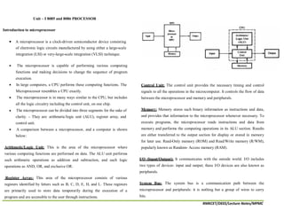
  • 1. RMKCET/DEEE/Lecture Notes/MPMC Unit – I 8085 and 8086 PROCESSOR Introduction to microprocessor A microprocessor is a clock-driven semiconductor device consisting of electronic logic circuits manufactured by using either a large-scale integration (LSI) or very-large-scale integration (VLSI) technique. The microprocessor is capable of performing various computing functions and making decisions to change the sequence of program execution. In large computers, a CPU performs these computing functions. The Microprocessor resembles a CPU exactly. The microprocessor is in many ways similar to the CPU, but includes all the logic circuitry including the control unit, on one chip. The microprocessor can be divided into three segments for the sake of clarity. – They are: arithmetic/logic unit (ALU), register array, and control unit. A comparison between a microprocessor, and a computer is shown below: Arithmetic/Logic Unit: This is the area of the microprocessor where various computing functions are performed on data. The ALU unit performs such arithmetic operations as addition and subtraction, and such logic operations as AND, OR, and exclusive OR. Register Array: This area of the microprocessor consists of various registers identified by letters such as B, C, D, E, H, and L. These registers are primarily used to store data temporarily during the execution of a program and are accessible to the user through instructions. Control Unit: The control unit provides the necessary timing and control signals to all the operations in the microcomputer. It controls the flow of data between the microprocessor and memory and peripherals. Memory: Memory stores such binary information as instructions and data, and provides that information to the microprocessor whenever necessary. To execute programs, the microprocessor reads instructions and data from memory and performs the computing operations in its ALU section. Results are either transferred to the output section for display or stored in memory for later use. Read-Only memory (ROM) and Read/Write memory (R/WM), popularly known as Random- Access memory (RAM). I/O (Input/Output): It communicates with the outside world. I/O includes two types of devices: input and output; these I/O devices are also known as peripherals. System Bus: The system bus is a communication path between the microprocessor and peripherals: it is nothing but a group of wires to carry bits.
  • 2. RMKCET/DEEE/Lecture Notes/MPMC 8085 Microprocessor The salient features of 8085 µp are: It is a 8 bit microprocessor. It is manufactured with N-MOS technology. It has 16-bit address bus and hence can address up to 216 = 65536 bytes (64KB) memory locations through A -A . 0 15 The first 8 lines of address bus and 8 lines of data bus are multiplexed AD – AD . 0 7 Data bus is a group of 8 lines D 0 – D . 7 It supports external interrupt request. A 16 bit program counter (PC) A 16 bit stack pointer (SP) Six 8-bit general purpose register arranged in pairs: BC, DE, HL. It requires a signal +5V power supply and operates at 3.2 MHZ single phase clock. It is enclosed with 40 pins DIP (Dual in line package). Overview of 8085 microprocessor Architecture of INTEL 8085 Intel 8085A is one of the most popular 8-bit microprocessors capable of addressing 64KB of memory and its architecture is simple. The architecture of 8085 includes the ALU, timing and control unit, instruction register and decoder, register array, interrupt control and serial I/O control in a package of 40 pins, requires +5V single power supply and can operate with a 3MHz single phase clock. Figure 1.1 internal architecture of 8085 Arithmetic and logic unit (ALU): The 8085A has a simple 8 bit ALU and it works in coordination with the accumulator, temporary register, five flags, and arithmetic and logic circuits. ALU has the capability of performing several mathematical and logical operations. The temporary register is used to hold the data during an arithmetic/logic operation. Accumulator The accumulator is an 8-bit register that is a part of arithmetic/logic unit (ALU). This register is used to store 8-bit data and to
  • 3. RMKCET/DEEE/Lecture Notes/MPMC perform arithmetic and logical operations. The result of an operation is stored in the accumulator. The accumulator is also identified as register A. Flag register There are five flags in 8085, they are sign flag (S), zero flag (Z) , auxiliary carry flag (AC) , Parity flag (P) and carry flag (CY) the bit position reserved for these flags in the flag register are shown below S – Sign Flag: After the execution of an arithmetic/logic operation, if bit D7 of the result (usually in the accumulator) is 1, the sign flag is set. This flag is used with signed numbers. In a given byte, if D7 is 1,the number will be viewed as a negative number; if it is 0,the number will be considered positive. Z – Zero Flag: The Zero flag is set if the ALU operation results is 0,and the flag is reset if the result is not 0.This flag is modified by the result in the accumulator as well as in the other registers. AC – Auxiliary Carry Flag: In an arithmetic operation, when a carry is generated by digit D3 and passed on to digit D4, the AC flag is set. The Flag is used only internally for the programmer to change the sequence of a program with a jump instruction. P – Parity Flag: After an arithmetic/logic operation, if the result has an even number of 1’s, the flag is set. If it has an odd number of 1’s flag is reset. CY - Carry Flag: If an arithmetic operation results in a carry. The carry flag is set; otherwise it is reset. The carry flag also serves as a borrow flag for subtraction. TIMING AND CONTROL UNIT: This unit synchronizes all the microprocessor operations with the clock and generates the control signals necessary for communication between the microprocessor and peripherals. The control signals and indicate the availability of data on the data bus. INSTRUCTION REGISTER AND DECODER: The Instruction register and decoder are part of the ALU. When an instruction is fetched from memory, it is loaded in the instruction register. The decoder decodes the instruction and establishes the sequence of events to follow. REGISTER ARRAY: The 8085 have six general purpose registers to store eight bit data during program execution. These registers are identified as B, C, D, E, H, and L. They can be combined as register pairs BC, DE, and HL to perform 16 bit operation. The programmer can use these registers to store or copy data into the registers by using data copy instructions. In addition to 6 general purpose register , it has two 16 bit register called stack pointer and program counter Program Counter (PC) This 16-bit register deals with sequencing the execution of instructions. This register is a memory pointer. Memory locations have 16-bit addresses, and that is why this is a 16-bit register. The microprocessor uses this register to sequence the execution of the instructions. The function of the
  • 4. RMKCET/DEEE/Lecture Notes/MPMC program counter is to point to the memory address from which the next byte is to be fetched. When a byte (machine code) is being fetched, the program counter is incremented by one to point to the next memory location Stack Pointer (SP) The stack pointer is also a 16-bit register used as a memory pointer. It points to a memory location in R/W memory, called the stack. The beginning of the stack is defined by loading 16-bit address in the stack pointer. COMMUNICATION LINES: 8085 MPU performs data transfer operation using three sets of communication lines called buses: the address bus, the data bus, and the control bus. ADDRESS BUS: The address bus is a group of 16 lines generally identified as A0 to A15.The address bus is unidirectional i.e. bits flow in one direction from MPU to peripheral devices. The 8085 MPU with its 16 address lines is capable of addressing 216 = 65,536(64K) bytes memory location. DATA BUS: The data bus is a group of 8 lines used for data flow. These lines are bi-directional i.e. data flow in both direction between MPU and peripheral devices. The 8 data lines enable the MPU to manipulate 8bit data ranging from 00 to FF (28 = 256 numbers). The largest number that can appear on the data bus is 11111111(25510). CONTROL BUS: The control bus comprised of various single lines that carry synchronization signals. The MPU uses such lines to provide timing signals. Memory Intel 8085 has three types of memory, they are Programs, data and stack memories Program memory : Program can be a located anywhere in memory. Jump, branch and call instructions use 16-bit addresses, i.e. they can be used to jump/branch anywhere within 64 KB. All jump/branch instructions use absolute addressing. Data memory - the processor always uses 16-bit addresses so that data can be placed anywhere Stack memory is limited only by the size of memory. Stack grows downward. First 64 bytes in a zero memory page should be reserved for vectors used by RST instructions. INTERRUPTS The processor has 5 interrupts. They are presented below in the order of their INTR: It has the lowest priority and is a maskable interrupt. This is also called as hand shake interrupt RST5.5 is a maskable interrupt. When this interrupt is received the processor saves the contents of the PC register into stack and branches to 2CH (hexadecimal) address. RST6.5 is a maskable interrupt When this interrupt is received the processor saves the contents of the PC register into stack and branches to 34H (hexadecimal) address. RST7.5 is a maskable in saves the contents of the PC register into stack and branches to 3CH (hexadecimal) address.
  • 5. RMKCET/DEEE/Lecture Notes/MPMC TRAP is a non-maskable interrupt when this interrupt is received the processor saves the contents of the PC register into stack and branches to 24H (hexadecimal) address. All maskable interrupts can be enabled or disabled using EI and DI instructions RST 5.5, RST6.5 and RST7.5 interrupts can be enabled or disabled individually using SIM instruction. Serial communication Signal SID - Serial Input Data Line: The data on this line is loaded into accumulator bit 7 whenever a RIM instruction is executed SOD – Serial Output Data Line: The SIM instruction loads the value of bit 7 of the accumulator into SOD latch if bit 6 (SOE) of the accumulator is 1. 8085 Pin description. Properties Single + 5V Supply 4 Vectored Interrupts (One is Non Maskable) Serial In/Serial Out Port Decimal, Binary, and Double Precision Arithmetic Direct Addressing Capability to 64K bytes of memory The Intel 8085A is a new generation, complete 8 bit parallel central processing unit (CPU). The 8085A uses a multiplexed data bus. The address is split between the 8bit address bus and the 8bit data bus. Pin Description The following describes the function of each pin: A8 – A15 (Output 3 State) Address Bus; The most significant 8 bits of the memory address or the 8 bits of the I/0 address,3 stated during Hold and Halt modes. AD0 - AD7 (Input/Output 3state) Multiplexed Address/Data Bus; Lower 8 bits of the memory address (or I/0 address) appear on the bus during the first clock cycle of a machine state. It then becomes the data bus during the second and third clock cycles. 3 stated during Hold and Halt modes. Figure 1.2 a pin diagram of 8085
  • 6. RMKCET/DEEE/Lecture Notes/MPMC ALE (Output) Address Latch Enable: It occurs during the first clock cycle of a machine state and enables the address to get latched into the on chip latch of peripherals. The falling edge of ALE is set to guarantee setup and hold times for the address information. ALE can also be used to strobe the status information. ALE is never 3stated. Figure 1.2 b signal diagram of 8085 SO, S1 (Output) RD (Output 3state) READ; indicates the selected memory or I/O device is to be read and that the Data Bus is available for the data transfer. WR (Output 3state) WRITE; indicates the data on the Data Bus is to be written into the selected memory or 1/0 location. READY (Input) If Ready is high during a read or write cycle, it indicates that the memory or peripheral is ready to send or receive data. If Ready is low, the CPU will wait for Ready to go high before completing the read or write cycle. HOLD (Input) HOLD; indicates that another Master is requesting the use of the Address and Data Buses. The CPU, upon receiving the Hold request. Will relinquish the use of buses as soon as the completion of the current machine cycle. Internal processing can continue. The processor can regain the buses only after the Hold is removed. When the Hold is acknowledged, the Address, Data, RD, WR, and IO/M lines are 3stated HLDA (Output) HOLD ACKNOWLEDGE; indicates that the CPU has received the S1 S0 Data Bus Status. Encoded status of the bus cycle Hold request and that it will relinquish the buses in the next clock cycle. HLDA goes low after the Hold request is removed. The CPU takes the buses 0 0 Halt one half clock cycle after HLDA goes low. 0 1 Write INTR (Input) 1 0 Read INTERRUPT REQUEST; is used as a general purpose interrupt. It is 1 1 fetch sampled only during the next to the last clock cycle of the instruction. If it is
  • 7. RMKCET/DEEE/Lecture Notes/MPMC active, the Program Counter (PC) will be inhibited from incrementing and an INTA will be issued. During this cycle a RESTART or CALL instruction can be inserted to jump to the interrupt service routine. The INTR is enabled and disabled by software. It is disabled by Reset and immediately after an interrupt is accepted. INTA (Output) INTERRUPT ACKNOWLEDGE; is used instead of (and has the same timing as) RD during the Instruction cycle after an INTR is accepted. It can be used to activate the 8259 Interrupt chip or some other interrupt port. RST 5.5 RST 6.5 - (Inputs) RST 7.5 RESTART INTERRUPTS; These three inputs have the same timing as INTR except they cause an internal RESTART to be automatically inserted. RST 7.5 ---------- Highest Priority RST 6.5 RST 5.5 ----------Lowest Priority The priority of these interrupts is ordered as shown above. These interrupts have a higher priority than the INTR. TRAP (Input) Trap interrupt is a non maskable restart interrupt. It is recognized at the same time as INTR. It is unaffected by any mask or Interrupt Enable. It has the highest priority of any interrupt. RESET IN (Input) Reset sets the Program Counter to zero and resets the Interrupt Enable and HLDA flip-flops. None of the other flags or registers (except the instruction register) are affected The CPU is held in the reset condition as long as Reset is applied. RESET OUT (Output) Indicates CPU is being reset. Can be used as a system RESET. The signal is synchronized to the processor clock. X1, X2 (Input) Crystal or R/C network connections to set the internal clock generator X1 can also be an external clock input instead of a crystal. The input frequency is divided by 2 to give the internal operating frequency. CLK (Output) Clock Output for use as a system clock when a crystal or R/ C network is used as an input to the CPU. The period of CLK is twice the X1, X2 input period. IO/M (Output) IO/M indicates whether the Read/Write is to memory or l/O Tristated during Hold and Halt modes. SID (Input) Serial input data line The data on this line is loaded into accumulator bit 7 whenever a RIM instruction is executed. SOD (output) Serial output data line. The output SOD is set or reset as specified by the SIM instruction. Vcc +5 volt supply. Vss Ground Reference.
  • 8. RMKCET/DEEE/Lecture Notes/MPMC I/O and Memory interfacing examples EXAMPLE-1 Consider a system in which the full memory space 64kb is utilized for EPROM memory. Interface the EPROM with 8085 processor. The memory capacity is 64 Kbytes. i.e. 2n = 64 x 1000 bytes where n = address lines. So, n = 16. In this system the entire 16 address lines of the processor are connected to address input pins of memory IC in order to address the internal locations of memory. The chip select (CS) pin of EPROM is permanently tied to logic low (i.e., tied to ground). Since the processor is connected to EPROM, the active low RD pin is connected to active low output enable pin of EPROM. The range of address for EPROM is 0000H to FFFFH. EXAMPLE-2 Consider a system in which the available 64kb memory space is equally divided between EPROM and RAM. Interface the EPROM and RAM with 8085 processor. Implement 32kb memory capacity of EPROM using single IC 27256. 32kb RAM capacity is implemented using single IC 62256. The 32kb memory requires 15 address lines and so the address lines A0 - A14 of the processor are connected to 15 address pins of both EPROM and RAM. The unused address line A15 is used as to chip select. If A15 is 1, it select RAM and If A15 is 0, it select EPROM. Inverter is used for selecting the memory. The memory used is both Ram and EPROM, so the low RD and WR pins of processor are connected to low WE and OE pins of memory respectively. The address range of EPROM will be 0000H to 7FFFH and that of RAM will be 8000H to FFFFH.
  • 9. RMKCET/DEEE/Lecture Notes/MPMC EXAMPLE-3 Consider a system in which 32kb memory space is implemented using four numbers of 8kb memory. Interface the EPROM and RAM with 8085 processor. The total memory capacity is 32Kb. So, let two number of 8kb n memory be EPROM and the remaining two numbers be RAM. Each 8kb memory requires 13 address lines and so the address lines A0- A12 of the processor are connected to 13 address pins of all the memory. These four chip select signals can be used to select one of the four memory IC at any one time. The address line A15 is used as enable for decoder. The simplified schematic memory organization is shown. The address allotted to each memory IC is shown in following table. Fig - Interfacing 16Kb EPROM and 16Kb RAM with 8085 The address lines and A13 - A14 can be decoded using a 2-to-4 decoder to generate four chip select signals. EXAMPLE-4 Consider a system in which the 64kb memory space is implemented using eight numbers of 8kb memory. Interface the EPROM and RAM with 8085 processor
  • 10. The total memory capacity is 64Kb. So, let 3 numbers of 8Kb EPROM and 5 numbers of 8Kb RAM Each 8kb memory requires 13 address lines. So the address line A0 - A12 of the processor are connected to 13address pins of all the memory lCs. RMKCET/DEEE/Lecture Notes/MPMC
  • 11. RMKCET/DEEE/Lecture Notes/MPMC Fig - Interfacing 4 no. 8Kb EPROM and 4 no. 8Kb RAM with 8085 The address lines A13, A14 and A]5 are decoded using a 3-to-8 coder to generate eight chip select signals. These eight chip select signals can be used to select one of the eight memories at any one time. The memory interfacing is shown in following figure. The address allocation for Interfacing 4 no. 8Kb EPROM and 4 no. 8Kb RAM with 8085 is, I/O INTERFACING WITH 8085 Example 1: A system requires 16kb EPROM and 16kb RAM. Also the system has 2 numbers of 8255, one number of 8279, one number of 8251 and one number of 8254. (8255 - Programmable peripheral interface; 8279-Keyboard/display controller, 8251 - USART and 8254 - Timer). Draw the Interface diagram. Allocate addresses to all the devices. The peripheral IC should be I/O mapped. The I/O devices in the system should be mapped by standard I/O mapping. Hence separate decoders can be used to generate chip select signals for memory IC and peripheral IC's. For 16kb EPROM, we can provide 2 numbers of 2764(8k x 8) EPROM. For 16kb RAM we can provide 2 numbers of 6264 (8k x 8) RAM. The 8kb memories require 13 address lines. Hence the address lines A0 - A12 are used for selecting the memory locations. The unused address lines A13, A14 and A15 are used as input to decoder 74LS138 (3-to-8-deeoder) of memory IC. The logic low enables of this decoder are tied to IO/ M(low) of 8085, so that this decoder is enabled for memory read/write operation. The other enable pins of decoder are tied to appropriate logic levels permanently. The 4-outputs of the decoder are used to select memory lCs and the remaining 4 are kept for future expansion. The EPROM is mapped in the beginning of memory space from 0000H to 3FFF. The RAM is mapped at the end of memory space from C000 to FFFFH.
  • 12. RMKCET/DEEE/Lecture Notes/MPMC The address lines A13, A14 and A15 are logically ORed and applied to low enable of I/O decoder. The logic high enable of I/O decoder is tied to IO / M(low) signal of 8085, so that this decoder is enabled for I/O read/write operation. There are five peripheral IC's to be interfaced to the system. The chip-select signals for these IC's are given through another 3-to-8 decoder 74LS138 (I/O decoder). The input to this decoder is A11, A12 and A13 Fig - Internal address of 8255 Fig - Memory and I/O Port Interfacing with 8085
  • 13. RMKCET/DEEE/Lecture Notes/MPMC INTERRUPT STRUCTURE Interrupt is signals send by an external device to the processor, to request the processor to perform a particular task or work. Mainly in the microprocessor based system the interrupts are used for data transfer between the peripheral and the microprocessor. The processor will check the interrupts always at the 2nd T-state of last machine cycle. If there is any interrupt it accept the interrupt and send the INTA (active low) signal to the peripheral. The vectored address of particular interrupt is stored in program counter. The processor executes an interrupt service routine (ISR) addressed in program counter. It returned to main program by RET instruction. Types of Interrupts: It supports two types of interrupts. 1. Hardware interrupts 2. Software interrupts Software interrupts: The software interrupts are program instructions. These instructions are inserted at desired locations in a program. The 8085 has eight software interrupts from RST 0 to RST 7. The vector address for these interrupts can be calculated as follows. The Table shows the vector addresses of all interrupts. Hardware interrupts: An external device initiates the hardware interrupts and placing an appropriate signal at the interrupt pin of the processor. If the interrupt is accepted then the processor executes an interrupt service routine. The 8085 has five hardware interrupts (1) TRAP (2) RST 7.5 (3) RST 6.5 4) RST 5.5 5) INTR
  • 14. RMKCET/DEEE/Lecture Notes/MPMC TRAP: This interrupt is a non-maskable interrupt. It is unaffected by any mask or interrupt enable. TRAP has the highest priority and vectored interrupt. TRAP interrupt is edge and level triggered. This means hat the TRAP must go high and remain high until it is acknowledged. In sudden power failure, it executes a ISR and send the data from main memory to backup memory. The signal, which overrides the TRAP, is HOLD signal. (i.e., If the processor receives HOLD and TRAP at the same time then HOLD is recognized first and then TRAP is recognized). There are two ways to clear TRAP interrupt. 1. By resetting microprocessor (External signal) 2. By giving a high TRAP ACKNOWLEDGE (Internal signal) RST 7.5: The RST 7.5 interrupt is a maskable interrupt. It has the second highest priority. It is edge sensitive. ie. Input goes to high and no need to maintain high state until it recognized. Maskable interrupt. It is disabled by, 1. DI instruction 2. System or processor reset. 3. After reorganization of interrupt. Enabled by EI instruction. RST 6.5 and 5.5: The RST 6.5 and RST 5.5 both are level triggered. ie. Inputs goes to high and stay high until it recognized. Maskable interrupt. It is disabled by, 1.DI, SIM instruction 2.System or processor reset. 3. after reorganization of interrupt. Enabled by EI instruction. The RST 6.5 has the third priority whereas RST 5.5 has the fourth priority. INTR: INTR is a maskable interrupt. It is disabled by, 1.DI, SIM instruction 2.System or processor reset. 3.After reorganization of interrupt. Enabled by EI instruction. Non- vectored interrupt. After receiving INTA (active low) signal, it has to supply the address of ISR. It has lowest priority. It is a level sensitive interrupts. ie. Input goes to high and it is necessary to maintain high state until it recognized. The following sequence of events occurs when INTR signal goes high.
  • 15. RMKCET/DEEE/Lecture Notes/MPMC 1. The 8085 checks the status of INTR signal during execution of each instruction. 2. If INTR signal is high, then 8085 complete its current instruction and sends active low interrupt acknowledge signal, if the interrupt is enabled. 3. In response to the acknowledge signal, external logic places an instruction OPCODE on the data bus. In the case of multibyte instruction, additional interrupt acknowledge machine cycles are generated by the 8085 to transfer the additional bytes into the microprocessor. 4. On receiving the instruction, the 8085 save the address of next instruction on stack and execute received instruction. SIM and RIM for interrupts: The 8085 provide additional masking facility for RST 7.5, RST 6.5 and RST 5.5 using SIM instruction. The format of the 8-bit data is shown below. The status of these interrupts can be read by executing RIM instruction. The masking or unmasking of RST 7.5, RST 6.5 and RST 5.5 interrupts can be performed by moving an 8-bit data to accumulator and then executing SIM instruction. The status of pending interrupts can be read from accumulator after executing RIM instruction. When RIM instruction is executed an 8-bit data is loaded in accumulator, which can be interpreted as shown in fig.
  • 16. RMKCET/DEEE/Lecture Notes/MPMC Timing Diagram of 8085 Microprocessor Timing Diagram is a graphical representation. It represents the execution time taken by each instruction in a graphical format. The execution time is represented in T-states. Instruction Cycle: The time required to execute an instruction is called instruction cycle. Machine Cycle: The time required to access the memory or input/output devices is called machine cycle. T-State:  The machine cycle and instruction cycle takes multiple clock periods.  A portion of an operation carried out in one system clock period is called as T-state. MACHINE CYCLES OF 8085: The 8085 microprocessor has 5 (seven) basic machine cycles. They are 1. Opcode fetch cycle (4T) 2. Memory read cycle (3 T) 3. Memory write cycle (3 T) 4. I/O read cycle (3 T) 5. I/O write cycle (3 T)  Each instruction of the 8085 processor consists of one to five machine cycles, i.e., when the 8085 processor executes an instruction, it will execute some of the machine cycles in a specific order.  The processor takes a definite time to execute the machine cycles. The time taken by the processor to execute a machine cycle is expressed in T-states.  One T-state is equal to the time period of the internal clock signal of the processor.  The T-state starts at the falling edge of a clock. Opcode fetch machine cycle of 8085 :  Each instruction of the processor has one byte opcode.  The opcodes are stored in memory. So, the processor executes the opcode fetch machine cycle to fetch the opcode from memory.
  • 17. RMKCET/DEEE/Lecture Notes/MPMC  Hence, every instruction starts with opcode fetch machine cycle.  The time taken by the processor to execute the opcode fetch cycle is 4T.  In this time, the first, 3 T-states are used for fetching the opcode from memory and the remaining T-states are used for internal operations by the processor. Memory Read Machine Cycle of 8085:  The memory read machine cycle is executed by the processor to read a data byte from memory.  The processor takes 3T states to execute this cycle.  The instructions which have more than one byte word size will use the machine cycle after the opcode fetch machine cycle Memory Write Machine Cycle of 8085:  The memory write machine cycle is executed by the processor to write a data byte in a memory location.  The processor takes,3T states to execute this machine cycle. I/O Read Cycle of 8085:  The I/O Read cycle is executed by the processor to read a data byte from I/O port or from the peripheral, which is I/O, mapped in the system.  The processor takes 3T states to execute this machine cycle.  The IN instruction uses this machine cycle during the execution
  • 18. RMKCET/DEEE/Lecture Notes/MPMC I/O Write Cycle of 8085:  The I/O write machine cycle is executed by the processor to write a data byte in the I/O port or to a peripheral, which is I/O, mapped in the system.  The processor takes, 3T states to execute this machine cycle Timing diagram for STA 526AH.  STA means Store Accumulator -The contents of the accumulator is stored in the specified address(526A).  The opcode of the STA instruction is said to be 32H. It is fetched from the memory 41FFH(see fig). - OF machine cycle  Then the lower order memory address is read(6A). – Memory R e a d M a c h i n e C y c l e
  • 19. RMKCET/DEEE/Lecture Notes/MPMC  Read the higher order memory address (52).- Memory Read Machine Cycle  The combination of both the addresses are considered and the content from accumulator is written in 526A. – Memory Write Machine Cycle  Assume the memory address for the instruction and let the content of accumulator is C7H. So, C7H from accumulator is now stored in 526A Timing diagram for IN C0H.  Fetching the Opcode DBH from the memory 4125H.  Read the port address C0H from 4126H.  Read the content of port C0H and send it to the accumulator.  Let the content of port is 5EH.
  • 20. RMKCET/DEEE/Lecture Notes/MPMC Timing diagram for MVI B, 43H.  Fetching the Opcode 06H from the memory 2000H. (OF machine cycle)  Read (move) the data 43H from memory 2001H. (memory read) Timing diagram for INR M  Fetching the Opcode 34H from the memory 4105H. (OF cycle)  Let the memory address (M) be 4250H. (MR cycle -To read Memory address and data)  Let the content of that memory is 12H.  Increment the memory content from 12H to 13H. (MW machine cycle)
  • 25. HLT
  • 27. INSTRUCTION SET OF 8085 UNIT II Programming of 8085 processor
  • 28. Instruction Set of 8085  An instruction is a binary pattern designed inside a microprocessor to perform a specific function.  The entire group of instructions that a microprocessor supports is called Instruction Set.  8085 has 246 instructions.  Each instruction is represented by an 8-bit binary value.  These 8-bits of binary value is called Op-Code or Instruction Byte.
  • 29. Classification of Instruction Set  DataTransfer Instruction  Data Manipulation instruction  Arithmetic Instructions  Logical Instructions  Branching Instructions  Control Instructions
  • 30. 1.DataTransfer Instructions  These instructions move data between registers, or between memory and registers.  These instructions copy data from source to destination(without changing the original data ).
  • 31. MOV-Copy from source to destination Opcode Operand MOV Rd, Rs M, Rs Rd, M  This instruction copies the contents of the source register into the destination register. (contents of the source register are not altered)  If one of the operands is a memory location, its location is specified by the contents of the HL registers.  Example: MOV B, C or MOV B, M
  • 32. A 20 BA 20 B BEFORE EXECUTION AFTER EXECUTION MOV B,A A 20 B 20
  • 33. BEFORE EXECUTION AFTER EXECUTION MOV M,B A F B 30 C D E H 41 L 01 xx 4100 xx 4101 xx 4102 xx 4103 A F B 30 C D E H 41 L 01 xx 4100 xx 4101 xx 4102 xx 4103 xx 4100 30 4101 xx 4102 xx 4103 Register array Memory location Register array Memory location
  • 34. BEFORE EXECUTION AFTER EXECUTION MOV B,M A F B 30 C D E H 41 L 02 xx 4100 xx 4101 4A 4102 xx 4103 A F B C D E H 41 L 01 xx 4100 xx 4101 4A 4102 xx 4103 A F B 4A C D E H 41 L 01 Register array Memory location Register array Memory location
  • 35. MVI-Move immediate 8-bit Opcode Operand MVI Rd, Data M, Data  The 8-bit data is stored in the destination register or memory.  If the operand is a memory location, its location is specified by the contents of the H-L registers.  Example: MVI B, 60H or MVI M, 40H
  • 36. A F B C D E H L A F B C D E H L AFTER EXECUTIONBEFORE EXECUTION MVI B,60H A F B 60H C D E H L Register array Register array
  • 37. A F B C D E H 41 L 05 A F B C D E H 41 L 05 AFTER EXECUTIONBEFORE EXECUTION MVI M,60H xx 4102 xx 4103 xx 4104 xx 4105 Memory Location xx 4102 xx 4103 xx 4104 xx 4105 Memory Location xx 4102 xx 4103 xx 4104 60H 4105
  • 38. LDA-Load accumulator Opcode Operand LDA 16-bit address  The contents of a memory location, specified by a 16-bit address in the operand, are copied to the accumulator.  The contents of the source are not altered.  Example: LDA 4000H
  • 39. A A AFTER EXECUTIONBEFORE EXECUTION LDA 4000H xx 3FFFH DA 4000H xx 4001H xx 4002H Memory Location xx 3FFFH DA 4000H xx 4001H xx 4002H Memory Location A DA
  • 40. STA-Store accumulator direct Opcode Operand STA 16-bit address  The contents of accumulator are copied into the memory location specified by the operand.  Example: STA 4000H
  • 41. A BE A BE AFTER EXECUTIONBEFORE EXECUTION STA 4000H xx 3FFFH DA 4000H xx 4001H xx 4002H Memory Location xx 3FFFH DA 4000H xx 4001H xx 4002H Memory Location xx 3FFFH BE 4000H xx 4001H xx 4002H
  • 42. LDAX-Load accumulator indirect Opcode Operand LDAX B/D Register Pair  The contents of the designated register pair point to a memory location.  This instruction copies the contents of that memory location into the accumulator.  The contents of either the register pair or the memory location are not altered.  Example: LDAX D
  • 43. AFTER EXECUTIONBEFORE EXECUTION xx 3FFFH xx 4000H xx 4001H 80H 4002H Memory Location LDAX D A F B C D 40 E 02 H L xx 3FFFH xx 4000H xx 4001H 80H 4002H Memory Location A F B C D 40 E 02 H L A 80H F B C D 40 E 02 H L
  • 44. STAX-Store accumulator indirect Opcode Operand STAX Reg. pair  The contents of accumulator are copied into the memory location specified by the contents of the register pair.  Example: STAX B
  • 45. AFTER EXECUTIONBEFORE EXECUTION xx 7FFFH xx 8000H xx 8001H xx 8002H Memory Location STAX B A F0H F B 80 C 00 D E H L xx 7FFFH xx 8000H xx 8001H 80H 8002H Memory Location A F0H F B 80 C 00 D E H L xx 7FFFH F0H 8000H xx 8001H 80H 8002H
  • 46. LXI-Load register pair immediate Opcode Operand LXI Reg. pair, 16-bit data  This instruction loads 16-bit data in the register pair.  Example: LXI H, 4001 H
  • 47. AFTER EXECUTIONBEFORE EXECUTION LXI H, 323A A F B C D E H xx L xx 32 3A A F B C D E H xx L xx A F B C D E H xx L 3A A F B C D E H 32 L 3A
  • 48. LHLD-Load H and L registers direct Opcode Operand LHLD 16-bit address  This instruction copies the contents of memory location pointed out by 16-bit address into register L.  It copies the contents of next memory location into register H.  Example: LHLD 4100 H
  • 49. AFTER EXECUTIONBEFORE EXECUTION FF 41FFH 7A 4200H 7B 4201H 80 4202H Memory Location LHLD 4200 A F B C D xx E xx H xx L xx FF 41FFH 7A 4200H 7B 4201H 80 4202H Memory Location A F B C D xx E xx H xx L xx A F B C D xx E xx H xx L 7A A F B C D xx E xx H 7B L 7A
  • 50. SHLD-Store H and L registers direct Opcode Operand SHLD 16-bit address  The contents of register L are stored into memory location specified by the 16-bit address.  The contents of register H are stored into the next memory location.  Example: SHLD 2550H
  • 51. AFTER EXECUTIONBEFORE EXECUTION FF 41FFH 7A 4200H 7B 4201H 80 4202H Memory Location SHLD 4200 A F B C D xx E xx H AB L CD FF 41FFH 7A 4200H 7B 4201H 80 4202H Memory Location A F B C D xx E xx H AB L CD FF 41FFH CD 4200H 7B 4201H 80 4202H FF 41FFH CD 4200H AB 4201H 80 4202H
  • 52. XCHG-Exchange H and L with D and E Opcode Operand XCHG None  The contents of register H are exchanged with the contents of register D.  The contents of register L are exchanged with the contents of register E.  Example: XCHG
  • 53. D 20 E 40 H 70 L 80 BEFORE EXECUTION AFTER EXECUTION XCHG D 70 E 80 H 20 L 40
  • 54. SPHL-Copy H and L registers to the stack pointer Opcode Operand SPHL None  This instruction loads the contents of H-L pair into SP.  Example: SPHL
  • 55. H 25 L 00 SP 16 bit register (XXXX) BEFORE EXECUTION AFTER EXECUTION SPHL SP 2500H H 25 L 00
  • 56. XTHL-Exchange H and L with top of stack Opcode Operand XTHL None  The contents of L register are exchanged with the location pointed out by the contents of the SP.  The contents of H register are exchanged with the next location (SP + 1).  Example: XTHL
  • 57. H 30 L 40 SP 2700 BEFORE EXECUTION AFTER EXECUTIONXTHL L=SP H=(SP+1) 1A 2700H 2B 2701H 3B 2702H 4C 2703H SP Top of the Stack H 30 L 40 SP 2700 1A 2700H 2B 2701H 3B 2702H 4C 2703H H 2B L 40 1A 2700H 30 2701H 3B 2702H 4C 2703H H 2B L 1A 40 2700H 30 2701H 3B 2702H 4C 2703H Stack memory Stack memory
  • 58. Opcode Operand Description PCHL None Load program counter with H- L contents  The contents of registers H and L are copied into the program counter (PC).  The contents of H are placed as the high-order byte and the contents of L as the low-order byte.  Example: PCHL
  • 59. PUSH-Push register pair onto stack Opcode Operand PUSH Reg. pair  The contents of register pair are copied onto stack.  SP is decremented and the contents of high-order registers (B, D, H,A) are copied into stack.  SP is again decremented and the contents of low-order registers (C, E, L, Flags) are copied into stack.  Example: PUSH B
  • 61. POP- Pop stack to register pair Opcode Operand POP Reg. pair  The contents of top of stack are copied into register pair.  The contents of location pointed out by SP are copied to the low-order register (C, E, L, Flags).  SP is incremented and the contents of location are copied to the high-order register (B, D, H,A).  Example: POP H
  • 62. POP H
  • 63. IN- Copy data to accumulator from a port with 8-bit address Opcode Operand IN 8-bit port address  The contents of I/O port are copied into accumulator.  Example: IN 8C H
  • 64. 10 A 10 A 10 BEFORE EXECUTION AFTER EXECUTION IN 80H PORT 80H PORT 80H
  • 65. OUT- Copy data from accumulator to a port with 8-bit address Opcode Operand OUT 8-bit port address  The contents of accumulator are copied into the I/O port.  Example: OUT 78H
  • 66. 10 A 40 40 A 40 BEFORE EXECUTION AFTER EXECUTION OUT 50H PORT 50H PORT 50H
  • 68. Syllabus UNIT III 8051 MICRO CONTROLLER Hardware Architecture, pinouts – Functional Building Blocks of Processor – Memory organization – I/O ports and data transfer concepts– Timing Diagram – Interrupts- Data Transfer, Manipulation, Control Algorithms& I/O instructions, Comparison to Programming concepts with 8085 8051 Microcontroller 2
  • 69. Topics to be covered • CPU Operation – Features of 8051 – Block diagram – 8051 architecture – PIN diagram • Peripheral overview – Interrupt – Timers – Parallel port inputs and outputs – Serial port 8051 Microcontroller 3
  • 72. Why do we need to learn Microprocessors/controllers? • The microprocessor is the core of computer systems. • Nowadays many communication, digital entertainment, portable devices, are controlled by them. • A designer should know what types of components he needs, ways to reduce production costs and product reliable. 8051 Microcontroller 6
  • 73. The necessary tools for a microprocessor/controller 1. CPU: Central Processing Unit 2. I/O: Input /Output 3. Bus: Address bus & Data bus 4. Memory: RAM & ROM 5. Timer 6. Interrupt 7. Serial Port 8. Parallel Port 8051 Microcontroller 7
  • 74. Microprocessors • CPU for Computers • No RAM, ROM, I/O on CPU chip itself • Example: Intel's 8085, x86, Motorola’s 680x0 8051 Microcontroller 8
  • 75. Microcontroller • A smaller computer • On-chip RAM, ROM, I/O ports... • Example: Motorola’s 6811, Intel’s 8051, Zilog’s Z8 and PIC 8051 Microcontroller 9
  • 76. Microprocessor vs. Microcontroller Microprocessor • CPU is stand-alone, RAM, ROM, I/O, timer are separate • Designer can decide on the amount of ROM, RAM and I/O ports. • Expansive • Versatility • General-purpose Microcontroller • CPU, RAM, ROM, I/O and timer are all on a single chip • Fix amount of on-chip ROM, RAM, I/O ports • For applications in which cost, power and space are critical • Not Expansive • Single-purpose 8051 Microcontroller 10
  • 77. Microcontrollers for Embedded Systems • Home – Appliances, intercom, telephones, security systems, garage door openers, answering machines, fax machines, home computers, TVs, cable TV tuner, VCR, camcorder, remote controls, video games, cellular phones, musical instruments, sewing machines, lighting control, paging, camera, pinball machines, toys, exercise equipment etc. • Office – Telephones, computers, security systems, fax machines, microwave, copier, laser printer, color printer, paging etc. • Auto – Trip computer, engine control, air bag, ABS, instrumentation, security system, transmission control, entertainment, climate control, cellular phone, keyless entry 8051 Microcontroller 11
  • 78. Choosing a Microcontroller • 8-bit microcontrollers – Motorola’s 6811 – Intel’s 8051 – Zilog’s Z8 – Microchip’s PIC • There are also 16-bit and 32-bit microcontrollers made by various chip makers 8051 Microcontroller 12
  • 79. Criteria for Choosing a Microcontroller • Meeting the computing needs of the task at hand efficiently and cost effectively – Speed – Packaging – Power consumption – The amount of RAM and ROM on chip – The number of I/O pins and the timer on chip – How easy to upgrade to higher performance or lower power- consumption versions – Cost per unit 8051 Microcontroller 13
  • 80. Criteria for Choosing a Microcontroller • Availability of software development tools, such as compilers, assemblers, and debuggers • Wide availability and reliable sources of the microcontroller – The 8051 family has the largest number of diversified (multiple source) suppliers • Intel (original) • Atmel • Philips/Signetics • AMD • Infineon (formerly Siemens) • Matra • Dallas Semiconductor/Maxim 8051 Microcontroller 14
  • 81. 8051 CPU Operation 1. Features 2. Pin Diagram 3. Block Diagram 8051 Microcontroller 15
  • 82. 8051 Microcontroller • Intel introduced 8051, referred as MCS- 51, in 1981. • The 8051 is an 8-bit processor – The CPU can work on only 8 bits of data at a time • The 8051 became widely popular after allowing other manufactures to make and market any flavor of the 8051. 8051 Microcontroller 16
  • 83. 8051 Family • The 8051 is a subset of the 8052 • The 8031 is a ROM-less 8051 – Add external ROM to it – You lose two ports, and leave only 2 ports for I/O operations 8051 Microcontroller 17
  • 84. 8051 Features • 64KB Program Memory address space • 64KB Data Memory address space • 4K bytes of on-chip Program Memory • 128 bytes of on-chip Data RAM • 32 bidirectional and individually addressable I/0 lines • Two 16-bit timer/counters • Full duplex UART • 6-source/5-vector interrupt structure with two priority levels • On-chip clock oscillator 8051 Microcontroller 18
  • 85. Pin Description of the 8051 • 8051 family members (e.g., 8751, 89C51, 89C52, DS89C4x0) – Have 40 pins dedicated for various functions such as I/O, RD, WR, address, data, and interrupts. – Come in different packages, such as • DIP(dual in-line package), • QFP(quad flat package), and • LLC(leadless chip carrier) • Some companies provide a 20-pin version of the 8051 with a reduced number of I/O ports for less demanding applications 8051 Microcontroller 19
  • 86. Interrupt Control CPU 4K ROM 128 B RAM OSC Bus Control 4 I/O Ports Serial Port Timer 1 Timer 0 General Block Diagram of 8051 TXD RXD P0 P1 P2 P3
  • 87. Detailed Block Diagram 8051 Microcontroller 21
  • 88. Pin Diagram of the 8051 8051 Microcontroller 22
  • 89. XTAL1 and XTAL2 • The 8051 has an on-chip oscillator but requires an external clock to run it – A quartz crystal oscillator is connected to inputs XTAL1 (pin19) and XTAL2 (pin18) – The quartz crystal oscillator also needs two capacitors of 30 pF value 8051 Microcontroller 23
  • 90. XTAL1 and XTAL2 ….. • If you use a frequency source other than a crystal oscillator, such as a TTL oscillator: – It will be connected to XTAL1 – XTAL2 is left unconnected 8051 Microcontroller 24
  • 91. XTAL1 and XTAL2 ….. • The speed of 8051 refers to the maximum oscillator frequency connected to XTAL. • We can observe the frequency on the XTAL2 pin using the oscilloscope. 8051 Microcontroller 25
  • 92. RST • RESET pin is an input and is active high (normally low) • Upon applying a high pulse to this pin, the microcontroller will reset and terminate all activities • This is often referred to as a power-on reset • Activating a power-on reset will cause all values in the registers to be lost 8051 Microcontroller 26
  • 93. RST • In order for the RESET input to be effective, it must have a minimum duration of 2 machine cycles. • In other words, the high pulse must be high for a minimum of 2 machine cycles before it is allowed to go low. 8051 Microcontroller 27
  • 94. EA’ • EA’, “external access’’, is an input pin and must be connected to Vcc or GND • The 8051 family members all come with on- chip ROM to store programs and also have an external code and data memory. • Normally EA pin is connected to Vcc • EA pin must be connected to GND to indicate that the code or data is stored externally. 8051 Microcontroller 28
  • 95. PSEN’ and ALE • PSEN, “program store enable’’, is an output pin • This pin is connected to the OE pin of the external memory. • For External Code Memory, PSEN’ = 0 • For External Data Memory, PSEN’ = 1 • ALE pin is used for demultiplexing the address and data. 8051 Microcontroller 29
  • 96. I/O Port Pins • The four 8-bit I/O ports P0, P1, P2 and P3 each uses 8 pins. • All the ports upon RESET are configured as output, ready to be used as input ports by the external device. 8051 Microcontroller 30
  • 97. Port 0 • Port 0 is also designated as AD0-AD7. • When connecting an 8051 to an external memory, port 0 provides both address and data. • The 8051 multiplexes address and data through port 0 to save pins. • ALE indicates if P0 has address or data. – When ALE=0, it provides data D0-D7 – When ALE=1, it has address A0-A7 8051 Microcontroller 31
  • 98. Port 1 and Port 2 • In 8051-based systems with no external memory connection: – Both P1 and P2 are used as simple I/O. • In 8051-based systems with external memory connections: – Port 2 must be used along with P0 to provide the 16-bit address for the external memory. – P0 provides the lower 8 bits via A0 – A7. – P2 is used for the upper 8 bits of the 16-bit address, designated as A8 – A15, and it cannot be used for I/O. 8051 Microcontroller 32
  • 99. Port 3 • Port 3 can be used as input or output. • Port 3 has the additional function of providing some extremely important signals 8051 Microcontroller 33
  • 100. Pin Description Summary 8051 Microcontroller 34 PIN TYPE NAME AND FUNCTION Vss I Ground: 0 V reference. Vcc I Power Supply: This is the power supply voltage for normal, idle, and power-down operation. P0.0 - P0.7 I/O Port 0: Port 0 is an open-drain, bi-directional I/O port. Port 0 is also the multiplexed low-order address and data bus during accesses to external program and data memory. P1.0 - P1.7 I/O Port 1: Port I is an 8-bit bi-directional I/O port. P2.0 - P2.7 I/O Port 2: Port 2 is an 8-bit bidirectional I/O. Port 2 emits the high order address byte during fetches from external program memory and during accesses to external data memory that use 16 bit addresses. P3.0 - P3.7 I/O Port 3: Port 3 is an 8 bit bidirectional I/O port. Port 3 also serves special features as explained.
  • 101. Pin Description Summary 8051 Microcontroller 35 PIN TYPE NAME AND FUNCTION RST I Reset: A high on this pin for two machine cycles while the oscillator is running, resets the device. ALE O Address Latch Enable: Output pulse for latching the low byte of the address during an access to external memory. PSEN* O Program Store Enable: The read strobe to external program memory. When executing code from the external program memory, PSEN* is activated twice each machine cycle, except that two PSEN* activations are skipped during each access to external data memory. EA*/VPP I External Access Enable/Programming Supply Voltage: EA* must be externally held low to enable the device to fetch code from external program memory locations. If EA* Is held high, the device executes from internal program memory. This pin also receives the programming supply voltage Vpp during Flash programming. (applies for 89c5x MCU's)
  • 103. 8051 Memory Structure External EXT INT 128 SFR External Program Memory Data Memory 64K 64K EA = 0 EA = 1 4K 60K 8051 Microcontroller 37
  • 104. Internal RAM Structure Direct & Indirect Addressing Direct Addressing Only SFR [ Special Function Registers] 128 Byte Internal RAM 8051 Microcontroller 38
  • 105. Special Function Registers [SFR] 8051 Microcontroller 39
  • 106. Program Status Word [PSW] 8051 Microcontroller 40 C AC F0 RS1 RS0 OV F1 P Register Bank Select Carry Auxiliary Carry User Flag 0 Parity User Flag 1 Overflow
  • 107. 8051 instructions that affects flag 8051 Microcontroller 41
  • 108. 128 Byte RAM • There are 128 bytes of RAM in the 8051. – Assigned addresses 00 to 7FH • The 128 bytes are divided into 3 different groups as follows: 1. A total of 32 bytes from locations 00 to 1F hex are set aside for register banks and the stack. 2. A total of 16 bytes from locations 20H to 2FH are set aside for bit-addressable read/write memory. 3. A total of 80 bytes from locations 30H to 7FH are used for read and write storage, called scratch pad. 8051 Microcontroller 42 128 BYTE INTERNAL RAM Register Banks Reg Bank 0 Reg Bank 1 Reg Bank 2 Reg Bank 3 BIT Addressable Area General Purpose Area
  • 109. 8051 RAM with addresses 8051 Microcontroller 43
  • 110. 8051 Register Bank Structure Bank 0 R0 R1 R2 R3 R4 R5 R6 R7Bank 3 R0 R1 R2 R3 R4 R5 R6 R7Bank 2 R0 R1 R2 R3 R4 R5 R6 R7Bank 1 R0 R1 R2 R3 R4 R5 R6 R7 8051 Microcontroller 44
  • 111. 8051 Register Banks with address 8051 Microcontroller 45
  • 112. 8051 Programming Model 8051 Microcontroller 46 The image part with relationship ID rId3 was not found in the file.
  • 113. 8051 Stack • The stack is a section of RAM used by the CPU to store information temporarily. – This information could be data or an address • The register used to access the stack is called the SP (stack pointer) register – The stack pointer in the 8051 is only 8 bit wide, which means that it can take value of 00 to FFH – When the 8051 is powered up, the SP register contains value 07 – RAM location 08 is the first location begin used for the stack by the 8051 8051 Microcontroller 47
  • 114. 8051 Stack • The storing of a CPU register in the stack is called a PUSH – SP is pointing to the last used location of the stack – As we push data onto the stack, the SP is incremented by one – This is different from many microprocessors • Loading the contents of the stack back into a CPU register is called a POP – With every pop, the top byte of the stack is copied to the register specified by the instruction and the stack pointer is decremented once 8051 Microcontroller 48
  • 115. Bit Addressable & Byte Addressable 8051 Microcontroller 49
  • 116. Single bit Instructions 8051 Microcontroller 50
  • 117. Bit Addressable Programming • Example: Find out to which by each of the following bits belongs. Give the address of the RAM byte in hex (a) SETB 42H, (b) CLR 67H, (c) CLR 0FH (d) SETB 28H, (e) CLR 12, (f) SETB 05 8051 Microcontroller 51
  • 118. 8051 Peripheral Overview 1. Timers 2. Serial Port 3. Interrupts 8051 Microcontroller 52
  • 120. 8051 Timer/Counter 8051 Microcontroller 54 OSC ÷12 TLx (8 Bit) / 0C T = / 1C T = INT PIN Gate TR T PIN THx (8 Bit) TFx (1 Bit) INTERRUPT
  • 121. TMOD Register 8051 Microcontroller 55 GATE: When set, timer/counter x is enabled, if INTx pin is high and TRx is set. When cleared, timer/counter x is enabled, if TRx bit set. C/T*: When set, counter operation (input from Tx input pin). When cleared, timer operation (input from internal clock).
  • 122. TMOD Register 8051 Microcontroller 56 The TMOD byte is not bit addressable.
  • 124. 8051 Timer Modes 8051 Microcontroller 58 Timer 0 Mode 3 Mode 2 Mode 1 Mode 0 Mode 2 Mode 1 Mode 0 Timer 1 8051 TIMERS
  • 125. OSC ÷12 TL0 / 0C T = / 1C T = 0INT PIN Gate 0TR 0T PIN TH0 INTERRUPT TIMER 0 TF0
  • 126. TL0 (5 Bit) INTERRUPT TIMER 0 – Mode 0 OSC ÷12 / 0C T = / 1C T = 0INT PIN Gate 0TR 0T PIN TH0 (8 Bit) TF0 13 Bit Timer / Counter Maximum Count = 1FFFh (0001111111111111)
  • 127. TL0 (8 Bit) INTERRUPT TIMER 0 – Mode 1 OSC ÷12 / 0C T = / 1C T = 0INT PIN Gate 0TR 0T PIN TH0 (8 Bit) TF0 16 Bit Timer / Counter Maximum Count = FFFFh (1111111111111111)
  • 128. TH0 (8 Bit) Reload TIMER 0 – Mode 2 8 Bit Timer / Counter with AUTORELOAD TL0 (8 Bit) OSC ÷12 / 0C T = / 1C T = 0INT PIN Gate 0TR 0T PIN TH0 (8 Bit) TF0 INTERRUPT Maximum Count = FFh (11111111)
  • 129. TL0 (8 Bit) INTERRUPT TIMER 0 – Mode 3 OSC ÷12 / 0C T = / 1C T = 0INT PIN Gate 0TR 0T PIN TF0 Two - 8 Bit Timer / Counter OSC ÷12 1TR TH0 (8 Bit) INTERRUPTTF1
  • 130. OSC ÷12 TL1 / 0C T = / 1C T = Gate TH1 INTERRUPT TIMER 1 TF1 1INT PIN 1TR 1T PIN
  • 131. TL1 (5 Bit) INTERRUPT TIMER 1 – Mode 0 OSC ÷12 / 0C T = / 1C T = Gate TH1 (8 Bit) TF1 13 Bit Timer / Counter Maximum Count = 1FFFh (0001111111111111) 1INT PIN 1TR 1T PIN
  • 132. TL1 (8 Bit) INTERRUPT TIMER 1 – Mode 1 OSC ÷12 / 0C T = / 1C T = Gate TH1 (8 Bit) TF1 16 Bit Timer / Counter Maximum Count = FFFFh (1111111111111111) 1INT PIN 1TR 1T PIN
  • 133. TH1 (8 Bit) Reload TIMER 1 – Mode 2 8 Bit Timer / Counter with AUTORELOAD TL1 (8 Bit) OSC ÷12 / 0C T = / 1C T = Gate TH1 (8 Bit) TF1 INTERRUPT Maximum Count = FFh (11111111) 1INT PIN 1TR 1T PIN
  • 134. Programming Timers • Example: Indicate which mode and which timer are selected for each of the following. (a) MOV TMOD, #01H (b) MOV TMOD, #20H (c) MOV TMOD, #12H • Solution: We convert the value from hex to binary. (a) TMOD = 00000001, mode 1 of timer 0 is selected. (b) TMOD = 00100000, mode 2 of timer 1 is selected. (c) TMOD = 00010010, mode 2 of timer 0, and mode 1 of timer 1 are selected. 8051 Microcontroller 68
  • 135. Programming Timers • Find the timer’s clock frequency and its period for various 8051-based system, with the crystal frequency 11.0592 MHz when C/T bit of TMOD is 0. • Solution: 8051 Microcontroller 69 1/12 × 11.0529 MHz = 921.6 MHz; T = 1/921.6 kHz = 1.085 us
  • 137. Basics of Serial Communication • Computers transfer data in two ways: – Parallel: Often 8 or more lines (wire conductors) are used to transfer data to a device that is only a few feet away. – Serial: To transfer to a device located many meters away, the serial method is used. The data is sent one bit at a time. 8051 Microcontroller 71
  • 138. Basics of Serial Communication • Serial data communication uses two methods – Synchronous method transfers a block of data at a time – Asynchronous method transfers a single byte at a time • There are special IC’s made by many manufacturers for serial communications. – UART (universal asynchronous Receiver transmitter) – USART (universal synchronous-asynchronous Receiver- transmitter) 8051 Microcontroller 72
  • 139. Asynchronous – Start & Stop Bit • Asynchronous serial data communication is widely used for character-oriented transmissions – Each character is placed in between start and stop bits, this is called framing. – Block-oriented data transfers use the synchronous method. • The start bit is always one bit, but the stop bit can be one or two bits • The start bit is always a 0 (low) and the stop bit(s) is 1 (high) 8051 Microcontroller 73
  • 140. Asynchronous – Start & Stop Bit 8051 Microcontroller 74
  • 141. Data Transfer Rate • The rate of data transfer in serial data communication is stated in bps (bits per second). • Another widely used terminology for bps is baud rate. – It is modem terminology and is defined as the number of signal changes per second – In modems, there are occasions when a single change of signal transfers several bits of data • As far as the conductor wire is concerned, the baud rate and bps are the same. 8051 Microcontroller 75
  • 142. 8051 Serial Port • Synchronous and Asynchronous • SCON Register is used to Control • Data Transfer through TXd & RXd pins • Some time - Clock through TXd Pin • Four Modes of Operation: 8051 Microcontroller 76 Mode 0 :Synchronous Serial Communication Mode 1 :8-Bit UART with Timer Data Rate Mode 2 :9-Bit UART with Set Data Rate Mode 3 :9-Bit UART with Timer Data Rate
  • 143. Registers related to Serial Communication 1. SBUF Register 2. SCON Register 3. PCON Register 8051 Microcontroller 77
  • 144. SBUF Register • SBUF is an 8-bit register used solely for serial communication. • For a byte data to be transferred via the TxD line, it must be placed in the SBUF register. • The moment a byte is written into SBUF, it is framed with the start and stop bits and transferred serially via the TxD line. • SBUF holds the byte of data when it is received by 8051 RxD line. • When the bits are received serially via RxD, the 8051 deframes it by eliminating the stop and start bits, making a byte out of the data received, and then placing it in SBUF. 8051 Microcontroller 78
  • 145. SBUF Register • Sample Program: 8051 Microcontroller 79
  • 146. SCON Register 8051 Microcontroller 80 SM0 SM1 SM2 REN TB8 RB8 TI RI Enable Multiprocessor Communication Mode Set to Enable Serial Data reception 9th Data Bit Sent in Mode 2,3 9th Data Bit Received in Mode 2,3 Set when Stop bit Txed Set when a Cha- ractor received
  • 147. 8051 Serial Port – Mode 0 The Serial Port in Mode-0 has the following features: 1. Serial data enters and exits through RXD 2. TXD outputs the clock 3. 8 bits are transmitted / received 4. The baud rate is fixed at (1/12) of the oscillator frequency 8051 Microcontroller 81
  • 148. 8051 Serial Port – Mode 1 The Serial Port in Mode-1 has the following features: 1. Serial data enters through RXD 2. Serial data exits through TXD 3. On receive, the stop bit goes into RB8 in SCON 4. 10 bits are transmitted / received 1. Start bit (0) 2. Data bits (8) 3. Stop Bit (1) 5. Baud rate is determined by the Timer 1 over flow rate. 8051 Microcontroller 82
  • 149. 8051 Serial Port – Mode 2 The Serial Port in Mode-2 has the following features: 1. Serial data enters through RXD 2. Serial data exits through TXD 3. 9th data bit (TB8) can be assign value 0 or 1 4. On receive, the 9th data bit goes into RB8 in SCON 5. 11 bits are transmitted / received 1.Start bit (0) 2.Data bits (9) 3.Stop Bit (1) 6. Baud rate is programmable 8051 Microcontroller 83
  • 150. 8051 Serial Port – Mode 3 The Serial Port in Mode-3 has the following features: 1. Serial data enters through RXD 2. Serial data exits through TXD 3. 9th data bit (TB8) can be assign value 0 or 1 4. On receive, the 9th data bit goes into RB8 in SCON 5. 11 bits are transmitted / received 1.Start bit (0) 2.Data bits (9) 3.Stop Bit (1) 6. Baud rate is determined by Timer 1 overflow rate. 8051 Microcontroller 84
  • 151. Programming Serial Data Transmission 1. TMOD register is loaded with the value 20H, indicating the use of timer 1 in mode 2 (8-bit auto-reload) to set baud rate. 2. The TH1 is loaded with one of the values to set baud rate for serial data transfer. 3. The SCON register is loaded with the value 50H, indicating serial mode 1, where an 8- bit data is framed with start and stop bits. 4. TR1 is set to 1 to start timer 1 5. TI is cleared by CLR TI instruction 6. The character byte to be transferred serially is written into SBUF register. 7. The TI flag bit is monitored with the use of instruction JNB TI, xx to see if the character has been transferred completely. 8. To transfer the next byte, go to step 5 8051 Microcontroller 85
  • 152. Programming Serial Data Reception 1. TMOD register is loaded with the value 20H, indicating the use of timer 1 in mode 2 (8-bit auto-reload) to set baud rate. 2. TH1 is loaded to set baud rate 3. The SCON register is loaded with the value 50H, indicating serial mode 1, where an 8- bit data is framed with start and stop bits. 4. TR1 is set to 1 to start timer 1 5. RI is cleared by CLR RI instruction 6. The RI flag bit is monitored with the use of instruction JNB RI, xx to see if an entire character has been received yet 7. When RI is raised, SBUF has the byte, its contents are moved into a safe place. 8. To receive the next character, go to step 5. 8051 Microcontroller 86
  • 153. Doubling Baud Rate • There are two ways to increase the baud rate of data transfer 1. By using a higher frequency crystal 2. By changing a bit in the PCON register • PCON register is an 8-bit register. 8051 Microcontroller 87 •When 8051 is powered up, SMOD is zero •We can set it to high by software and thereby double the baud rate.
  • 154. Doubling Baud Rate (cont…) 8051 Microcontroller 88
  • 156. INTERRUPTS • An interrupt is an external or internal event that interrupts the microcontroller to inform it that a device needs its service • A single microcontroller can serve several devices by two ways: 1. Interrupt 2. Polling 8051 Microcontroller 90
  • 157. Interrupt Vs Polling 1. Interrupts – Whenever any device needs its service, the device notifies the microcontroller by sending it an interrupt signal. – Upon receiving an interrupt signal, the microcontroller interrupts whatever it is doing and serves the device. – The program which is associated with the interrupt is called the interrupt service routine (ISR) or interrupt handler. 2. Polling – The microcontroller continuously monitors the status of a given device. – When the conditions met, it performs the service. – After that, it moves on to monitor the next device until every one is serviced. 8051 Microcontroller 91
  • 158. Interrupt Vs Polling • The polling method is not efficient, since it wastes much of the microcontroller’s time by polling devices that do not need service. • The advantage of interrupts is that the microcontroller can serve many devices (not all at the same time). • Each devices can get the attention of the microcontroller based on the assigned priority. • For the polling method, it is not possible to assign priority since it checks all devices in a round-robin fashion. • The microcontroller can also ignore (mask) a device request for service in Interrupt. 8051 Microcontroller 92
  • 159. Steps in Executing an Interrupt 1. It finishes the instruction it is executing and saves the address of the next instruction (PC) on the stack. 2. It also saves the current status of all the interrupts internally (i.e: not on the stack). 3. It jumps to a fixed location in memory, called the interrupt vector table, that holds the address of the ISR. 4. The microcontroller gets the address of the ISR from the interrupt vector table and jumps to it. 5. It starts to execute the interrupt service subroutine until it reaches the last instruction of the subroutine which is RETI (return from interrupt). 6. Upon executing the RETI instruction, the microcontroller returns to the place where it was interrupted. 8051 Microcontroller 93
  • 160. Six Interrupts in 8051 Six interrupts are allocated as follows: 1. Reset – power-up reset. 2. Two interrupts are set aside for the timers. – one for timer 0 and one for timer 1 3. Two interrupts are set aside for hardware external interrupts. – P3.2 and P3.3 are for the external hardware interrupts INT0 (or EX1), and INT1 (or EX2) 4. Serial communication has a single interrupt that belongs to both receive and transfer. 8051 Microcontroller 94
  • 161. What events can trigger Interrupts? • We can configure the 8051 so that any of the following events will cause an interrupt: – Timer 0 Overflow. – Timer 1 Overflow. – Reception/Transmission of Serial Character. – External Event 0. – External Event 1. • We can configure the 8051 so that when Timer 0 Overflows or when a character is sent/received, the appropriate interrupt handler routines are called. 8051 Microcontroller 95
  • 162. 8051 Interrupt Vectors 8051 Microcontroller 96
  • 163. 8051 Interrupt related Registers • The various registers associated with the use of interrupts are: – TCON - Edge and Type bits for External Interrupts 0/1 – SCON - RI and TI interrupt flags for RS232 – IE - Enable interrupt sources – IP - Specify priority of interrupts 8051 Microcontroller 97
  • 164. Enabling and Disabling an Interrupt • Upon reset, all interrupts are disabled (masked), meaning that none will be responded to by the microcontroller if they are activated. • The interrupts must be enabled by software in order for the microcontroller to respond to them. • There is a register called IE (interrupt enable) that is responsible for enabling (unmasking) and disabling (masking) the interrupts. 8051 Microcontroller 98
  • 165. Interrupt Enable (IE) Register 8051 Microcontroller 99 • EA : Global enable/disable. • --- : Reserved for additional interrupt hardware. • ES : Enable Serial port interrupt. • ET1 : Enable Timer 1 control bit. • EX1 : Enable External 1 interrupt. • ET0 : Enable Timer 0 control bit. • EX0 : Enable External 0 interrupt. MOV IE,#08h or SETB ET1 --
  • 166. Enabling and Disabling an Interrupt • Example: Show the instructions to (a) enable the serial interrupt, timer 0 interrupt, and external hardware interrupt 1 and (b) disable (mask) the timer 0 interrupt, then (c) show how to disable all the interrupts with a single instruction. • Solution: – (a) MOV IE,#10010110B ;enable serial, timer 0, EX1 • Another way to perform the same manipulation is: – SETB IE.7 ;EA=1, global enable – SETB IE.4 ;enable serial interrupt – SETB IE.1 ;enable Timer 0 interrupt – SETB IE.2 ;enable EX1 – (b) CLR IE.1 ;mask (disable) timer 0 interrupt only – (c) CLR IE.7 ;disable all interrupts 8051 Microcontroller 100
  • 167. Interrupt Priority • When the 8051 is powered up, the priorities are assigned according to the following. • In reality, the priority scheme is nothing but an internal polling sequence in which the 8051 polls the interrupts in the sequence listed and responds accordingly. 8051 Microcontroller 101
  • 168. Interrupt Priority • We can alter the sequence of interrupt priority by assigning a higher priority to any one of the interrupts by programming a register called IP (interrupt priority). • To give a higher priority to any of the interrupts, we make the corresponding bit in the IP register high. 8051 Microcontroller 102
  • 169. Interrupt Priority (IP) Register 8051 Microcontroller 103 PS PT1 PX1 PT0 PX0Reserved Serial Port Timer 1 Pin INT 1 Pin Timer 0 Pin INT 0 Pin Priority bit=1 assigns high priority Priority bit=0 assigns low priority
  • 170. 8051 Software Overview 1. Addressing Modes 2. Instruction Set 3. Programming 8051 Microcontroller 104
  • 171. 8051 Addressing Modes • The CPU can access data in various ways, which are called addressing modes 1. Immediate 2. Register 3. Direct 4. Register indirect 5. External Direct 8051 Microcontroller 105
  • 172. Immediate Addressing Mode • The source operand is a constant. • The immediate data must be preceded by the pound sign, “#” • Can load information into any registers, including 16-bit DPTR register – DPTR can also be accessed as two 8-bit registers, the high byte DPH and low byte DPL 8051 Microcontroller 106
  • 173. Register Addressing Mode • Use registers to hold the data to be manipulated. 8051 Microcontroller 107 • The source and destination registers must match in size. MOV DPTR,A will give an error • The movement of data between Rn registers is not allowed MOV R4,R7 is invalid
  • 174. Direct Addressing Mode • It is most often used the direct addressing mode to access RAM locations 30 – 7FH. • The entire 128 bytes of RAM can be accessed. • Contrast this with immediate addressing mode, there is no “#” sign in the operand. 8051 Microcontroller 108
  • 175. SFR Registers & their Addresses MOV 0E0H,#55H ;is the same as MOV A,#55H ;which means load 55H into A (A=55H) MOV 0F0H,#25H ;is the same as MOV B,#25H ;which means load 25H into B (B=25H) MOV 0E0H,R2 ;is the same as MOV A,R2 ;which means copy R2 into A MOV 0F0H,R0 ;is the same as MOV B,R0 ;which means copy R0 into B Intel 8051 Programming 109
  • 176. SFR Addresses ( 1 of 2 ) Intel 8051 Programming 110
  • 177. SFR Addresses ( 2 of 2 ) Intel 8051 Programming 111
  • 179. Stack and Direct Addressing Mode • Only direct addressing mode is allowed for pushing or popping the stack. • PUSH A is invalid. • Pushing the accumulator onto the stack must be coded as PUSH 0E0H. 8051 Microcontroller 113
  • 180. Register Indirect Addressing Mode • A register is used as a pointer to the data. • Only register R0 and R1 are used for this purpose. • R2 – R7 cannot be used to hold the address of an operand located in RAM. • When R0 and R1 hold the addresses of RAM locations, they must be preceded by the “@” sign. 8051 Microcontroller 114
  • 181. Register Indirect Addressing Mode • Write a program to copy the value 55H into RAM memory locations 40H to 41H using (a) direct addressing mode, (b) register indirect addressing mode without a loop, and (c) with a loop. 8051 Microcontroller 115
  • 182. Register Indirect Addressing Mode • The advantage is that it makes accessing data dynamic rather than static as in direct addressing mode. • Looping is not possible in direct addressing mode. • Write a program to clear 16 RAM locations starting at RAM address 60H. 8051 Microcontroller 116
  • 183. External Direct • External Memory is accessed. • There are only two commands that use External Direct addressing mode: – MOVX A, @DPTR MOVX @DPTR, A • DPTR must first be loaded with the address of external memory. 8051 Microcontroller 117
  • 184. 8051 Instruction Set 8051 Microcontroller 118
  • 185. MOV Instruction • MOV destination, source ; copy source to destination. • MOV A,#55H ;load value 55H into reg. A MOV R0,A ;copy contents of A into R0 ;(now A=R0=55H) MOV R1,A ;copy contents of A into R1 ;(now A=R0=R1=55H) MOV R2,A ;copy contents of A into R2 ;(now A=R0=R1=R2=55H) MOV R3,#95H ;load value 95H into R3 ;(now R3=95H) MOV A,R3 ;copy contents of R3 into A ;now A=R3=95H Intel 8051 Programming 119
  • 186. ADD Instruction • ADD A, source ;ADD the source operand to the accumulator • MOV A, #25H ;load 25H into A MOV R2,#34H ;load 34H into R2 ADD A,R2 ;add R2 to accumulator ;(A = A + R2) 120Intel 8051 Programming
  • 187. Structure of Assembly Language ORG 0H ;start (origin) at location 0 MOV R5,#25H ;load 25H into R5 MOV R7,#34H ;load 34H into R7 MOV A,#0 ;load 0 into A ADD A,R5 ;add contents of R5 to A ;now A = A + R5 ADD A,R7 ;add contents of R7 to A ;now A = A + R7 ADD A,#12H ;add to A value 12H ;now A = A + 12H HERE: SJMP HERE ;stay in this loop END ;end of asm source file 121Intel 8051 Programming
  • 188. Data Types & Directives ORG 500H DATA1: DB 28 ;DECIMAL (1C in Hex) DATA2: DB 00110101B ;BINARY (35 in Hex) DATA3: DB 39H ;HEX ORG 510H DATA4: DB “2591” ; ASCII NUMBERS ORG 518H DATA6: DB “My name is Joe” ;ASCII CHARACTERS 122Intel 8051 Programming
  • 189. ADD Instruction and PSW Intel 8051 Programming 123
  • 190. ADD Instruction and PSW Intel 8051 Programming 124
  • 191. Multiplication of Unsigned Numbers MUL AB ; A × B, place 16-bit result in B and A MOV A,#25H ;load 25H to reg. A MOV B,#65H ;load 65H in reg. B MUL AB ;25H * 65H = E99 where B = 0EH and A = 99H Table 6-1:Unsigned Multiplication Summary (MUL AB) Multiplication Operand 1 Operand 2 Result byte × byte A B A=low byte, B=high byte 125Intel 8051 Programming
  • 192. Division of Unsigned Numbers DIV AB ; divide A by B • MOV A,#95H ;load 95 into A • MOV B,#10H ;load 10 into B • DIV AB ;now A = 09 (quotient) and B = 05 (remainder) 8051 Microcontroller 126 Table 6-2:Unsigned Division Summary (DIV AB) Division Numerator Denominator Quotient Remainder byte / byte A B A B
  • 193. Checking an input bit 8051 Microcontroller 127 JNB (jump if no bit) ; JB (jump if bit = 1)
  • 194. Switch Register Banks Intel 8051 Programming 128
  • 195. Pushing onto Stack Intel 8051 Programming 129
  • 196. Popping from Stack Intel 8051 Programming 130
  • 198. Loop inside a Loop (Nested Loop) Intel 8051 Programming 132
  • 199. 8051 Conditional Jump Instructions Intel 8051 Programming 133
  • 200. Conditional Jump Example Intel 8051 Programming 134
  • 201. Conditional Jump Example Intel 8051 Programming 135
  • 202. Unconditional Jump Instructions • All conditional jumps are short jumps – Target address within -128 to +127 of PC • LJMP (long jump): 3-byte instruction – 2-byte target address: 0000 to FFFFH – Original 8051 has only 4KB on-chip ROM • SJMP (short jump): 2-byte instruction – 1-byte relative address: -128 to +127 136Intel 8051 Programming
  • 203. Call Instructions • LCALL (long call): 3-byte instruction – 2-byte address – Target address within 64K-byte range • ACALL (absolute call): 2-byte instruction – 11-bit address – Target address within 2K-byte range 137Intel 8051 Programming
  • 204. Unit IV Peripheral interfacing
  • 205.
  • 206.
  • 207.
  • 208.
  • 209.
  • 210.
  • 211.
  • 212.
  • 213.
  • 214.
  • 215.
  • 216.
  • 217.
  • 218.
  • 219.
  • 220.
  • 221.
  • 222.
  • 223.
  • 224.
  • 225.
  • 226.
  • 227.
  • 228.
  • 229.
  • 230.
  • 231.
  • 232.
  • 233.
  • 234.
  • 235.
  • 236.
  • 237.
  • 238.
  • 239.
  • 240.
  • 241.
  • 242.
  • 243.
  • 244.
  • 245.
  • 246.
  • 247.
  • 248.
  • 249.
  • 250.
  • 251.
  • 252.
  • 253.
  • 254.
  • 255.
  • 256.
  • 257.
  • 258.
  • 259.
  • 260. 8051 has about 111 instructions. These can be grouped into the following categories 1. Arithmetic Instructions 2. Logical Instructions 3. Data Transfer instructions 4. Boolean Variable Instructions 5. Program Branching Instructions The following nomenclatures for register, data, address and variables are used while write instructions. A: Accumulator B: "B" register C: Carry bit Rn: Register R0 - R7 of the currently selected register bank Direct: 8-bit internal direct address for data. The data could be in lower 128bytes of RAM (00 - 7FH) or it could be in the special function register (80 - FFH). @Ri: 8-bit external or internal RAM address available in register R0 or R1. This is used for indirect addressing mode. #data8: Immediate 8-bit data available in the instruction. #data16: Immediate 16-bit data available in the instruction. Addr11: 11-bit destination address for short absolute jump. Used by instructions AJMP & ACALL. Jump range is 2 kbyte (one page). Addr16: 16-bit destination address for long call or long jump. Rel: 2's complement 8-bit offset (one - byte) used for short jump (SJMP) and all conditional jumps. bit: Directly addressed bit in internal RAM or SFR Arithmetic Instructions Mnemonics Description Bytes Instruction Cycles ADD A, Rn A A + Rn 1 1 ADD A, direct A A + (direct) 2 1 ADD A, @Ri A A + @Ri 1 1 ADD A, #data A A + data 2 1 ADDC A, Rn A A + Rn + C 1 1 ADDC A, direct A A + (direct) + C 2 1 ADDC A, @Ri A A + @Ri + C 1 1 ADDC A, #data A A + data + C 2 1 DA A Decimal adjust accumulator 1 1 DIV AB Divide A by B A quotient B remainder 1 4 DEC A A A -1 1 1 DEC Rn Rn Rn - 1 1 1 DEC direct (direct) (direct) - 1 2 1 DEC @Ri @Ri @Ri - 1 1 1 INC A A A+1 1 1 INC Rn Rn Rn + 1 1 1 INC direct (direct) (direct) + 1 2 1 INC @Ri @Ri @Ri +1 1 1 INC DPTR DPTR DPTR +1 1 2 MUL AB Multiply A by B A low byte (A*B) B high byte (A* B) 1 4 SUBB A, Rn A A - Rn - C 1 1 SUBB A, direct A A - (direct) - C 2 1 SUBB A, @Ri A A - @Ri - C 1 1 SUBB A, #data A A - data - C 2 1 UNIT - 5 Microcontroller & its Application
  • 261. Logical Instructions Mnemonics Description Bytes Instruction Cycles ANL A, Rn A A AND Rn 1 1 ANL A, direct A A AND (direct) 2 1 ANL A, @Ri A A AND @Ri 1 1 ANL A, #data A A AND data 2 1 ANL direct, A (direct) (direct) AND A 2 1 ANL direct, #data (direct) (direct) AND data 3 2 CLR A A 00H 1 1 CPL A A A 1 1 ORL A, Rn A A OR Rn 1 1 ORL A, direct A A OR (direct) 1 1 ORL A, @Ri A A OR @Ri 2 1 ORL A, #data A A OR data 1 1 ORL direct, A (direct) (direct) OR A 2 1 ORL direct, #data (direct) (direct) OR data 3 2 RL A Rotate accumulator left 1 1 RLC A Rotate accumulator left through carry 1 1 RR A Rotate accumulator right 1 1 RRC A Rotate accumulator right through carry 1 1 SWAP A Swap nibbles within Acumulator 1 1 XRL A, Rn A A EXOR Rn 1 1 XRL A, direct A A EXOR (direct) 1 1 XRL A, @Ri A A EXOR @Ri 2 1 XRL A, #data A A EXOR data 1 1 XRL direct, A (direct) (direct) EXOR A 2 1 XRL direct, #data (direct) (direct) EXOR data 3 2 Data Transfer Instructions Mnemonics Description Bytes Instruction Cycles MOV A, Rn A Rn 1 1 MOV A, direct A (direct) 2 1 MOV A, @Ri A @Ri 1 1 MOV A, #data A data 2 1 MOV Rn, A Rn A 1 1 MOV Rn, direct Rn (direct) 2 2 MOV Rn, #data Rn data 2 1 MOV direct, A (direct) A 2 1 MOV direct, Rn (direct) Rn 2 2 MOV direct1, direct2 (direct1) (direct2) 3 2 MOV direct, @Ri (direct) @Ri 2 2 MOV direct, #data (direct) #data 3 2 MOV @Ri, A @Ri A 1 1 MOV @Ri, direct @Ri (direct) 2 2 MOV @Ri, #data @Ri data 2 1 MOV DPTR, #data16 DPTR data16 3 2 MOVC A, @A+DPTR A Code byte pointed by A + DPTR 1 2 MOVC A, @A+PC A Code byte pointed by A + PC 1 2 MOVC A, @Ri A Code byte pointed by Ri 8-bit address) 1 2 MOVX A, @DPTR A External data pointed by DPTR 1 2 MOVX @Ri, A @Ri A (External data - 8bit address) 1 2 MOVX @DPTR, A @DPTR A(External data - 16bit address) 1 2 PUSH direct (SP) (direct) 2 2 POP direct (direct) (SP) 2 2 XCH Rn Exchange A with Rn 1 1 XCH direct Exchange A with direct byte 2 1 XCH @Ri Exchange A with indirect RAM 1 1 XCHD A, @Ri Exchange least significant nibble of A with that of indirect RAM 1 1
  • 262. Boolean Variable Instructions Mnemonics Description Bytes Instruction Cycles CLR C C-bit 0 1 1 CLR bit bit 0 2 1 SET C C 1 1 1 SET bit bit 1 2 1 CPL C C 1 1 CPL bit bit 2 1 ANL C, /bit C C . 2 1 ANL C, bit C C. bit 2 1 ORL C, /bit C C + 2 1 ORL C, bit C C + bit 2 1 MOV C, bit C bit 2 1 MOV bit, C bit C 2 2 Program Branching Instructions Mnemonics Description Bytes Instruction Cycles ACALL addr11 PC + 2 (SP) ; addr 11 PC 2 2 AJMP addr11 Addr11 PC 2 2 CJNE A, direct, rel Compare with A, jump (PC + rel) if not equal 3 2 CJNE A, #data, rel Compare with A, jump (PC + rel) if not equal 3 2 CJNE Rn, #data, rel Compare with Rn, jump (PC + rel) if not equal 3 2 CJNE @Ri, #data, rel Compare with @Ri A, jump (PC + rel) if not equal 3 2 DJNZ Rn, rel Decrement Rn, jump if not zero 2 2 DJNZ direct, rel Decrement (direct), jump if not zero 3 2 JC rel Jump (PC + rel) if C bit = 1 2 2 JNC rel Jump (PC + rel) if C bit = 0 2 2 JB bit, rel Jump (PC + rel) if bit = 1 3 2 JNB bit, rel Jump (PC + rel) if bit = 0 3 2 JBC bit, rel Jump (PC + rel) if bit = 1 3 2 JMP @A+DPTR A+DPTR PC 1 2 JZ rel If A=0, jump to PC + rel 2 2 JNZ rel If A ≠ 0 , jump to PC + rel 2 2 LCALL addr16 PC + 3 (SP), addr16 PC 3 2 LJMP addr 16 Addr16 PC 3 2 NOP No operation 1 1 RET (SP) PC 1 2 RETI (SP) PC, Enable Interrupt 1 2 SJMP rel PC + 2 + rel PC 2 2 JMP @A+DPTR A+DPTR PC 1 2 JZ rel If A = 0. jump PC+ rel 2 2 JNZ rel If A ≠ 0, jump PC + rel 2 2 NOP No operation 1 1 ADDRESSING MODES OF 8051/8031 MICROCONTROLLER  Every instruction of a program has to operate on a data.  The method of specifying the data to be operated by the instruction is called addressing.  The 8051 has the following types of addressing. 1. Immediate Addressing 2. Direct Addressing 3. Register Addressing 4. Register Indirect Addressing 5. Implied Addressing 6. Relative Addressing
  • 263. 1. IMMEDIATE ADDRESSING : In immediate addressing mode, an 8/16 bit immediate data / constant is specified in the instruction itself. MOV A, #6CH :- Move the immediate data 6CH given in the instruction to A-register. MOV DPTR, #0100H :- Load the immediate 16-bit constant given in the instruction in DPTR (Data pointer). This constant will be an address of data memory location. 2. DIRECT ADDRESSING : In direct addressing mode, the address of the data is directly specified in the instruction. The direct address can be the address of an internal data RAM location (00H to 7FH) or address of special function register (80H to FFH). MOV A, 07 H :- The address of R7 register of bank-0 is 07. This instruction will move the content of R7 register to A-register (Accumulator). 3.REGISTER ADDRESSING : In register addressing mode, the instruction will specify the name of register in which data available. MOV R2,A :- The content of A-register (accumulator) is moved to register R2. 4. REGISTER INDIRECT ADDRESSING : In this mode, the instruction specifies the name of the register in which the address of the data is available. The internal data RAM locations (00H to 7FH) can be addressed indirectly through registers R1 and R0. The external RAM can be addressed indirectly through DPTR. MOV A, @R0 :- The internal RAM Location R0 holds the address of data. The content of RAM location addressed by R0 is moved to A-register (Accumulator). 5. IMPLIED ADDRESSING : In implied addressing mode, the instruction itself specifies the data to be operated by the instruction. CPL C :- Complement carry flag. 6. RELATIVE ADDRESSING: In relative addressing mode, the instruction specifies the address relative to program counter. The instruction will carry an offset whose range is -l2810 to +l2710 . The offset is added to PC to generate 16-bit physical address. JC Offset :- If carry is one then the program control jump to an address obtained by adding the content of program counter and offset value in the instruction.
  • 264. Department of Computer Science and Information Engineering National Cheng Kung University, TAIWAN 17 HANEL KEYBOARD INTERFACING Keyboards are organized in a matrix of rows and columns The CPU accesses both rows and columns through ports Therefore, with two 8-bit ports, an 8 x 8 matrix of keys can be connected to a microprocessor When a key is pressed, a row and a column make a contact Otherwise, there is no connection between rows and columns In IBM PC keyboards, a single microcontroller takes care of hardware and software interfacing Department of Computer Science and Information Engineering National Cheng Kung University, TAIWAN 18 HANEL KEYBOARD INTERFACING Scanning and Identifying the Key A 4x4 matrix connected to two ports The rows are connected to an output port and the columns are connected to an input port Matrix Keyboard Connection to ports B 3 7 F A 2 6 E 9 1 5 D 8 0 4 C D3 D2 D1 D0 D0 D1 D2 D3 Port 1 (Out) Port 2 (In) Vcc If no key has been pressed, reading the input port will yield 1s for all columns since they are all connected to high (Vcc) If all the rows are grounded and a key is pressed, one of the columns will have 0 since the key pressed provides the path to ground
  • 265. Department of Computer Science and Information Engineering National Cheng Kung University, TAIWAN 19 HANEL KEYBOARD INTERFACING Grounding Rows and Reading Columns It is the function of the microcontroller to scan the keyboard continuously to detect and identify the key pressed To detect a pressed key, the microcontroller grounds all rows by providing 0 to the output latch, then it reads the columns If the data read from columns is D3 – D0 = 1111, no key has been pressed and the process continues till key press is detected If one of the column bits has a zero, this means that a key press has occurred For example, if D3 – D0 = 1101, this means that a key in the D1 column has been pressed After detecting a key press, microcontroller will go through the process of identifying the key Department of Computer Science and Information Engineering National Cheng Kung University, TAIWAN 20 HANEL KEYBOARD INTERFACING Grounding Rows and Reading Columns (cont’) Starting with the top row, the microcontroller grounds it by providing a low to row D0 only It reads the columns, if the data read is all 1s, no key in that row is activated and the process is moved to the next row It grounds the next row, reads the columns, and checks for any zero This process continues until the row is identified After identification of the row in which the key has been pressed Find out which column the pressed key belongs to
  • 266. Department of Computer Science and Information Engineering National Cheng Kung University, TAIWAN 21 HANEL KEYBOARD INTERFACING Grounding Rows and Reading Columns (cont’) Example 12-3 From Figure 12-6, identify the row and column of the pressed key for each of the following. (a) D3 – D0 = 1110 for the row, D3 – D0 = 1011 for the column (b) D3 – D0 = 1101 for the row, D3 – D0 = 0111 for the column Solution : From Figure 13-5 the row and column can be used to identify the key. (a) The row belongs to D0 and the column belongs to D2; therefore, key number 2 was pressed. (b) The row belongs to D1 and the column belongs to D3; therefore, key number 7 was pressed. B 3 7 F A 2 6 E 9 1 5 D 8 0 4 C D3 D2 D1 D0 D0 D1 D2 D3 Port 1 (Out) Port 2 (In) Vcc Department of Computer Science and Information Engineering National Cheng Kung University, TAIWAN 22 HANEL KEYBOARD INTERFACING Grounding Rows and Reading Columns (cont’) Program 12-4 for detection and identification of key activation goes through the following stages: 1. To make sure that the preceding key has been released, 0s are output to all rows at once, and the columns are read and checked repeatedly until all the columns are high When all columns are found to be high, the program waits for a short amount of time before it goes to the next stage of waiting for a key to be pressed
  • 267. Department of Computer Science and Information Engineering National Cheng Kung University, TAIWAN 23 HANEL KEYBOARD INTERFACING Grounding Rows and Reading Columns (cont’) 2. To see if any key is pressed, the columns are scanned over and over in an infinite loop until one of them has a 0 on it Remember that the output latches connected to rows still have their initial zeros (provided in stage 1), making them grounded After the key press detection, it waits 20 ms for the bounce and then scans the columns again (a) it ensures that the first key press detection was not an erroneous one due a spike noise (b) the key press. If after the 20-ms delay the key is still pressed, it goes back into the loop to detect a real key press Department of Computer Science and Information Engineering National Cheng Kung University, TAIWAN 24 HANEL KEYBOARD INTERFACING Grounding Rows and Reading Columns (cont’) 3. To detect which row key press belongs to, it grounds one row at a time, reading the columns each time If it finds that all columns are high, this means that the key press cannot belong to that row – Therefore, it grounds the next row and continues until it finds the row the key press belongs to Upon finding the row that the key press belongs to, it sets up the starting address for the look-up table holding the scan codes (or ASCII) for that row 4. To identify the key press, it rotates the column bits, one bit at a time, into the carry flag and checks to see if it is low Upon finding the zero, it pulls out the ASCII code for that key from the look-up table otherwise, it increments the pointer to point to the next element of the look-up table
  • 268. Department of Computer Science and Information Engineering National Cheng Kung University, TAIWAN 25 HANEL KEYBOARD INTERFACING Grounding Rows and Reading Columns (cont’) Flowchart for Program 12-4 Start Ground all rows Read all columns All keys open? no 1 yes 1 Read all columns All keys down? yes no Wait for debounce Read all columns All keys down? 2 yes no Department of Computer Science and Information Engineering National Cheng Kung University, TAIWAN 26 HANEL KEYBOARD INTERFACING Grounding Rows and Reading Columns (cont’) 2 Ground next row All keys down? yes no Find which key is pressed Get scan code from table Return
  • 269. Department of Computer Science and Information Engineering National Cheng Kung University, TAIWAN 27 HANEL KEYBOARD INTERFACING Grounding Rows and Reading Columns (cont’) Program 12-4: Keyboard Program ;keyboard subroutine. This program sends the ASCII ;code for pressed key to P0.1 ;P1.0-P1.3 connected to rows, P2.0-P2.3 to column MOV P2,#0FFH ;make P2 an input port K1: MOV P1,#0 ;ground all rows at once MOV A,P2 ;read all col ;(ensure keys open) ANL A,00001111B ;masked unused bits CJNE A,#00001111B,K1 ;till all keys release K2: ACALL DELAY ;call 20 msec delay MOV A,P2 ;see if any key is pressed ANL A,00001111B ;mask unused bits CJNE A,#00001111B,OVER;key pressed, find row SJMP K2 ;check till key pressed OVER: ACALL DELAY ;wait 20 msec debounce time MOV A,P2 ;check key closure ANL A,00001111B ;mask unused bits CJNE A,#00001111B,OVER1;key pressed, find row SJMP K2 ;if none, keep polling .... Department of Computer Science and Information Engineering National Cheng Kung University, TAIWAN 28 HANEL KEYBOARD INTERFACING Grounding Rows and Reading Columns (cont’) .... OVER1: MOV P1, #11111110B ;ground row 0 MOV A,P2 ;read all columns ANL A,#00001111B ;mask unused bits CJNE A,#00001111B,ROW_0 ;key row 0, find col. MOV P1,#11111101B ;ground row 1 MOV A,P2 ;read all columns ANL A,#00001111B ;mask unused bits CJNE A,#00001111B,ROW_1 ;key row 1, find col. MOV P1,#11111011B ;ground row 2 MOV A,P2 ;read all columns ANL A,#00001111B ;mask unused bits CJNE A,#00001111B,ROW_2 ;key row 2, find col. MOV P1,#11110111B ;ground row 3 MOV A,P2 ;read all columns ANL A,#00001111B ;mask unused bits CJNE A,#00001111B,ROW_3 ;key row 3, find col. LJMP K2 ;if none, false input, ;repeat ....
  • 270. Department of Computer Science and Information Engineering National Cheng Kung University, TAIWAN 29 HANEL KEYBOARD INTERFACING Grounding Rows and Reading Columns (cont’) .... ROW_0: MOV DPTR,#KCODE0 ;set DPTR=start of row 0 SJMP FIND ;find col. Key belongs to ROW_1: MOV DPTR,#KCODE1 ;set DPTR=start of row SJMP FIND ;find col. Key belongs to ROW_2: MOV DPTR,#KCODE2 ;set DPTR=start of row 2 SJMP FIND ;find col. Key belongs to ROW_3: MOV DPTR,#KCODE3 ;set DPTR=start of row 3 FIND: RRC A ;see if any CY bit low JNC MATCH ;if zero, get ASCII code INC DPTR ;point to next col. addr SJMP FIND ;keep searching MATCH: CLR A ;set A=0 (match is found) MOVC A,@A+DPTR ;get ASCII from table MOV P0,A ;display pressed key LJMP K1 ;ASCII LOOK-UP TABLE FOR EACH ROW ORG 300H KCODE0: DB ‘0’,’1’,’2’,’3’ ;ROW 0 KCODE1: DB ‘4’,’5’,’6’,’7’ ;ROW 1 KCODE2: DB ‘8’,’9’,’A’,’B’ ;ROW 2 KCODE3: DB ‘C’,’D’,’E’,’F’ ;ROW 3 END
  • 271. Department of Computer Science and Information Engineering National Cheng Kung University, TAIWAN 2 HANEL LCD INTERFACING LCD Operation LCD is finding widespread use replacing LEDs The declining prices of LCD The ability to display numbers, characters, and graphics Incorporation of a refreshing controller into the LCD, thereby relieving the CPU of the task of refreshing the LCD Ease of programming for characters and graphics Department of Computer Science and Information Engineering National Cheng Kung University, TAIWAN 3 HANEL LCD INTERFACING LCD Pin Descriptions Pin Descriptions for LCD Pin Symbol I/O Descriptions 1 VSS -- Ground 2 VCC -- +5V power supply Power supply to control contrast RS=0 to select command register, RS=1 to select data register R/W=0 for write, R/W=1 for read Enable The 8-bit data bus The 8-bit data bus The 8-bit data bus The 8-bit data bus The 8-bit data bus The 8-bit data bus The 8-bit data bus The 8-bit data bus 3 VEE -- 4 RS I 5 R/W I 6 E I/O 7 DB0 I/O 8 DB1 I/O 9 DB2 I/O 10 DB3 I/O 11 DB4 I/O 12 DB5 I/O 13 DB6 I/O 14 DB7 I/O used by the LCD to latch information presented to its data bus - Send displayed information or instruction command codes to the LCD - Read the contents of the LCD’s internal registers
  • 272. Department of Computer Science and Information Engineering National Cheng Kung University, TAIWAN 4 HANEL LCD INTERFACING LCD Command Codes LCD Command Codes Code (Hex) Command to LCD Instruction Register 1 2 4 6 5 7 8 A C E F 10 14 18 1C 80 C0 38 2 lines and 5x7 matrix Clear display screen Return home Decrement cursor (shift cursor to left) Increment cursor (shift cursor to right) Shift display right Shift display left Display off, cursor off Display off, cursor on Display on, cursor off Display on, cursor blinking Display on, cursor blinking Shift cursor position to left Shift cursor position to right Shift the entire display to the left Shift the entire display to the right Force cursor to beginning to 1st line Force cursor to beginning to 2nd line Department of Computer Science and Information Engineering National Cheng Kung University, TAIWAN 5 HANEL LCD INTERFACING Sending Data/ Commands to LCDs w/ Time Delay To send any of the commands to the LCD, make pin RS=0. For data, make RS=1. Then send a high-to-low pulse to the E pin to enable the internal latch of the LCD. This is shown in the code below. ;calls a time delay before sending next data/command ;P1.0-P1.7 are connected to LCD data pins D0-D7 ;P2.0 is connected to RS pin of LCD ;P2.1 is connected to R/W pin of LCD ;P2.2 is connected to E pin of LCD ORG 0H MOV A,#38H ;INIT. LCD 2 LINES, 5X7 MATRIX ACALL COMNWRT ;call command subroutine ACALL DELAY ;give LCD some time MOV A,#0EH ;display on, cursor on ACALL COMNWRT ;call command subroutine ACALL DELAY ;give LCD some time MOV A,#01 ;clear LCD ACALL COMNWRT ;call command subroutine ACALL DELAY ;give LCD some time MOV A,#06H ;shift cursor right ACALL COMNWRT ;call command subroutine ACALL DELAY ;give LCD some time MOV A,#84H ;cursor at line 1, pos. 4 ACALL COMNWRT ;call command subroutine ACALL DELAY ;give LCD some time ..... 8051 P1.0 P1.7 P2.0 P2.1 P2.2 RS R/W E D0 D7 VCC VEE VSS 10k POT LCD +5V
  • 273. Department of Computer Science and Information Engineering National Cheng Kung University, TAIWAN 6 HANEL LCD INTERFACING Sending Data/ Commands to LCDs w/ Time Delay (cont’) ..... MOV A,#’N’ ;display letter N ACALL DATAWRT ;call display subroutine ACALL DELAY ;give LCD some time MOV A,#’O’ ;display letter O ACALL DATAWRT ;call display subroutine AGAIN: SJMP AGAIN ;stay here COMNWRT: ;send command to LCD MOV P1,A ;copy reg A to port 1 CLR P2.0 ;RS=0 for command CLR P2.1 ;R/W=0 for write SETB P2.2 ;E=1 for high pulse ACALL DELAY ;give LCD some time CLR P2.2 ;E=0 for H-to-L pulse RET DATAWRT: ;write data to LCD MOV P1,A ;copy reg A to port 1 SETB P2.0 ;RS=1 for data CLR P2.1 ;R/W=0 for write SETB P2.2 ;E=1 for high pulse ACALL DELAY ;give LCD some time CLR P2.2 ;E=0 for H-to-L pulse RET DELAY: MOV R3,#50 ;50 or higher for fast CPUs HERE2: MOV R4,#255 ;R4 = 255 HERE: DJNZ R4,HERE ;stay until R4 becomes 0 DJNZ R3,HERE2 RET END 8051 P1.0 P1.7 P2.0 P2.1 P2.2 RS R/W E D0 D7 VCC VEE VSS 10k POT LCD +5V
  • 275. Stepper Motor Interfacing Stepper motor is used in applications such as; dot matrix printer, robotics etc It has a permanent magnet rotor called the shaft which is surrounded by a stator. Commonly used stepper motors have 4 stator windings Such motors are called as four-phase or unipolar stepper motor. 5587 588