
Empfohlen
Weitere ähnliche Inhalte
Was ist angesagt?
Ähnlich wie priyasinghresume2
Ähnlich wie priyasinghresume2 (20)
priyasinghresume2
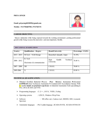
- 1. PRIYA SINGH Email: priyasingh020890@gmail.com Mobile: +91-9784687501, 9713765174 CAREER OBJECTIVE: Sincere dedication while being exposed towards the working environment ,seeking professional growth while being resourceful, innovative and most important, flexible. TECHNICAL QUALIFICATION: Obtained Certified Industrial Process Plant Robotics Automation Professional (CIPPRAP) from Technocrat Automation Pvt Limited (IAO Accredited), Chennai. With 2 months hands on practical experience in Industrial Automation Tools specializing in PLC, DCS, SCADA and VFD. Programming languages : C ,C++ , JAVA, VHDL ,Verilog Operating systems : LINUX , Windows 98/xp/Vista Software : MS office suit , Cadence tool , MODEL SIM , Leonardo Spectrum Automation languages : PLC Ladder language , SCADA IN FIX, SCADA INTOUCH Year(s) Qualification – Degree Board/University Percentage / CGPA 2013 - 2015 M.Tech – VLSI Design Banasthali vidyapith, Jaipur 76.70% 2008 - 2012 B. Tech Electronics & communication Rajiv Gandhi Technical University 76.40 % 2007 - 2008 XII C.B.S.E. 70.00 % 2005-2006 X C.B.S.E. 85.00 % EDUCATIONAL QUALIFICATIONS
- 2. TECHNICAL SKILLS: PLC (Programmable Logic Controllers) & DCS (Distributed Control System) - Programming languages such as LD(Ladder Diagram) & FBD (Functional Block Diagram) Hands on Practical exposure in brands as Siemens, AB (Allen Bradley), ABB (Asea Brown Boveri), Honeywell, Schneider, GE-Fanuc, Keyence, Omron, Messung, Mitsubishi, and Delta SCADA (Supervisory Control & Data Acquisition) – Screen designing, PC & PLC interface, Data collection & storage HMI (Human Machine Interface) - Screen designing, PLC interface, DCS interface PAC (Programmable Automation Controller) – X, Y axis Robotic Control using Servo motors & drives VFD (Variable Frequency Drive) – Commissioning and Troubleshooting Pneumatics & Field Instruments ( Control Valve, Sensors, Level Transmitters, Flow Transmitters, Temperature Transmitters, Pressure Switches) Interfacing between PLC & GSM modem to communicate with mobile device Knowledge in Panel wiring Knowledge in PID(Proportional Integral Derivative) 1 year of experience on ASIC layout and designing ,Worked with BARC Mumbai Versed with application like DRC, DFM , LVS and front end designing of chips.PRACTICALLY WORKED over CADENCE TOOLS in 28 um technology. Excellent exposure in chip designing and manufacturing. Qualified GATE with 90.4 percentile Troubleshooting – PLC & DCS programming - Control Panel (Power wiring & Control wiring) ACADEMIC PROJECT: One year Internship Program (M.Tech 2nd year) Duration: July 2014-April 2015 Company: “ BARC, Mumbai, Project Title: Design of 4 Channel Pulse Processing ASIC Description: The aim was to Design the Channel for detecting high energy physics particle and converting it to voltage signal for its further study. Design of on chip high voltage generator. M.Tech (1st year) Duration: July 2013-July 2014 Company: “In house project, Project Title: “VHDL implementation of DSDV Adhoc Routing Protocol.” Description: Had coded for the control unit of DSDV routing protocol to minimize the operating time. which is much reduced than its MATLAB counterpart. Summer Training Program (B.E 4th year) Company : MindsteinTech, Banglore Project Title: “VLSI Design” Description: ASIC Design using High Level Language “VHDL” B.E (major): Wireless IR detector in the high range. B.E(minor): Bidirectional Visitors counter
- 3. ACHIEVEMENTS / CO-CURRICULAR ACTIVITIES / EXTRA CURRICULAR ACTIVITIES: Published 3 international journals paper and one international conference paper. Had actively participated in IMPACT 2014 Conference in VIT Jaipur. Had done Robotics workshop at graduate level. Attended the HCL training Programs for Languages and Databases at graduate level. Had done the Cadence workshop in ASIC designing at post graduate level. Actively participated in Mayuk 2014 cultural fest at post graduate level. INPLANT TRAINING / WORK EXPERIENCE Company: Sine international institute of technology , Jaipur Duration : 1.6 years Designation: Assistant Professor Description: To tackle semester subjects and labs of EDC,VHDL,VLSI analog communication To manage college Co-Curricular activities Company:Bhabha Atomic Research Centre, Mumbai. Duration: July 2014-April 2015 Designation: Project Trainee Description: To perform Frontend and Backend Design of ASIC which includes schematic entry Circuit designing, Layout designing with DRC,LVS,DFM Verification and testing PERSONAL PROFILE: Father’s Name : Rajendra Kumar Singh Date of Birth : 02 August 1990 Gender : Female : Language Known : English, Hindi Address : I/9 Panchsheel Nagar , Gwarighat Road , Jabalpur, M.P – 482001 INDIA DECLARATION: I hereby declare that the above particulars furnished by me are true to the best of my knowledge and belief. Date: Place: (Name)