2. 1558 BRIEF REPORTS 54
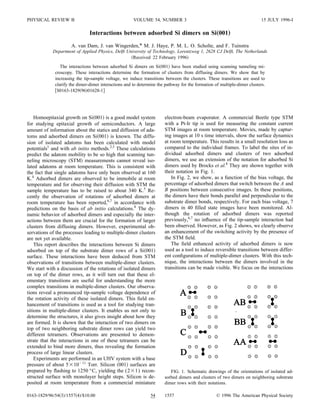
FIG. 2. Percentage of dimers that have rotated between consecu-
tive images as a function of the tip-sample voltage.
between dimers adsorbed on neighboring substrate dimer
rows. These are relevant upon annealing of a room tempera- FIG. 4. Filled a and empty b state image of a twin note that
ture grown submonolayer, as in that case adsorbed dimers a second twin is formed between the capturing of both images . The
will diffuse mainly along the substrate dimer rows.5,9 If two inset in b shows a schematic drawing of a twin horizontal gray
dimers adsorbed on neighboring rows happen to arrive next lines indicate new substrate dimer bonds . Interactions between
to each other, dimer-dimer interactions can cause the forma- three neighboring B dimers c,d ; the dimer in the middle is indi-
tion of a cluster. The formation of clusters from diffusing cated with an arrow. Tunneling conditions: 0.4 nA, 1.3 V a ; 0.4
dimers cannot be observed directly at room temperature, be- nA, 1.0 V b ; 0.4 nA, 1.5 V c,d .
cause then dimer diffusion is negligible. However, by ob-
serving the field enhanced transitions at room temperature, 3 form an AB configuration see Fig. 3 c . In the case of
we can analyze the dimer-dimer interactions without raising completely isolated dimers, we never observed such a hop-
the temperature. Using these observations, we discuss the ping of one position along the dimer row at room tempera-
structures resulting from the interactions in case of the three ture. The presence of dimer 2 probably lowered the barrier
possible starting configurations, viz. AB, BB, and AA, as for the hopping of dimer 3. Apparently dimers on neighbor-
shown in Fig. 1. ing rows attract each other in order to form lines perpendicu-
The images in Fig. 3, which are taken from a movie, show lar to the substrate dimer rows. The appearance of the ad-
the formation of structures as a result of dimer-dimer inter- sorbed dimers in the AB configuration is not noticeably
actions. In Fig. 3 a , all three dimers 1,2,3 are positioned different from that of the corresponding isolated dimers.
on top of the substrate dimer rows. Between Figs. 3 a and Thus, the dimer-dimer interaction in the AB configuration
3 b dimer 3 rotates, just as an isolated dimer. Then dimer 3 does not lead to a visible reconfiguration of the structure. As
hops one position along the dimer row, so that dimers 2 and Fig. 3 d shows, a subsequent rotation of dimer 2 results in a
modified BB configuration. The modification of the structure
is obvious from the much fainter appearance of the dimers
2,3 of the BB configuration, as compared to the appearance
of an isolated dimer e.g., dimer 1 . Hence, the interaction
leads to a different structure: a tetramer, which we call a
‘‘twin.’’ Filled and empty state images of a twin are shown
in Figs. 4 a and 4 b , respectively. Due to the interaction the
spacing between the dimers is smaller, which is most clearly
observed in the empty state image Fig. 4 b . The smaller
spacing can be understood if one assumes that the substrate
dimer bonds below the twin dimers are broken, and that new
dimer bonds are formed between the substrate atoms in be-
tween the twin dimers see the inset in Fig. 4 b . The break-
ing of the substrate dimer bonds presumably causes a de-
crease in height of the twin dimers. This can explain their
fainter appearance, although changes in the electronic struc-
ture should also be taken into account.
It is not possible to extend the twin to a triplet with the
same type of interaction. In the two images in Figs. 4 c and
4 d , which are taken from another movie, the middle of the
three B dimers forms a faintly visible twin with either of its
neighbors, but not with both of them simultaneously. The
remaining bright B dimer appears to be identical to an iso-
FIG. 3. Formation of a twin from two individual dimers a–d . lated one. A repeated switching between these two configu-
Tunneling conditions: 1.1 nA, 1.2 V. rations was observed.
3. 54 BRIEF REPORTS 1559
FIG. 5. The formation of a cross b from a twin a . Filled c
and empty d state images of a cross indicated with an arrow and
an isolated C dimer inside the circle with a schematic drawing of
the cross structure inset . Tunneling conditions: 1.1 nA, 1.9 V
a,b ; 1.0 nA, 1.5 V c ; 1.0 nA, 1.3 V d .
The third possible two-dimer structure, the AA configura- FIG. 6. Cross structure with B dimer filled a and empty c
tion, leads to a strong reconfiguration of the bonds. The tran- state transformed to an extended diluted dimer row filled b and
sition from a twin to this structure is shown in Figs. 5 a and empty d state . Schematic drawings of the initial e and final state
5 b . The same structure has been indicated with an arrow in f with the intermediate state g . Tunneling conditions: 0.4 nA,
the filled and empty state images in Figs. 5 c and 5 d . 1.6 V a,b ; 0.4 nA, 1.6 V c,d .
Because the substrate dimer rows seem to bend towards the
bright spot in between them, we call it a ‘‘cross’’ structure. It that the shortest diluted dimer row, formed from two dimers,
can easily be misinterpreted as a two-atom instead of a four- is stable. We now deduce the pathway for the extension of
atom structure, because the white spot in between the sub- diluted dimer rows with adsorbed dimers. Figures 6 a and
strate dimer rows is very similar to the appearance of a dimer 6 b show the extension of the shortest diluted dimer row
on top of the substrate dimer rows. Apart from the rotation of with two atoms from a B dimer. Empty state images of the
both dimers, the transition in Figs. 5 a and 5 b also in- same transition are shown in Figs. 6 c and 6 d . The two
volves a reconfiguration of the dimer bonds. The single corresponding structures are drawn schematically in Figs.
bright dot in the filled state image indicates that a dimer bond 6 e and 6 f . We have analyzed the time dependent height
is formed between the two atoms in the middle. The two signal measured with the STM tip positioned right above the
remaining adatoms at the ends are not visible in the filled end of a diluted dimer row. This height signal switches be-
state image Fig. 5 c , while they are in the empty state Fig. tween two levels, the lower level corresponding to the struc-
5 d . This illustrates the importance of using both the filled ture in Fig. 6 b and the other one to a structure with a dimer
and empty state images. The structural model, which is on top of the substrate dimer row. As we have observed two
drawn schematically in the inset in Fig. 5 d , is confirmed by significantly different lifetimes for the higher level, we con-
ab initio calculations.10 The cross structure has a lower en- clude that the transition should involve an intermediate state.
ergy than two single dimers in the AA configuration, as no Because of the short lifetime of this intermediate state, STM
stable structures of the latter have been observed. It should movies only indicate its existence by bright speckles ob-
be stressed that the adatoms at both ends result from a re- served at the end of the extended diluted dimer row. The
configuration of the dimer bonds of an AA structure and do most likely pathway for the extension of the diluted dimer
not originate from the sticking of single adatoms to a C row is the rotation of the B dimer, thus forming the interme-
dimer. The number of cross structures can be increased by diate state in Fig. 6 g , followed by a reconfiguration of the
annealing the surface. This easily leads to the wrong conclu- bonds. This model is consistent with the fact that both the
sion that the number of isolated dimers in between the dimer short and the long lifetime high level have the same height,
rows increases. However, using both filled and empty states, because the apparent height of A and B dimers is also iden-
the isolated C dimer,11 indicated by the circles in Figs. 5 c tical.
and 5 d is easily distinguished from the cross structure. A point of discussion regarding the observed pathways is
Extended forms of the cross structure have previously their validity in the absence of the electric field. For isolated
been reported and were denoted as diluted dimer rows.7,12 dimers, however, the observed field effect is similar to the
The experimental observation of the cross structure shows effect of raising the temperature, as predicted using ab initio
4. 1560 BRIEF REPORTS 54
calculations.8,10 As the transitions observed in clusters also figuration show hardly any interaction. However, dimers in
involve these basic transitions, it can be expected that they an AA or BB configuration interact, resulting in the forma-
are also enhanced upon raising the temperature. Furthermore, tion of a cross and a twin structure, respectively. The previ-
the structures resulting from transitions observed by scan- ously undescribed twin structure is difficult to recognize be-
ning at high bias voltages are also observed on surfaces cause of its faint appearance. The interaction forming a twin
scanned for the first time at low bias voltages e.g., 1.1 V . cannot bind more than two dimers to form larger clusters.
This shows that the specific bond reconfigurations also occur The cross structure is a short form of the so-called diluted
under zero-field conditions. Thus, the high bias voltages only dimer rows. It requires special attention because this starting
enhance the activity of individual adsorbed dimers and point for the growth of a long diluted dimer row is easily
dimers in clusters without creating new structures. The rela- misinterpreted as a single dimer in between the substrate
tive frequencies of occurrence of certain configurations, dimer rows. The corresponding dimer-dimer interaction can
however, have to be interpreted with some care. be used to bind more dimers in the linear structure. The
We conclude that the STM field strongly influences the pathway for the extension of this structure from diffusing
transition activity of dimers adsorbed on top of the substrate dimers has also been deduced.
dimer rows. The observation of similar field enhanced tran-
sitions in multiple-dimer clusters is demonstrated to be a The authors would like to thank C.D. Laman, R.F. Staak-
powerful tool for analyzing dimer-dimer interactions. The man, and H. Vogelaar for their technical support in building
interaction depends on the relative orientation of the dimers the UHV-STM setup. Furthermore, we thank G. Brocks for
on neighboring dimer rows. Nonparallel dimers (AB con- showing us his results prior to publication.
* 6
Author to whom all correspondence should be addressed. Z. Zhang, F. Wu, H.J.W. Zandvliet, B. Poelsema, H. Metiu, and
1
Y.-T. Lu, Z. Zhang, and H. Metiu, Surf. Sci. 257, 199 1991 . M.G. Lagally, Phys. Rev. Lett. 74, 3644 1995 .
2 7
G. Brocks, P.J. Kelly, and R. Car, Phys. Rev. Lett. 66, 1729 P.J. Bedrossian, Phys. Rev. Lett. 74, 3648 1995 .
1991 . 8
G. Brocks, P.J. Kelly, and R. Car, Surf. Sci. 269/270, 860 1992 .
3 9
Q.-M Zhang, C. Roland, P. Boguslawski, and J. Bernholc, Phys. B.S. Swartzentruber, Phys. Rev. Lett. 76, 459 1996 .
Rev. Lett. 75, 101 1995 . 10
G. Brocks and P.J. Kelly, Phys. Rev. Lett. 76, 2362 1996 .
4
R.A. Wolkow, Phys. Rev. Lett. 74, 4448 1995 . 11
J. van Wingerden, A. van Dam, M.J. Haye, P.M.L.O. Scholte, and
5
D. Dijkkamp, E.J. van Loenen, and H.B. Elswijk, in Ordering at F. Tuinstra unpublished .
Surfaces and Interfaces, edited by A. Yoshimori, T. Shinjo, and 12
Y.-W. Mo, R. Kariotis, B.S. Swartzentruber, M.B. Webb, and
H. Watanabe, Springer Series in Materials Science Vol. 17 M.G. Lagally, J. Vac. Sci. Technol. A 8, 201 1990 .
Springer, Berlin, 1992 .