

Empfohlen
Weitere ähnliche Inhalte
Was ist angesagt?
Was ist angesagt? (20)
Ähnlich wie Composites
Ähnlich wie Composites (20)
Mehr von NEERAJ PARMAR
Kürzlich hochgeladen
Kürzlich hochgeladen (20)
Composites
- 3. • What makes a material a composite? • Composite materials are formed by combining two or more materials that have quite different properties. • The different materials work together to give the composite unique properties, but within the composite you can easily tell the different materials apart – they do not dissolve or blend into each other.
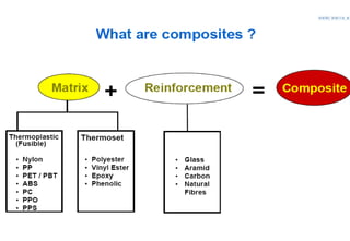
- 6. • Making a composite • Most composites are made up of just two materials. One material (the matrix or binder) surrounds and binds together a cluster of fibres or fragments of a much stronger material (the reinforcement). • In the case of mud bricks, the two roles are taken by the mud and the straw; in concrete, by the cement and the aggregate; in a piece of wood, by the cellulose and the lignin. In fibreglass, the reinforcement is provided by fine threads or fibres of glass, often woven into a sort of cloth, and the matrix is a plastic.
- 10. • The greatest advantage of composite materials is strength and stiffness combined with lightness. By choosing an appropriate combination of reinforcement and matrix material, manufacturers can produce properties that exactly fit the requirements for a particular structure for a particular purpose. • Modern aviation, both military and civil, is a prime example. It would be much less efficient without composites. In fact, the demands made by that industry for materials that are both light and strong has been the main force driving the development of composites. It is common now to find wing and tail sections, propellers and rotor blades made from advanced composites, along with much of the internal structure and fittings. The airframes of some smaller aircraft are made entirely from composites, as are the wing, tail and body panels of large commercial aircraft. • In thinking about planes, it is worth remembering that composites are less likely than metals (such as aluminium) to break up completely under stress. A small crack in a piece of metal can spread very rapidly with very serious consequences (especially in the case of aircraft). The fibres in a composite act to block the widening of any small crack and to share the stress around.
- 11. • The right composites also stand up well to heat and corrosion. This makes them ideal for use in products that are exposed to extreme environments such as boats, chemical-handling equipment and spacecraft. In general, composite materials are very durable. • Another advantage of composite materials is that they provide design flexibility. Composites can be moulded into complex shapes – a great asset when producing something like a surfboard or a boat hull. • The downside of composites is usually the cost. Although manufacturing processes are often more efficient when composites are used, the raw materials are expensive. Composites will never totally replace traditional materials like steel, but in many cases they are just what we need. And no doubt new uses will be found as the technology evolves. We haven’t yet seen all that composites can do.
- 29. Putting it together – the science and technology of composite materials •Australia, like all advanced countries, is taking a big interest in composite materials, which many people see as 'the materials of the future'. The main concern is to get the costs down, so that composites can be used in products and applications which at present don’t justify the cost. At the same time researchers want to improve the performance of the composites, such as making them more resistant to impact. •One new technique involves 'textile composites'. Instead of the reinforcing fibres being put in place individually, which is slow and costly, they can be knitted or woven together to make a sort of cloth. This can even be three- dimensional rather than flat. The spaces between and around the textile fibres are then filled with the matrix material (such as a resin) to make the product.
- 30. • This process can quite easily be done by machines rather than by hand, making it faster and cheaper. Connecting all the fibres together also means that the composite is less likely to be damaged when struck. • With the costs coming down, other uses for composites are beginning to look attractive. Making the hulls and superstructures of boats from composites takes advantage of their resistance to corrosion. The Australian Navy’s new minehunters have composite hulls, since the magnetic effect of a steel hull would interfere with mine detection. • Also in the pipeline are carriages for trains, trams and other 'people movers', made from composites rather than steel or aluminium. Here the appeal is the lightness of the composites, as the vehicles then use less energy. And we are going to see more and more composites in cars for the same reason.
- 31. INTRODUCTION TO NANOMATERIAL • Nanomaterials is the study of how materials behave when their dimensions are reduced to the nanoscale. It can also refer to the materials themselves that are used in nanotechnology. • A unique aspect of nanotechnology is the vastly increased ratio of surface area to volume present in many nanoscale materials which opens new possibilities in surface-based science, such as catalysis
- 32. • A number of physical phenomena become noticeably pronounced as the size of the system decreases. • These include statistical mechanical effects, as well as quantum mechanical effects, for example the “quantum size effect” where the electronic properties of solids are altered with great reductions in particle size. • This effect does not come into play by going from macro to micro dimensions. However, it becomes dominant when the nanometer size range is reached. • Additionally, a number of physical properties change when compared to macroscopic systems. • One example is the increase in surface area to volume of materials. Novel mechanical properties of nanomaterials is the subject of nanomechanics research. • Their catalytic activity reveals novel properties in the interaction with biomaterials.
- 33. What is the effect of nonmaterial? • Materials reduced to the nanoscale can suddenly show very different properties compared to what they exhibit on a macroscale, enabling unique applications. • For instance, opaque substances become transparent (copper); • inert materials become catalysts (platinum); • stable materials turn combustible (aluminum); • solids turn into liquids at room temperature (gold); • insulators become conductors (silicon). • Materials such as gold, which is chemically inert at normal scales, can serve as a potent chemical catalyst at nanoscales. • Much of the fascination with nanotechnology stems from these unique quantum and surface phenomena that matter exhibits at the nanoscale.
- 34. • Nanosize powder particles (a few nanometres in diameter, also called nanoparticles) are potentially important in ceramics, powder metallurgy, the achievement of uniform nanoporosity and similar applications. • The strong tendency of small particles to form clumps ("agglomerates") is a serious technological problem that impedes such applications.
- 35. Materials used in nanotechnology • Fullerenes and carbon forms • Nanoparticles and Colloids
- 36. Fullerenes and carbon forms • Allotropes of carbon • Aggregated diamond nanorods • Buckypaper • Carbon nanofoam • Carbon nanotube • Nanoknot* • Fullerene chemistry • Bingel reaction • Endohedral hydrogen fullerene • Prato reaction • Fullerenes in popular culture • Endohedral fullerenes • Fullerite • Graphene • Potential applications of carbon nanotubes • Timeline of carbon nanotubes
- 37. Nanoparticles and Colloids • Colloid • Diamondoids • Nanocomposite • Nanocrystal • Nanostructure – Nanocages – Nanocomposite – Nanofabrics – Nanofiber – Nanofoam – Nanoknot – Nanomesh – Nanopillar – Nanopin film – Nanoring – Nanorod – Nanoshell – Nanotube – Quantum heterostructure – Sculptured thin film • Quantum dot
- 38. Fullerenes • The fullerenes are a class of allotropes of carbon which conceptually are graphene sheets rolled into tubes or spheres. • These include the carbon nanotubes which are of interest due to both their mechanical strength and their electrical properties. • For the past decade, the chemical and physical properties of fullerenes have been a hot topic in the field of research and development, and are likely to continue to be for a long time. • In April 2003, fullerenes were under study for potential medicinal use: binding specific antibiotics to the structure to target resistant bacteria and even target certain cancer cells such as melanoma.
- 39. • The October 2005 issue of Chemistry and Biology contains an article describing the use of fullerenes as light-activated antimicrobial agents. • In the field of nanotechnology, heat resistance and superconductivity are some of the more heavily studied properties. • A common method used to produce fullerenes is to send a large current between two nearby graphite electrodes in an inert atmosphere. The resulting carbon plasma arc between the electrodes cools into sooty residue from which many fullerenes can be isolated. • There are many calculations that have been done using ab-initio Quantum Methods applied to fullerenes. By DFT and TDDFT methods one can obtain IR, Raman and UV spectra. Results of such calculations can be compared with experimental results.
- 40. Nanoparticles • Nanoparticles or nanocrystals made of metals, semiconductors, or oxides are of interest for their electrical, optical, and chemical properties. Nanoparticles have been used as quantum dots and as chemical catalysts. • Nanoparticles are of great scientific interest as they are effectively a bridge between bulk materials and atomic or molecular structures. A bulk material should have constant physical properties regardless of its size, but at the nano- scale this is often not the case. Size-dependent properties are observed such as quantum confinement in semiconductor particles, surface plasmon resonance in some metal particles and superparamagnetism in magnetic materials.
- 41. Nanopartical continue... • Nanoparticles exhibit a number of special properties relative to bulk material. For example, the bending of bulk copper (wire, ribbon, etc.) occurs with movement of copper atoms/clusters at about the 50 nm scale. Copper nanoparticles smaller than 50 nm are considered super hard materials that do not exhibit the same malleability and ductility as bulk copper. • The change in properties is not always desirable. Ferroelectric materials smaller than 10 nm can switch their magnetisation direction using room temperature thermal energy, thus making them useless for memory storage.
- 42. • Suspensions of nanoparticles are possible because the interaction of the particle surface with the solvent is strong enough to overcome differences in density, which usually result in a material either sinking or floating in a liquid. Nanoparticles often have unexpected visible properties because they are small enough to confine their electrons and produce quantum effects. For example gold nanoparticles appear deep red to black in solution. • Nanoparticles have a very high surface area to volume ratio. This provides a tremendous driving force for diffusion, especially at elevated temperatures. Sintering can take place at lower temperatures, over shorter time scales than for larger particles. This theoretically does not affect the density of the final product, though flow difficulties and the tendency of nanoparticles to agglomerate complicates matters. The surface effects of nanoparticles also reduces the incipient melting temperature.
- 43. Potential applications of carbon nanotubes • Structural • clothes: waterproof tear-resistant • combat jackets: MIT is working on combat jackets that use carbon nanotubes as ultrastrong fibers and to monitor the condition of the wearer. [1] • concrete: In concrete, they increase the tensile strength, and halt crack propagation. • polyethylene: Researchers have found that adding them to polyethylene increases the polymer's elastic modulus by 30%. • sports equipment: Stronger and lighter tennis rackets, bike parts, golf balls, golf clubs, golf shaft and baseball bats. • space elevator: This will be possible only if tensile strengths of more than about 70 GPa can be achieved. Monoatomic oxygen in the Earth's upper atmosphere would erode carbon nanotubes at some altitudes, so a space elevator constructed of nanotubes would need to be protected (by some kind of coating). Carbon nanotubes in other applications would generally not need such surface protection. • ultrahigh-speed flywheels: The high strength/weight ratio enables very high speeds to be achieved. • Bridges: For instance in suspension bridges (where they will be able to replace steel), or bridges built as a "horizontal space elevator".
- 44. Electromagnetic • artificial muscles Electroactive Polymers or EAPs are polymers whose shape is modified when a voltage is applied to them. They can be used as actuators or sensors. As actuators, they are characterized by the fact that they can undergo a large amount of deformation while sustaining large forces. Due to the similarities with biological tissues in terms of achievable stress and force, they are often called artificial muscles, and have the potential for application in the field of robotics, where large linear movement is often needed. • buckypaper - a thin sheet made from nanotubes that are 250 times stronger than steel and 10 times lighter that could be used as a heat sink for chipboards, a backlight for LCD screens or as a faraday cage to protect electrical devices/aeroplanes. • chemical nanowires: Carbon nanotubes additionally can also be used to produce nanowires of other chemicals, such as gold or zinc oxide. These nanowires in turn can be used to cast nanotubes of other chemicals, such as gallium nitride. These can have very different properties from CNTs - for example, gallium nitride nanotubes are hydrophilic, while CNTs are hydrophobic, giving them possible uses in organic chemistry that CNTs could not be used for.
- 45. • computer circuits: A nanotube formed by joining nanotubes of two different diameters end to end can act as a diode, suggesting the possibility of constructing electronic computer circuits entirely out of nanotubes. Because of their good thermal properties, CNTs can also be used to dissipate heat from tiny computer chips. The longest electricity conducting circuit is a fraction of an inch long. (Source: June 2006 National Geographic). • conductive films: A 2005 paper in Science notes that drawing transparent high strength swathes of SWNT is a functional production technique (Zhang et al., vol. 309, p. 1215). Additionally, Eikos Inc of Franklin, Massachusetts and Unidym Inc. [2] of Silicon Valley, California are developing transparent, electrically conductive films of carbon nanotubes to replace indium tin oxide (ITO) in LCDs, touch screens, and photovoltaic devices. Carbon nanotube films are substantially more mechanically robust than ITO films, making them ideal for high reliability touch screens and flexible displays. Nanotube films show promise for use in displays for computers, cell phones, PDAs, and ATMs.
- 46. • electric motor brushes: Conductive carbon nanotubes have been used for several years in brushes for commercial electric motors. They replace traditional carbon black, which is mostly impure spherical carbon fullerenes. The nanotubes improve electrical and thermal conductivity because they stretch through the plastic matrix of the brush. This permits the carbon filler to be reduced from 30% down to 3.6%, so that more matrix is present in the brush. Nanotube composite motor brushes are better-lubricated (from the matrix), cooler-running (both from better lubrication and superior thermal conductivity), less brittle (more matrix, and fiber reinforcement), stronger and more accurately moldable (more matrix). Since brushes are a critical failure point in electric motors, and also don't need much material, they became economical before almost any other application. • light bulb filament: alternative to in incandescent lamps. • magnets: MWNTs coated with magnetite • optical ignition: A layer of 29% iron enriched SWNT is placed on top of a layer of explosive material such as PETN, and can be ignited with a regular camera flash.
- 47. • solar cells: GE's carbon nanotube diode has a photovoltaic effect. Nanotubes can replace ITO in some solar cells to act as a transparent conductive film in solar cells to allow light to pass to the active layers and generate photocurrent. • superconductor: Nanotubes have been shown to be superconducting at low temperatures. • ultracapacitors: MIT is researching the use of nanotubes bound to the charge plates of capacitors in order to dramatically increase the surface area and therefore energy storage ability.[3] • displays: One use for nanotubes that has already been developed is as extremely fine electron guns, which could be used as miniature cathode ray tubes in thin high-brightness low-energy low-weight displays. This type of display would consist of a group of many tiny CRTs, each providing the electrons to hit the phosphor of one pixel, instead of having one giant CRT whose electrons are aimed using electric and magnetic fields. These displays are known as field emission displays (FEDs). • transistor: developed at Delft, IBM, and NEC.
- 48. Chemical • air pollution filter: Future applications of nanotube membranes include filtering carbon dioxide from power plant emissions.[4] • biotech container: Nanotubes can be opened and filled with materials such as biological molecules, raising the possibility of applications in biotechnology. • hydrogen storage: Research is currently being undertaken into the potential use of carbon nanotubes for hydrogen storage. They have the potential to store between 4.2 and 65% hydrogen by weight. This is an important area of research, since if they can be mass produced economically there is potential to contain the same quantity of energy as a 50l gasoline tank in 13.2l of nanotubes. See also, Hydrogen Economy.[5] • water filter: Recently nanotube membranes have been developed for use in filtration. This technique can purportedly reduce desalination costs by 75%. The tubes are so thin that small particles (like water molecules) can pass through them, while larger particles (such as the chloride ions in salt) are blocked.
- 49. Mechanical • oscillator: fastest known oscillators (> 50 GHz). • nanotube membrane: Liquid flows up to five orders of magnitude faster than predicted by classical fluid dynamics. • slick surface: slicker than Teflon and waterproof.
- 50. In electrical circuits • Carbon nanotubes have many properties—from their unique dimensions to an unusual current conduction mechanism— that make them ideal components of electrical circuits. Currently, there is no reliable way to arrange carbon nanotubes into a circuit. • The major hurdles that must be jumped for carbon nanotubes to find prominent places in circuits relate to fabrication difficulties. The production of electrical circuits with carbon nanotubes are very different from the traditional IC fabrication process. The IC fabrication process is somewhat like sculpture - films are deposited onto a wafer and pattern-etched away. Because carbon nanotubes are fundamentally different from films, carbon nanotube circuits can so far not be mass produced.
- 51. Some other important applications • Metallic and semiconducting nanotubes • Carbon Nanotube Interconnects • Carbon Nanotube Transistors • Challenges in Electronic Design and Design Automation • As fiber and film
- 52. MAGNETIC MATERIAL • When a material is placed within a magnetic field, the magnetic forces of the material's electrons will be affected. This effect is known as Faraday's Law of Magnetic Induction. However, materials can react quite differently to the presence of an external magnetic field. This reaction is dependent on a number of factors, such as the atomic and molecular structure of the material, and the net magnetic field associated with the atoms. The magnetic moments associated with atoms have three origins. These are the electron orbital motion, the change in orbital motion caused by an external magnetic field, and the spin of the electrons.
- 53. • In most atoms, electrons occur in pairs. Electrons in a pair spin in opposite directions. So, when electrons are paired together, their opposite spins cause their magnetic fields to cancel each other. Therefore, no net magnetic field exists. Alternately, materials with some unpaired electrons will have a net magnetic field and will react more to an external field. Most materials can be classified as diamagnetic, paramagnetic or .ferromagnetic.
- 54. Applications • Magnetic materials encompass a wide variety of materials, which are used in a diverse range of applications. • Magnetic materials are utilized in the creation and distribution of electricity, and, in most cases, in the appliances that use that electricity. • They are used for the storage of data on audio and video tape as well as on computer disks. • In the world of medicine, they are used in body scanners as well as a range of applications where they are attached to or implanted into the body. • The home entertainment market relies on magnetic materials in applications such as PCs, CD players, televisions, games consoles and loud speakers. • It is difficult to imagine a world without magnetic materials and they are becoming more important in the development of modern society. • The need for efficient generation and use of electricity is dependent on improved magnetic materials and designs. Non-polluting electric vehicles will rely on efficient motors utilising advanced magnetic materials. • The telecommunications industry is always striving for faster data transmission and miniaturisation of devices, both of which require development of improved magnetic materials. • Metallic glasses are excellent ferromagnets. Possessing high magnetic moments, very high permeability and zero magnostriction. They are hard and corrosion resistant therefore they are suitable for use as the magnetic head recorder. They can be easily magnetize hence also find application in magnetic shielding , motors, transformers etc.
- 55. Classification • Magnetic materials are classified in terms of their magnetic properties and their uses. • If a material is easily magnetised and demagnetised then it is referred to as a soft magnetic material, whereas if it is difficult to demagnetise then it is referred to as a hard (or permanent) magnetic material. • Materials in between hard and soft are almost exclusively used as recording media and have no other general term to describe them. • Other classifications for types of magnetic materials are subsets of soft or hard materials, such as magnetostrictive and magnetoresistive materials.
- 56. All materials can be classified in terms of their magnetic behaviour falling into one of five categories depending on their bulk magnetic susceptibility. The two most common types of magnetism are diamagnetism and paramagnetism, which account for the magnetic properties of most of the periodic table of elements at room temperature (see figure). These elements are usually referred to as non- magnetic, whereas those which are referred to as magnetic are actually classified as ferromagnetic. The only other type of magnetism observed in pure elements at room temperature is antiferromagnetism. Finally, magnetic materials can also be classified as ferrimagnetic although this is not observed in any pure element but can only be found in compounds, such as the mixed oxides, known as ferrites, from which ferrimagnetism derives its name. The value of magnetic susceptible falls into a particular range for each type of material and this is shown in table 2 with some examples.
- 57. Type of magnetic Susceptibility Atomic / Magnetic Behaviour Example / Susceptibility material/Magnetism X=rel. permeabitiy-1 Rel. per.=abs.per./per. Atoms have no magnetic Au -2.74x10⁻⁶ Diamagnetic Of free space. moment. Cu -0.77x10⁻⁶ Abs.per.=B/H Magnetic lines of force Si -0.3x10⁻⁵ materials Small & negative. are repelled by Al2O3 -0.5x10⁻⁵ Diamagnetism i.e., they cannot be diamagnetic solid. -2.1x10⁻⁵ diamond made from magnets Atoms have randomly β-Sn paramagnetic oriented magnetic Pt 0.19x10⁻⁶ 21.04x10⁻⁶ materials Small & positive. moments. Mn Fe2O3 66.10x10⁻⁶ They are week magnet. Magnetic line of forces 1.40x10⁻³ Feebly attract by Fecl2 Paramagnetism 3.7x10⁻³ paramagnetic solid Large & positive, Atoms have parallel ferromagnetic function of applied field, aligned magnetic Picture 41 microstructure moments. materials dependent. Magnetic line of forces Fe ~100,000 They are very good Strongly attract by Ferromagnetism magnetic material. ferromagnetic solid. Table 2: Summary of different types of magnetic behaviour.
- 58. • Diamagnetic metals have a very weak and negative susceptibility to magnetic fields. Diamagnetic materials are slightly repelled by a magnetic field and the material does not retain the magnetic properties when the external field is removed. Diamagnetic materials are solids with all paired electron resulting in no permanent net magnetic moment per atom. Diamagnetic properties arise from the realignment of the electron orbits under the influence of an external magnetic field. Most elements in the periodic table, including copper, silver, and gold, are diamagnetic.
- 59. • Paramagnetic metals have a small and positive susceptibility to magnetic fields. These materials are slightly attracted by a magnetic field and the material does not retain the magnetic properties when the external field is removed. Paramagnetic properties are due to the presence of some unpaired electrons, and from the realignment of the electron orbits caused by the external magnetic field. Paramagnetic materials include magnesium, molybdenum, lithium, and tantalum.
- 60. • Ferromagnetic materials have a large and positive susceptibility to an external magnetic field. • They exhibit a strong attraction to magnetic fields and are able to retain their magnetic properties after the external field has been removed. • Ferromagnetic materials have some unpaired electrons so their atoms have a net magnetic moment. • They get their strong magnetic properties due to the presence of magnetic domains. • In these domains, large numbers of atom's moments (1012 to 1015) are aligned parallel so that the magnetic force within the domain is strong. When a ferromagnetic material is in the unmagnitized state, the domains are nearly randomly organized and the net magnetic field for the part as a whole is zero. When a magnetizing force is applied, the domains become aligned to produce a strong magnetic field within the part. Iron, nickel, and cobalt are examples of ferromagnetic materials. Components with these materials are commonly inspected using the magnetic particle method.
- 61. DIELECTRIC (INSULATORS) INTRODUCTION • A dielectric material is a substance that is a poor conductor of electricity, but an efficient supporter of electrostatic fields. If the flow of current between opposite electric charge poles is kept to a minimum while the electrostatic lines of flux are not impeded or interrupted, an electrostatic field can store energy. This property is useful in capacitors, especially at radio frequencies. Dielectric materials are also used in the construction of radio-frequency transmission lines.
- 62. Characteristics • They have the value of resistivity . (Electrical resistivity also known as specific electrical resistance) is a measure of how strongly a material opposes the flow of electric current. A low resistivity indicates a material that readily allows the movement of electrical charge. The SI unit of electrical resistivity is the ohm metre, ρ =RA/L). • Negative temperature coefficient of resistant (α). • Large insulation resistant. • They have very conductor to hear and electricity.
- 63. • In practice, most dielectric materials are solid. Examples include porcelain (ceramic), mica, glass, plastics, and the oxides of various metals. • Some liquids and gases can serve as good dielectric materials. • Dry air is an excellent dielectric, and is used in variable capacitors and some types of transmission lines. • Distilled water is a fair dielectric. A vacuum is an exceptionally efficient dielectric.
- 64. • An important property of a dielectric is its ability to support an electrostatic field while dissipating minimal energy in the form of heat. The lower the dielectric loss (the proportion of energy lost as heat), the more effective is a dielectric material. • Another consideration is the dielectric constant, the extent to which a substance concentrates the electrostatic lines of flux. • Substances with a low dielectric constant include a perfect vacuum, dry air, and most pure, dry gases such as helium and nitrogen. • Materials with moderate dielectric constants include ceramics, distilled water, paper, mica, polyethylene, and glass. Metal oxides, in general, have high dielectric constants.
- 65. Uses • In electrical Insulation. • They are used as insulators and capacitors. • Used in strain gauge and sonar devices. • Formvar is a suitable insulating material for low temp. applications. It is the trade mane of polyvinyl formal. • As a dielectric materials.
- 66. SEMICONDUCTOR(INSULATOR) Introduction • A semiconductor is a solid material that has electrical conductivity in between that of a conductor and that of an insulator; it can vary over that wide range either permanently or dynamically. • Semiconductors are tremendously important in technology. Semiconductor devices, electronic components made of semiconductor materials, are essential in modern electrical devices. • Examples range from computers to cellular phones to digital audio players. Silicon is used to create most semiconductors commercially, but dozens of other materials are used as well. • They have widely used for making solid state devices.
- 67. • Semiconductor is classified by two categories • Intrinsic-in which the elemental form of pure silica (Si) and Pure germanium (Ge) are intrinsic. In intrinsic form they are not useful. They are therefore doped by dopen to make extrinsic semiconductor.Extrinsic form are directly useful and are widely employed in manufacturing of solid state devises. • Extinsic- conduction in extrinsic occurs due to the presence of foreign impurities. An extrinsic semiconductor is a semiconductor that has been doped, that is, into which a doping agent has been introduced, giving it different electrical properties than the intrinsic (pure) semiconductor. • Doping involves adding dopant atoms to an intrinsic semiconductor, which changes the electron and hole carrier concentrations of the semiconductor at thermal equilibrium. • Dominant carrier concentrations in an extrinsic semiconductor classify it as either an n-type or p-type semiconductor. The electrical properties of extrinsic semiconductors make them essential components of many electronic devices.
- 68. n-type or p-type semiconductor • The phrase 'n-type' comes from the negative charge of the electron. In n-type semiconductors, electrons are the majority carriers and holes are the minority carriers. N-type semiconductors are created by doping an intrinsic semiconductor with donor impurities. In an n-type semiconductor, the Fermi energy level is greater than the that of the intrinsic semiconductor and lies closer to the conduction band than the valence band. • P-type semiconductors • Band structure of a p-type semiconductor. Dark circles in the conduction band are electrons and light circles in the valence band are holes. The image shows that the holes are the majority charge carrier.
- 69. N-type semiconductors • Extrinsic semiconductors with a larger electron concentration than hole concentration are known as n-type semiconductors. • The phrase 'n-type' comes from the negative charge of the electron. In n-type semiconductors, electrons are the majority carriers and holes are the minority carriers. • N-type semiconductors are created by doping an intrinsic semiconductor with donor impurities. • In an n-type semiconductor, the Fermi energy level is greater than the that of the intrinsic semiconductor and lies closer to the conduction band than the valence band
- 70. P-type semiconductors As opposed to n-type semiconductors, p-type semiconductors have a larger hole concentration than electron concentration. The phrase 'p-type' refers to the positive charge of the hole. In p- type semiconductors, holes are the majority carriers and electrons are the minority carriers. P-type semiconductors are created by doping an intrinsic semiconductor with acceptor impurities. P-type semiconductors have Fermi energy levels below the intrinsic Fermi energy level. The Fermi energy level lies closer to the valence band than the conduction band in a p-type semiconductor.
- 71. Utilization of extrinsic semiconductors • Extrinsic semiconductors are components of many common electrical devices. A semiconductor diode (devices that allow current flow in only one direction) consists of p-type and n-type semiconductors placed in junction with one another. Currently, most semiconductor diodes use doped silicon or germanium. • Transistors (devices that enable current switching) also make use of extrinsic semiconductors. Bipolar junction transistors (BJT) are one type of transistor. The most common BJTs are NPN and PNP type. NPN transistors have two layers of n-type semiconductors sandwiching a p-type semiconductor. PNP transistors have two layers of p- type semiconductors sandwiching an n-type semiconductor. • Field-effect transistors (FET) are another type of transistor implementing extrinsic semiconductors. As opposed to BJTs, they are unipolar and considered either N-channel or P-channel. FETs are broken into two families, junction gate FET (JFET) and insulated gate FET (IGFET). • Other devices implementing the extrinsic semiconductor: • Lasers • Solar cells • Photodetectors • Light-emitting diodes • Thyristors
- 72. SUPER CONDUCTOR -Introduction • Superconductors are those elements, compounds and alloys of metal and nonmetals which exhibits extra ordinary magnetic and electrical behavior at extremely low temperatures (near absolute zero). Such low temperatures are not practically favorable for wide application. • Superconductors, materials that have no resistance to the flow of electricity, are one of the last great frontiers of scientific discovery. Not only have the limits of superconductivity not yet been reached, but the theories that explain superconductor behavior seem to be constantly under review. • Superconductors have the ability to conduct electricity without the loss of energy.
- 73. Properties of super conductors • Super conducting materials exhibit the following extraordinary properties below their critical temperatures. • The magnetic flux density, B=0. • The relative permeability, μr=0. • The specific resistant, ρ=0. • The magnetic susceptibility, Χ=-1. • The power ( copper) loss, I2R=0.
- 74. Types • On the basis of working Temperature. i. low temp. super cond. ii. High temp. super cond. • On the basis of kind of material. i. metallic super conductor ii. Inter metallic compound superconductor iii. Ceramic super conductor. iv. Alloy super conductors • On the basis of kind of material. x. magnetic grade super conductor xi. Nonmagnetic grade super conductor
- 75. Superconductivity • Superconductivity is a phenomenon occurring in certain materials at extremely low temperatures, characterized by exactly zero electrical resistance and the exclusion of the interior magnetic field. • The electrical resistivity of a metallic conductor decreases gradually as the temperature is lowered. • However, in ordinary conductors such as copper and silver, impurities and other defects impose a lower limit. Even near absolute zero a real sample of copper shows a non-zero resistance. • The resistance of a superconductor, on the other hand, drops abruptly to zero when the material is cooled below its "critical temperature". An electrical current flowing in a loop of superconducting wire can persist indefinitely with no power source. Like ferromagnetism and atomic spectral lines, superconductivity is a quantum mechanical phenomenon. It cannot be understood simply as the idealization of " perfect conductivity" in classical physics.
- 76. Applications • Superconducting magnets are some of the most powerful electromagnets known. They are used in MRI and NMR machines and the beam-steering magnets used in particle accelerators. • They can also be used for magnetic separation, where weakly magnetic particles are extracted from a background of less or non-magnetic particles, as in the pigment industries. • Superconductors have also been used to make digital circuits (e.g. based on the Rapid Single Flux Quantum technology) and RF and microwave filters for mobile phone base stations. • Superconductors are used to build Josephson junctions which are the building blocks of SQUIDs (superconducting quantum interference devices), the most sensitive magnetometers known. Series of Josephson devices are used to define the SI volt. Depending on the particular mode of operation, a Josephson junction can be used as photon detector or as mixer. The large resistance change at the transition from the normal- to the superconducting state is used to build thermometers in cryogenic micro-calorimeter photon detectors. • Other early markets are arising where the relative efficiency, size and weight advantages of devices based on HTS outweigh the additional costs involved. • Promising future applications include high-performance transformers, power storage devices, electric power transmission, electric motors (e.g. for vehicle propulsion, as in vactrains or maglev trains), magnetic levitation devices, and Fault Current Limiters. However superconductivity is sensitive to moving magnetic fields so applications that use alternating current (e.g. transformers) will be more difficult to develop than those that rely upon direct current
- 77. Introduction-BIOMATERIALS • A biomaterial is any material, natural or man-made, that comprises whole or part of a living structure or biomedical device which performs, augments, or replaces a natural function. or • a nonviable material used in a medical device, intended to interact with biological systems or • A biomaterial is essentially a material that is used and adapted for a medical application
- 78. Biomaterial Applications • Biomaterials are used in: • Joint replacements • Bone plates • Bone cement • Artificial ligaments and tendons • Dental implants for tooth fixation • Blood vessel prostheses • Heart valves • Skin repair devices • Cochlear replacements • Contact lenses
- 79. • Ti alloy and carbon fiber-X-ray equipments • Liquid crystal polymer- optical fiber • Separation membranes- medical and biotechnology. • High temp. super conductor- medical imagine machine, magnetic resonance imaging (MRI)
- 80. Assignments Solutions 1. a. T = 3000ºF. Since the composition E is eutectoid, the carbon content is 0.83%. b. T = 2200ºF. At this temperature, austenite exists as a single-phase solid. c. T = 1333ºF. Two phases exist, ferrite and austenite. The percentages are determined by the lever rule: X ÷ (X+Y) = (Cy-C) ÷ (Cy-Cx). proeutectoid ferrite = (0.83 - 0.18) / (0.83 - 0.025) x 100 = 80.7% austenite = (0.18 - 0.025) / (0.83 - 0.025) x 100 = 19.3% d. T = 410ºF. A small amount of cementite will precipitate following the solubility line from 0.025% C at 1333ºF to 0.008% C at room temperature. The overall percentages of ferrite and cementite are: ferrite = (6.67 - 0.18) / (6.67 - 0.01) x 100 = 97.4 cementite = (0.18 - 0.01) / (6.67 - 0.01) x 100 = 2.6% 2. a. T = 3000ºF. At this temperature, the eutectic is all liquid. b. T = 1670ºF. Since there is a change of the solubility line, there will be a change in the austenite composition, that will transform to the eutectoid at 1333ºF. The overall austenite and cementite composition will be: austenite = (6.67 - 4.3) / (6.67 - 1.2) x 100 = 43.3% cementite = (4.3 - 1.2) / (6.67 - 1.2) x 100 = 56.7% c. T = 1333ºF. At this temperature the austenite has a eutectoid composition and will transform into pearlite. The compositions of proeutectoid cementite and austenite are: eutectoid austenite = (6.67 - 4.3) / (6.67 - 0.83) x 100 = 40.6% proeutectoid cementite = (4.3 - 0.83) / (6.67 - 0.83) x 100 = 59.4% The austenite has a eutectoid composition that is: eutectoid ferrite = (6.67 - 0.83) / (6.67 - 0.025) x 100 = 88% eutectoid cementite = (0.83 - 0.025) / (6.67 - 0.025) x 100 = 12% 3. Interpolate between alpha (0.02%C) and Fe3C (6.7%) at 1333ºF Carbide = (0.8 - 0.02) / (6.7 - 0.02) x 100 = 12g 4. Since pearlite originates from austenite of eutectoid composition, determine the amount of gamma just prior to the eutectoid reaction. From 870ºC - 780ºC : 100g austenite with 0.5% C From 780ºC - 727ºC : ferrite separates from austenite and the carbon content of the austenite increases to about 0.8% C At 727ºC (+) : proeutectoid ferrite: composition of ferrite = 0.02% C, amount of carbon = 38g Gamma that transforms to pearlite: compostion of austenite = 0.8% C. Amount of austenite = 62g. At 727ºC (-): Amount of pearlite = 62g
- 81. Home assignments • Point Z At the point represented by Z there are several questions to be considered: • What is the bulk composition of Point Z? Point Z has the same bulk composition as Point I, used above, as it lies on the same isopleth, but at a lower temperature. • What phases are present? Point Z lies in the field where two phases, B + L, are in equilibrium, therfore the two phases present have to be soild B and Liquid. • What are the proportions of the phases present? To determine the proportions of B + L at Z, carry out the following steps: – Draw a line through Z, parallel to the base of the diagram (This line is at a constant temperature and is an isotherm.) This line should extend only to the boundaries of the B + L field - Points X and Y. – Measure the three line segments - ZX, Zy and XY and ratio these lengths using the lever rule. • % B = ZX/XY * 100 = 38% B %L = ZY/XY * 100 = 62% L • What are the composition of the phases present? At Point Z if we were to examine the system we would see crystals of B in a glassy matrix (the Liquid) in equilibrium. The points X and Y assist us in determining the compostions of the two phases. As this is the simplest binary system possible, one which does not exhibit solid solution, all of the solid phases are of fixed composition. – Point Y lies on the right hand side of the binary system where we have 100% B and 0% A, therfore the solid represented by Y must have a composition of Pure B. The composition of the liquid in equilibrium with the Pure B is represented by X, on the liquidus surface. – To determine the composition of the Liquid at X, draw an isopleth down to the base of the diagram. – Now measure three line segments AX', BX' and AB, ratio these using the Lever Rule to get the composition of the liquid X, in terms of A and B, the two components which define the system. • %A = BX'/AB *100 = 40% A %B = AX'/AB*100 = 60% B