SlideShare ist ein Scribd-Unternehmen logo
1 von 14
Downloaden Sie, um offline zu lesen
International Journal of Trend in Scientific Research and Development (IJTSRD)
Volume 5 Issue 6, September-October 2021 Available Online: www.ijtsrd.com e-ISSN: 2456 – 6470
@ IJTSRD | Unique Paper ID – IJTSRD46406 | Volume – 5 | Issue – 6 | Sep-Oct 2021 Page 569
Technical Report: Comparative Analysis of Photodetectors for
Appropriate Usage in Optical Communication Applications
Obodoeze Fidelis Chukwujekwu1
, Obiokafor Ifeyinwa Nkemdilim2
1
Department of Computer Engineering Technology, Akanu Ibiam Federal Polytechnic Unwana, Nigeria
2
Department of Computer Science Technology, Anambra State Polytechnic, Mgbakwu, Nigeria
ABSTRACT
Photodetectors have found useful applications in various power and
electronic fields such as in microwave power amplifications and fibre
optic data communications. Different types of photodetectors,
especially the PIN photodiodes and Avalanche photodiodes, are the
most useful photodetectors in microwave and fibre optic
communications. In this paper, the authors x-rayed the different types
of photodetectors, the photodetectors’ principles, the fiber optic
communication architecture and principles and finally carried out the
comparative analysis of PIN and Avalanche photodiodes.
KEYWORDS: PIN photodiode, Avalanche photodiode, Photodetector,
photodiode, Photodetection, fiber optic, microwave, amplifier, optical
communication
How to cite this paper: Obodoeze
Fidelis Chukwujekwu | Obiokafor
Ifeyinwa Nkemdilim"Technical Report:
Comparative Analysis of Photodetectors
for Appropriate Usage in Optical
Communication Applications"Published
in International
Journal of Trend in
Scientific Research
and Development
(ijtsrd), ISSN:
2456-6470,
Volume-5 | Issue-6,
October 2021,
pp.569-582, URL:
www.ijtsrd.com/papers/ijtsrd46406.pdf
Copyright © 2021 by author (s) and
International Journal of Trend in
Scientific Research and Development
Journal. This is an
Open Access article
distributed under the
terms of the Creative Commons
Attribution License (CC BY 4.0) (http:
//creativecommons.org/licenses/by/4.0)
INTRODUCTION
Photodetector is a semi-conductor material that has
found several useful applications in optical
communication applications, home automation and
industrial electronics. Photodetectors are also known
as photosensors. They are sensors of light or other
sources of electromagnetic radiation. Photodetectors
convert light energy known as photons into electrical
current.
A photodetector has a p–n junction that converts light
photons or optical signal into current or electrical
signal. The absorbed photons in a photodetector
constitute the electron–hole pairs in the depletion
region. They are of several types or examples of
photodetector- Photodiodes, Phototransistors, Photon
multipliers, Photo-resistors.
Photodiodes’ constituents may contain optical filters
and built-in lenses. They may have large or small
surface areas. A photodiode is built or designed to
operate in reverse bias. Fig.1.1 shows some of the
various photo detector samples in the market.
Fig.1.1. Photodetectors in the market
IJTSRD46406
International Journal of Trend in Scientific Research and Development @ www.ijtsrd.com eISSN: 2456-6470
@ IJTSRD | Unique Paper ID – IJTSRD46406 | Volume – 5 | Issue – 6 | Sep-Oct 2021 Page 570
A photodetector is made up of semiconductor materials and absorbs incident photos and convert them into
electrons. Fig.1.2 shows the working principle of a photodetector.
Fig.1.2. A photodetector working principle
A. Principles of Photodetection
Photodetection principle is based on two types of photoelectric effects which are as follow:-
1. External photoelectric effect
2. Internal photoelectric effect
1. External photoelectric effect:
In external photoelectric effect, electrons become free from the metal surfaces by energy absorption obtained by
streams of incident photons. Photomultiplier tube and vacuum photodiode are the implications of external
photoelectric effect.
2. Internal photoelectric effect:
In internal photoelectric effect, free charge carriers are generated by absorption of incident photons in semi-
conductor junction detectors. PIN photodiodes, PN junction photodiodes and Avalanche Photodiodes are typical
examples that utilize this effect.
A Photodiode works in the following principle- the reverse-biased photodiode is under luminance (incident
photons) represents the energy band gap diagram which is absorbed via the window. The absorbed energy raises
a bound electron across the band gap from the valance to the conduction band as depicted Fig.1.3.
A free hole is left in the valence to the conduction band. Under electric field the generated free charge carriers
produce the drift current.
Fig.1.3. Photodiode energy band diagram
B. Photodiode equivalent circuit
The simplified photodiode equivalent model (Fig.1.4) represents the key elements. The irradiance (light
intensity) is proportional to current source ID which is in parallel with diode.
Performance is dependent upon parasitic components RD and CD can play an imperative role.
Fig.1.4. Photodiode Equivalent Circuit
International Journal of Trend in Scientific Research and Development @ www.ijtsrd.com eISSN: 2456-6470
@ IJTSRD | Unique Paper ID – IJTSRD46406 | Volume – 5 | Issue – 6 | Sep-Oct 2021 Page 571
C. Modes of Operation of Photodiodes
The operating modes of the photodiode include three modes, namely Photovoltaic mode, Photoconductive mode
and Avalanche diode mode.
Photovoltaic Mode: This mode is also known as zero bias mode, in which a voltage is produced by the
lightened photodiode. It gives a very small dynamic range and non-linear necessity of the voltage formed. A
photodiode that operates in this mode is usually used as solar or photo-voltaic cell.
Photoconductive Mode: The photodiode used in this photoconductive mode is more usually reverse biased.
The reverse voltage application will increase the depletion layer’s width, which in turn decreases the response
time and the junction capacitance. This mode is too fast and displays electronic noise.
Avalanche Diode Mode: Avalanche diodes operate in a high reverse bias condition, which permits
multiplication of an avalanche breakdown to each photo produced electron-hole pair. This leads to an internal
gain in the photodiode, which slowly increases the device response.
D. Basic requirements of a Photodetector for a good performance
The basic requirements or properties of a Photodetector to perform well are summarized as follow:
1. Sensitivity at the required wavelength.
2. Efficient conversion of photos to electrons.
3. Responsitivity or fast response to operate at high frequencies.
4. Low noise for reduced errors.
5. Sufficient area for efficient coupling to optical fiber.
6. High reliability.
7. Low cost.
8. Rise time.
Other significant photodetecor parameters include the following:-
1. Quantum Efficiency : It is the ratio of primary electron-hole pairs created photon to the photon incident on
the diode material.
2. Detector Responsivity: This is the ratio of output current to input optical power. Hence, this is the efficiency
of the device. The unit of responsivity is amperes per watt.
3. Spectral Response Range: This is the range of wavelenght over which the device will operate. The spectral
response refers to the curve of detector responsivity as a function of wavelenght.
4. Noise Characteristics: This is the level of noise produced in the device. This is critical to the operation of the
device at low levels of input light.
5. Response Time: This is a measure of how quickly the detector can respond to variation in the input light
intensity.
6. Rise Time : This is the time for the detector output current to change from 10 to 90% of its final value when
the optic input power variation is a step.
7. Gain: The Avalanche Photo Device (APD) have more gain than PIN diode due to the effect of impact
ionisation as it is operated at high electric field.
E. Significance of Photodiodes
Photodiodes are unique among light photodetectors in that when illuminated, they generate an output which is
proportional to light level. Their characteristics and featurs can be summarised as follows:-
1. Low cost visible and near-IR photo detector
2. Excellent linearity in output photocurrent according to light intensity
3. Fast response times
4. Available in a wide range of packages
5. Low noise
6. Mechanically rugged yet compact and light weight.
7. Available as duals, quads or as linear arrays.
8. Usbale with almost any visible or near infrared light source such as LEDs, neon, fluorescent, incandescent
bulbs, lasers, flame sources, sunlight, etc.
F. Applications of PIN Photodiodes and Avalanche Photodiodes
PIN Photodiode, an example of photodiode, is the most widely used in the following domain or applications:
Audio CD players
International Journal of Trend in Scientific Research and Development @ www.ijtsrd.com eISSN: 2456-6470
@ IJTSRD | Unique Paper ID – IJTSRD46406 | Volume – 5 | Issue – 6 | Sep-Oct 2021 Page 572
DVD Players
Computer CD drives
Optical Communication Systems
Nuclear radiation detectors
Avalanche Photodiode (APD):
Avalanche Photodiode (APD) level of gain is of importance for high voltage requirements. They are used in the
following domains:-
Laser range finders
Fast receiver modules for optical data communications
High speed Laser scanner ( 2D bar code reader)
PET scanner
Speed gun
Microscopy and particle detection
Photodetector is the fundamental element of optical receiver, followed by amplifiers and signal conditioning
circuitry.
Some other photodiodes are utilised in some applications as follow:-
Optical position sensors
Beam alignment
Laser range finders
Photography
Analytical Instrumentation
Spectroscopy
Medical Imaging Instruments
Surface characterisation
G. Classification or types of Photo detectors
There are basically two types of Photodetectors as used in optical communication applications. They types are as
follow:
1. Photoconductive detector
2. Junction photodetector
1. Photoconductive detector
Photoconductive photodetector is widely known as LDR (Light Dependent Resistor) or photoresistors. It detects
the presence of light and its intensity. On light incidence, the electrical conductivity and hence resistance of this
device changes from several mega ohms (in dark condition) to few kilo ohms in light condition and thereby
detects the presence of light and its intensity.
Light dependent resistors, LDRs or photoresistors are often used in circuits where it is necessary to detect the
presence or the level of light. They can be described by a variety of names from light dependent resistor, LDR,
photoresistor, or even photo cell, photocell or photoconductor.
Although other devices such as photodiodes or photo-transistor can also be used, LDRs or photoresistors are
particularly convenient electronic components to use. They provide large change in resistance for changes in
light level.
In view of their low cost, ease of manufacture, and ease of use LDRs have been used in a variety of different
applications. At one time LDRs were used in photographic light meters, and even now they are still used in a
variety of applications where it is necessary to detect light levels.
It is relatively easy to understand the basics of how an LDR works without delving into complicated
explanations. It is first necessary to understand that an electrical current consists of the movement of electrons
within a material.
Good conductors have a large number of free electrons that can drift in a given direction under the action of a
potential difference. Insulators with a high resistance have very few free electrons, and therefore it is hard to
make them move and hence a current to flow.
International Journal of Trend in Scientific Research and Development @ www.ijtsrd.com eISSN: 2456-6470
@ IJTSRD | Unique Paper ID – IJTSRD46406 | Volume – 5 | Issue – 6 | Sep-Oct 2021 Page 573
An LDR or photoresistor is made any semiconductor material with a high resistance. It has a high resistance
because there are very few electrons that are free and able to move - the vast majority of the electrons are locked
into the crystal lattice and unable to move. Therefore in this state there is a high LDR resistance.
As light falls on the semiconductor, the light photons are absorbed by the semiconductor lattice and some of
their energy is transferred to the electrons. This gives some of them sufficient energy to break free from the
crystal lattice so that they can then conduct electricity; this results in a lowering of the resistance of the
semiconductor and hence the overall LDR resistance. Fig.1.5 depict a typical leaded light dependent resistor, its
basic structure and symbol while Fig.1.6 shows a typical leaded light dependent resistor. Fig.1.7 depicts the
circuit symbols of light dependent resistor, LDR.
The process is progressive, and as more light shines on the LDR semiconductor, so more electrons are released
to conduct electricity and the resistance falls further.
Fig.1.5: Typical leaded light dependent resistor, basic structure and symbol
Fig.1.6: Typical leaded light dependent resistor
The LDR symbol used in circuits is based around the resistor circuit symbol, but shows the light, in the form of
arrows shining on shown in Fig.1.7. By this, it follows the same convention used for photodiode and
phototransistor circuit symbols where arrows are used to show the light falling on these components. The light
dependent resistor or photo resistor circuit symbols are shown for both the newer style resistor symbol, i.e. a
rectangular box and the older zig-zag line resistor circuit symbols. The working principle of LDR is shown in
Fig.1.8.
Fig.1.7: light dependent resistor symbol
Fig.1.8. Light Dependent Resistor (LDR) working principle
International Journal of Trend in Scientific Research and Development @ www.ijtsrd.com eISSN: 2456-6470
@ IJTSRD | Unique Paper ID – IJTSRD46406 | Volume – 5 | Issue – 6 | Sep-Oct 2021 Page 574
2. Junction Photodetector
There are several types of Junction Photodetectors. They include the following:-
P-n junction photodiode
PIN photodiode
Avalanche photodiode
Schottky photodiode
Phototransistor
P-n Junction Photodiode:
In general, p-n junction, as depicted in Fig.1.9, like current rectification, can also be used for light detection
purpose.
Fig.1.9. P-n junction photodiode
The PIN Photodiode:
The Pn junction photodiode has two drawbacks:
1. Depletion layer capacitance is not sufficiently small to allow Photodetection at high modulation frequencies
(RC time constant limitation).
2. Narrow SCL (at most a few microns). Long wavelengths incidence photons are absorbed outside SCL, low
QE.
The PIN photodiode can reduce these two problems. The PIN diode derived its name from the fact that it has
three main layers. Rather than just having a P-type and an N-type layer, it has three layers such as:
P-type layer
Intrinsic layer
N-type layer
The working principle of the PIN diode exactly same as a normal diode. The main difference is that the
depletion region, because that normally exists between both the P and N regions in a reverse biased or unbiased
diode is larger. In any PN junction diode, the P region contains holes as it has been doped to make sure that it
has a majority of holes. Likewise the N-region has been doped to hold excess electrons. The layer between the P
and N regions includes no charge carriers as any electrons or holes merge. As the depletion region of the diode
has no charge carriers it works as an insulator. The depletion region exists within a PIN diode, but if the PIN
diode is forward biased, then the carriers come into the depletion region and as the two carrier types get together,
the flow of current will starts. Figs.1.10, 1.11 and 1.12 show the structure of PIN photodiode, Reverse-biased
PIN Photodiode and PIN photodiode circuit respectively. Fig.1.13. represents the energy band diagram of PIN
photodiode.
Applications of PIN Diodes:
The main applications of PIN mainly include the following areas:-
The PIN diode is used as a high voltage rectifier. The intrinsic layer in the diode offers a partition between
the both the layers, permitting higher reverse voltages to be tolerated
The PIN diode is used as an ideal radio frequency switch. The intrinsic layer among the P and N layers
increases the space between them. This also reduces the capacitance between both the regions, thus raising
the level of isolation when the PIN diode is reverse biased.
The PIN diode is used as a photodetector to convert the light into the current which takes place in the
depletion layer of a photo diode, rising the depletion layer by inserting the intrinsic layer progresses the
performance by increasing the volume in where light change occurs.
International Journal of Trend in Scientific Research and Development @ www.ijtsrd.com eISSN: 2456-6470
@ IJTSRD | Unique Paper ID – IJTSRD46406 | Volume – 5 | Issue – 6 | Sep-Oct 2021 Page 575
This diode is an ideal element to give electronics switching in applications of electronics. It is mainly useful
for RF design applications and also for providing the switching, or an attenuating element in RF attenuators
and RF switches. The PIN diode is capable to give much higher levels of consistency than RF relays that are
frequently the only other alternative.
Fig.1.10. Structure of PIN Diode
Fig.1.11. Reverse-biased PIN Photodiode
Fig.1.12. PIN photodiode circuit
Fig.1.13. Energy Band diagram of PIN photodiode
International Journal of Trend in Scientific Research and Development @ www.ijtsrd.com eISSN: 2456-6470
@ IJTSRD | Unique Paper ID – IJTSRD46406 | Volume – 5 | Issue – 6 | Sep-Oct 2021 Page 576
Avalanche Photodiode (APD):
The Avalanche Photodiode (APD) is another n+1-I-p+ which provides very high gain 200 and can detect even
very low-level of light due to several reasons. This detector is widely used in dedicated optical communication.
The thickness of I-region is very large compared with the other region of the device, so incoming light quickly
passes through n+ and p layers and spend major time in this region creating large electron and hole pairs. This is
known as absorption region of the device. See Fig.1.14.
Fig.1.14. Working principle of Avalanche Photodiode
Schottky photodiode:
Schottky photodiode is one of the simple metal semiconductor junctions. The advantage of this type of
photodiode is its high speed which arises from the fact that it is a majority carrier device. And its depletion layer
is one sided only (n side). The Schottky photodiode is shown in Fig.1.15.
Fig.1.15. Schottky Photodiode
Phototransistor:
This is a special class of photodetector like the Avalanche Photodiode. Phototransistor, as shown in Fig.1.16,
provides high gain; the device on receiving a weak signal amplifies it internally and then passes on its output
terminal.
Fig.1.16.Phototransistor photodiode working principle
International Journal of Trend in Scientific Research and Development @ www.ijtsrd.com eISSN: 2456-6470
@ IJTSRD | Unique Paper ID – IJTSRD46406 | Volume – 5 | Issue – 6 | Sep-Oct 2021 Page 577
2.1. FIBER OPTIC COMMUNICATION SYSTEM
A. Fiber Optic Communication System
The fiber optic communication is the ideal choice for gigabits and beyond gigabits transmission of data. This
type of communication is used to transmit voice, video, telemetry and data over long distances and local area
networks (LAN) or computer networks at very fast speed. A fiber optic communication system uses light wave
technology to transmit the data over a fiber by changing electronic signals into light.
Some exceptional characteristic features of this type of communication system like large bandwidth, smaller
diameter, light weight, long distance signal transmission, low attenuation, transmission security, and so on make
this communication a major building block in any telecommunication infrastructure. The subsequent information
on fiber optic communication system highlights its characteristic features, basic elements and other details.
Fig.2.1 depicts the basic fiber optic communication system [1].
Fig.2.1. The basic fiber optic communication system[1]
Three Basic Elements of a Fiber Optic Communication System:
There are three main basic elements of fiber optic communication system. They are:-
Compact Light Source
Low loss Optical Fiber
Photo Detector
Accessories like connectors, switches, couplers, multiplexing devices, amplifiers and splices are also essential
elements in this communication system.
1. Compact Light Source
The light emitting diodes are used for short distances and low data rate applications due to their low bandwidth
and power capabilities. The Laser diode structure is of two types the Can and Frame types as shown in Fig.2.2.
Two such LEDs structures include Surface and Edge Emitting Systems. The surface emitting diodes are simple
in design and are reliable, but due to its broader line width and modulation frequency limitation edge emitting
diode are mostly used. Edge emitting diodes have high power and narrower line width capabilities.
Fig.2.2. the Laser Diode Structure
For longer distances and high data rate transmission, Laser Diodes are preferred over LED due to its high power,
high speed and narrower spectral line width characteristics. But these are inherently non-linear and more
International Journal of Trend in Scientific Research and Development @ www.ijtsrd.com eISSN: 2456-6470
@ IJTSRD | Unique Paper ID – IJTSRD46406 | Volume – 5 | Issue – 6 | Sep-Oct 2021 Page 578
sensitive to temperature variations. Nowadays many improvements and advancements have made these sources
more reliable. Table 2.1 depicts the comparison/differences between the Laser Diodes and LED according to the
variation in the properties. Both these sources are modulated using either direct or external modulation
techniques.
Table 2.1. The LED versus Laser Diodes
2. Low Loss Optical Fiber
Optical fiber is a cable, as shown in Fig.2.3, which is also known as cylindrical dielectric waveguide made of
low loss material. An optical fiber also considers the parameters like the environment in which it is operating,
the tensile strength, durability and rigidity. The Fiber optic cable is made of high quality extruded glass (si) or
plastic, and it is flexible. The diameter of the fiber optic cable is in between 0.25 to 0.5mm (slightly thicker than
a human hair).
Fig.2.3. Fiber Optic Cable
A Fiber Optic Cable consists of four parts.
Core
Cladding
Buffer
Jacket
Core:
The core of a fiber cable is a cylinder of plastic that runs all along the fiber cable’s length, and offers protection
by cladding. The diameter of the core depends on the application used. Due to internal reflection, the light
travelling within the core reflects from the core, the cladding boundary. The core cross section needs to be a
circular one for most of the applications.
Cladding:
Cladding is an outer optical material that protects the core. The main function of the cladding is that it reflects
the light back into the core. When light enters through the core (dense material) into the cladding(less dense
material), it changes its angle, and then reflects back to the core.
Buffer:
The main function of the buffer is to protect the fiber from damage and thousands of optical fibers arranged in
hundreds of optical cables. These bundles are protected by the cable’s outer covering that is called jacket.
Jacket:
Fiber optic cables jackets are available in different colors that can easilymake us recognize the exact color of the
cable we are dealing with. The color yellow clearly signifies a single mode cable, and orange color indicates
multimode.
Types of Optical Fibers:
Single-Mode Fibers: Single mode fibers are used to transmit one signal per fiber; these fibers are used in
telephone and television sets. Single mode fibers have small cores.
International Journal of Trend in Scientific Research and Development @ www.ijtsrd.com eISSN: 2456-6470
@ IJTSRD | Unique Paper ID – IJTSRD46406 | Volume – 5 | Issue – 6 | Sep-Oct 2021 Page 579
Multi-Mode Fibers: Multimode fibers are used to transmit many signals per fiber; these signals are used in
computer and local area networks that have larger cores.
3. Photo Detectors
The purpose of photo detectors is to convert the light signal back to an electrical signal. Two types of photo
detectors are mainly used for optical receiver in optical communication system: PIN photo diode and avalanche
photo diode. Depending on the application’s wavelengths, the material composition of these devices vary. These
materials include silicon, germanium, InGaAs, etc.
B. Photodetectors in Optical Communication
According to [2], the fiber optics transmission involves transmission of signals in the form of light from one
point to the other. Furthermore, a fiber optic communication network consists of transmitting and receiving
circuitry, a light source and detector devices. An optical detector is a device that converts light signals into
electrical signals, which can then be amplified and processed.
Photodetectors can dictate or determine the performance of a fiber optic communication link. A photodetector
acts as an optical receiver in fiber optic communication system. Two purposes of a photodetector in a fiber optic
communication system include the following:-
1. For terminal reception of the communication link at the transmitter end,
2. For photoelectric conversion of the relay system.
Out of the different types of Photodetectors, the two most commonlyused suitable for fiber optic communication
system are:-
PIN Photodiode and
Avalanche Photodiode (APD).
C. Photoelectric detection and optical receiver
According to authors in [2], at the transmitting end of the optical fiber communication system, the light source is
modulated with a low-frequency baseband electrical signal, and then the modulated light signal is transmitted via
the optical fiber. Due to factors such as attenuation and dispersion of optical fibers, when a dimmed signal is
transmitted to the receiving end, it becomes weak and has waveform distortion. The role of the optical receiver is
to detect the weak light signal first, then convert it into an electrical signal, and then restore to the original
baseband signal through amplification, shaping, regeneration, and decoding. Therefore, the core component of
the optical receiver is a photodetector. In the entire optical fiber communication system, the photoelectric
detection device mainly has two purposes: one is for terminal reception of the communication system, and the
upper part of the Fig.2.4 is the schematic diagram of terminal receiving of the digital optical fiber
communication system; the second is photoelectric conversion for the relay station. After the signal processing
continues to transmit, the lower part (see Fig.2.4) depicts the relay station’s photoelectric conversion process.
Fig.2.4. Working Process Diagram of Optical Communication System [2]
D. Photoelectric detection principle
The photodetector is an optoelectronic device made by utilizing the photoelectric effect of a semiconductor. It
converts the change of the optical signal into the change of the photocurrent, and reflects the change rule of the
information. According to different conversion parameters, the semiconductor photodetector has two basic
International Journal of Trend in Scientific Research and Development @ www.ijtsrd.com eISSN: 2456-6470
@ IJTSRD | Unique Paper ID – IJTSRD46406 | Volume – 5 | Issue – 6 | Sep-Oct 2021 Page 580
types: photoconductive type and photodiode type. The conductance of the photoconductive type detector
changes with the change of luminous flux. The photodiode is always operated in the reverse bias state. It belongs
to the inner photoelectric effect device, and the incident photon does not directly bombard photoelectrons, but
merely raises the internal electrons from the lower energy level to the higher energy level. The differential
resistance of the photodetector does not change with the luminous flux, and the generated photocurrent is
proportional to the luminous flux. Both types of semiconductor photodetection devices have very fast response
speeds, but have their own characteristics and different uses. In optical fiber communication systems, the most
widely used photodetector is a photodiode because of the small size and long life of such detectors.
3.1. COMPARATIVE ANALYSIS BETWEEN PIN PHOTODIODE AND AVALANCHE
PHOTODIODE PHOTODETECTORS
A. Comparison between PIN photodiode and Avalanche Photodiode (APD) as used in Fiber Optic
Communication
According to the [3], PIN photodiodes and Avalanche Photodiodes (APD) are used as receivers to facilitate fiber
optic networks. Often, they provide extremely high-speed internet access or receive telephone and digital
television signals. The chief overall advantage of optical technology is its high data transfer rate; PIN and APD
receivers are both designed for such applications. However, there have different or distinct technologies.
Avalanche photodiodes (APDs) are widely used in laser-based fiber optic systems to convert optical data into
electrical form. They are high-sensitivity, high-speed semiconductor light sensors.
The main advantage of the APD is that it has a greater level of sensitivity compared to PIN photodiode. The
avalanche action increases the gain of the diode many times, providing much higher sensitivity. However, an
APD requires a higher operating voltage. In addition, the term avalanche refers to the output being non linear; as
a result, APDs also produce a higher level of noise than a PIN diode.
Also APDs, unlike PIN devices, need a high reverse bias condition to work. That permits avalanche
multiplication of the holes and electrons created by the initial electron-hole pairs. APDs have an internal region
where electron multiplication occurs by application of an external reverse voltage. The resultant gain in the
output signal means that low light levels can be measured at high speed.
For silicon, an APD diode will typically require between 100-200 V, and with that voltage they will provide a
current gain effect of roughly 100 V, resulting from the avalanche effect. Some diodes that use specialized
manufacturing processes enable much higher bias voltages of up to 1,500 V to be applied. The gain levels
increase when higher voltages are applied, therefore the gain of these avalanche diodes can rise to the order of
1,000. That provides an advantage in solutions where sensitivity is important.
Typical applications for APDs are laser rangefinders and long-range fiber optic telecommunication, as well as
positron emission tomography and particle physics. APD arrays are increasingly commercially available.
The avalanche photodiodes are not as widely used as their PIN counterparts. They are generally used where the
level of gain is important and because of the high voltages required and lower reliability, they are often less
convenient to use than PIN.
A PIN diode is a type of diode that has a wide, undoped intrinsic semiconductor region between a p-type
semiconductor and an n-type semiconductor region. There is where it derived its name PIN.
Because of their applications for ohmic contacts, the p-type and n-type regions are typically heavily doped. The
main difference between a PIN diode and an ordinary p-n diode is the wide intrinsic region in the PIN diode p-n
junction. Because of this, PIN diode is inferior to the normal p-n diode as a rectifier. PIN diode is very suitable
for attenuators and RF switches because of its wide intrinsic region. It is equally very suitable as photodetectors
and applied very much in high-voltage power electronics applications, such as a high-voltage rectifier. Higher
reverse voltages are tolerated in PIN diode because its intrinsic region provides a greater separation between the
p and n regions.
PIN diodes are applied in RF scenarios where the capacitance levels are low. The switching and variable
resistance properties of PIN diodes make them well adapted in switching and variable attenuator applications.
The comparative differences between Avalanche Photodiode and PIN photodiode are summarized in Table 3.1.
International Journal of Trend in Scientific Research and Development @ www.ijtsrd.com eISSN: 2456-6470
@ IJTSRD | Unique Paper ID – IJTSRD46406 | Volume – 5 | Issue – 6 | Sep-Oct 2021 Page 581
TABLE 3.1. Comparative differences between Avalanche Photodiode and PIN photodiode
S/N PIN photodiodes Avalanche Photodiodes
1. It uses a lower reverse biased voltage. It uses a higher reverse biased voltage.
2. It produces a lower level of noise It produces a higher level of noise
3. It requires a lower operating voltage It requires a higher operating voltage
4.
It is a passive microwave diode (not used
in power generation or amplification)
It is an active microwave diode.
5.
It operates at a maximum frequency of
100MHz as a rectifier and up to 150 GHz
maximum as a microwave diode.
It operates at a frequency in excess of 200 GHz as a
microwave diode.
6.
It does not exhibit negative resistance
characteristics unlike the Avalanche
Photodiode, Tunnel diode, IMPATT and
TRAPATT diodes.
It exhibits negative resistance characteristics like the
Tunnel diode, IMPATT and TRAPATT diodes.
7.
It is not used in power generation or
amplification.
It is used on power generation or amplification.
8.
It provides a lower sensitivity in fiber
optic communication systems.
It produces a much higher sensitivity because of
avalanche action (about 10-150 times higher than
PIN photodiode) in fiber optic communication
systems
9. It has a slower response time (5 ns). It has a much faster response time (2 ns).
10.
It cannot be used as for higher pulse
modulation rates in fiber optic
communication systems than the APD.
It can be used for higher pulse modulation rates for
reception in fiber optic communication systems than
the PIN photodiodes.
11. It has a better linear output. It has a non-linear output.
12. It has a wider usage and applications.
It a narrower usage and applications and are used
only where level of gain is important.
13. It is easier and more convenient to use.
It is less convenient to us because of higher voltage
requirement and less reliability.
14.
It is used as weaker rectifier, attenuator,
RF switches, photodetectors and high-
voltage power electronics applications,
such as a high-voltage rectifier.
It is used in laser rangefinders and long-range fiber
optic telecommunication, as well as positron
emission tomography and particle physics
Similarities between PIN photodiode and
Avalanche Photodiode:
The similarities between the two photodiodes are as
follow:-
1. They are both used in microwave power
switching, limiting and modulation.
2. They are made from the same semi-conductor
materials.
3. They both operate in reverse-biased mode.
4. They are both used in fiber optic communication
in optical receiver as photodetector.
SUMMARY AND CONCLUSION
Photodetectors such as Avalanche Photodiodes
(AVDs) and PIN photodiodes are very important
Photodetectors in fiber optic communication systems
as well as other wide range applications. Both of them
operate at different working principles and can be
used or applied in fiber optic communication system
as optical receivers and relay processing elements.
They have different differences in operation and
applications. PIN photodiode operates at a lower
reverse biased voltage compared to APD which
operates at a higher reverse biased voltage. PIN
photodiode/photodetector is easier and more
convenient to use compared to APD but APD has a
much higher sensitivity because of avalanche action.
PIN photodiode is much reliable and does not require
a very high operating voltage like the APD. APD is
always applied where higher gain is desirable.
References
[1] Elprocus. com. “What are the Basic Elements
of a Fiber Optic Communication System?” .
Accessed online at https://www.elprocus.
com/basic-elements-of-fiber-optic-
communication-system-and-its-working
[2] FOT Blog, June 29, 2018. “Two major uses of
photodetectors in optical communication
systems”. Accessed online at
https://www.fiberoptictel.com/two-major-uses-
International Journal of Trend in Scientific Research and Development @ www.ijtsrd.com eISSN: 2456-6470
@ IJTSRD | Unique Paper ID – IJTSRD46406 | Volume – 5 | Issue – 6 | Sep-Oct 2021 Page 582
of-photodetectors-in-optical-communication-
systems/ on August 16th
2019.
[3] Electronics360globalspec.com, “Industrial
Electronics: PIN vs. APD: Different Sensitivity,
Different Applications”, 21st
November 2017.
Accessed online at
https://electronics360.globalspec.com/article/10
397/pin-vs-apd-different-sensitivity-different-
applications on August 5, 2019.

Weitere ähnliche Inhalte

Was ist angesagt?

Opto electronics devices
Opto electronics devicesOpto electronics devices
Opto electronics devicesSiddharth Panda
 
Opto-Electronic Oscillator Circuit Working and Applications
Opto-Electronic Oscillator Circuit Working and ApplicationsOpto-Electronic Oscillator Circuit Working and Applications
Opto-Electronic Oscillator Circuit Working and ApplicationsEdgefxkits & Solutions
 
battery in future
battery in futurebattery in future
battery in futureDeva_R
 
IoT Based Infrared Remote Controlled AC Fan Regulator
IoT Based Infrared Remote Controlled AC Fan RegulatorIoT Based Infrared Remote Controlled AC Fan Regulator
IoT Based Infrared Remote Controlled AC Fan Regulatorijtsrd
 
Wireless Mobile Charger Design Based on Inductive Coupling
Wireless Mobile Charger Design Based on Inductive CouplingWireless Mobile Charger Design Based on Inductive Coupling
Wireless Mobile Charger Design Based on Inductive Couplingijtsrd
 
Impact of gamma-ray irradiation on dynamic characteristics of Si and SiC powe...
Impact of gamma-ray irradiation on dynamic characteristics of Si and SiC powe...Impact of gamma-ray irradiation on dynamic characteristics of Si and SiC powe...
Impact of gamma-ray irradiation on dynamic characteristics of Si and SiC powe...IJECEIAES
 
Spin Based LED and its applications in Daily life
Spin Based LED and its applications in Daily lifeSpin Based LED and its applications in Daily life
Spin Based LED and its applications in Daily lifeOsamaMunawar1
 
Transparent electronic ppt
Transparent electronic pptTransparent electronic ppt
Transparent electronic pptPriyankasn
 
Transparent electronics
Transparent electronicsTransparent electronics
Transparent electronicsTahmid Rahman
 
transparent electronics ppt
transparent electronics ppttransparent electronics ppt
transparent electronics pptArya Viswanath
 
Transparent electronics
Transparent electronicsTransparent electronics
Transparent electronicsAKSHAY K
 
Graphene electrodes for long-term impedance pneumography - a feasibility study
Graphene electrodes for long-term impedance pneumography - a feasibility studyGraphene electrodes for long-term impedance pneumography - a feasibility study
Graphene electrodes for long-term impedance pneumography - a feasibility studyMarcel Młyńczak
 
Optoelectronics seminar: MESFET
Optoelectronics seminar: MESFETOptoelectronics seminar: MESFET
Optoelectronics seminar: MESFETMridula Sharma
 
Design of Handphone Wireless Charger System Using Omnidirectional Antenna
Design of Handphone Wireless Charger System Using Omnidirectional AntennaDesign of Handphone Wireless Charger System Using Omnidirectional Antenna
Design of Handphone Wireless Charger System Using Omnidirectional AntennaTELKOMNIKA JOURNAL
 
Electrochemical performance of supercapacitor with glass wool separator under...
Electrochemical performance of supercapacitor with glass wool separator under...Electrochemical performance of supercapacitor with glass wool separator under...
Electrochemical performance of supercapacitor with glass wool separator under...journalBEEI
 

Was ist angesagt? (19)

Opto electronics devices
Opto electronics devicesOpto electronics devices
Opto electronics devices
 
Materials
MaterialsMaterials
Materials
 
Opto-Electronic Oscillator Circuit Working and Applications
Opto-Electronic Oscillator Circuit Working and ApplicationsOpto-Electronic Oscillator Circuit Working and Applications
Opto-Electronic Oscillator Circuit Working and Applications
 
battery in future
battery in futurebattery in future
battery in future
 
IoT Based Infrared Remote Controlled AC Fan Regulator
IoT Based Infrared Remote Controlled AC Fan RegulatorIoT Based Infrared Remote Controlled AC Fan Regulator
IoT Based Infrared Remote Controlled AC Fan Regulator
 
optoelectronics device
optoelectronics deviceoptoelectronics device
optoelectronics device
 
Wireless Mobile Charger Design Based on Inductive Coupling
Wireless Mobile Charger Design Based on Inductive CouplingWireless Mobile Charger Design Based on Inductive Coupling
Wireless Mobile Charger Design Based on Inductive Coupling
 
Impact of gamma-ray irradiation on dynamic characteristics of Si and SiC powe...
Impact of gamma-ray irradiation on dynamic characteristics of Si and SiC powe...Impact of gamma-ray irradiation on dynamic characteristics of Si and SiC powe...
Impact of gamma-ray irradiation on dynamic characteristics of Si and SiC powe...
 
Spin Based LED and its applications in Daily life
Spin Based LED and its applications in Daily lifeSpin Based LED and its applications in Daily life
Spin Based LED and its applications in Daily life
 
Transparent electronic ppt
Transparent electronic pptTransparent electronic ppt
Transparent electronic ppt
 
Introduction to Optical Detector
Introduction to Optical DetectorIntroduction to Optical Detector
Introduction to Optical Detector
 
Transparent electronics
Transparent electronicsTransparent electronics
Transparent electronics
 
transparent electronics ppt
transparent electronics ppttransparent electronics ppt
transparent electronics ppt
 
Transparent electronics
Transparent electronicsTransparent electronics
Transparent electronics
 
Graphene electrodes for long-term impedance pneumography - a feasibility study
Graphene electrodes for long-term impedance pneumography - a feasibility studyGraphene electrodes for long-term impedance pneumography - a feasibility study
Graphene electrodes for long-term impedance pneumography - a feasibility study
 
Optoelectronics seminar: MESFET
Optoelectronics seminar: MESFETOptoelectronics seminar: MESFET
Optoelectronics seminar: MESFET
 
Design of Handphone Wireless Charger System Using Omnidirectional Antenna
Design of Handphone Wireless Charger System Using Omnidirectional AntennaDesign of Handphone Wireless Charger System Using Omnidirectional Antenna
Design of Handphone Wireless Charger System Using Omnidirectional Antenna
 
Electrochemical performance of supercapacitor with glass wool separator under...
Electrochemical performance of supercapacitor with glass wool separator under...Electrochemical performance of supercapacitor with glass wool separator under...
Electrochemical performance of supercapacitor with glass wool separator under...
 
Cn32556558
Cn32556558Cn32556558
Cn32556558
 

Ähnlich wie Technical Report Comparative Analysis of Photodetectors for Appropriate Usage in Optical Communication Applications

Optical Communications presentation.pptx
Optical Communications presentation.pptxOptical Communications presentation.pptx
Optical Communications presentation.pptxhelixmanglalina820
 
IR proximity sensor report file.
IR proximity sensor report file.IR proximity sensor report file.
IR proximity sensor report file.Aman singh
 
For presentation
For presentationFor presentation
For presentationJoel P
 
Photodiode & LED Discription
Photodiode & LED DiscriptionPhotodiode & LED Discription
Photodiode & LED DiscriptionAyush Upadhyay
 
Implementation and demonstration of li fi technology
Implementation and demonstration of li fi technologyImplementation and demonstration of li fi technology
Implementation and demonstration of li fi technologyeSAT Publishing House
 
Implementation and demonstration of li fi technology
Implementation and demonstration of li fi technologyImplementation and demonstration of li fi technology
Implementation and demonstration of li fi technologyeSAT Journals
 
IRJET- LED Revolution: Deep UV LED
IRJET- LED Revolution: Deep UV LEDIRJET- LED Revolution: Deep UV LED
IRJET- LED Revolution: Deep UV LEDIRJET Journal
 
Special purpose Diodes
Special purpose DiodesSpecial purpose Diodes
Special purpose DiodesPrerak Trivedi
 
IRJET- Comparative Analysis of Different Modulation Technique for Free-Space ...
IRJET- Comparative Analysis of Different Modulation Technique for Free-Space ...IRJET- Comparative Analysis of Different Modulation Technique for Free-Space ...
IRJET- Comparative Analysis of Different Modulation Technique for Free-Space ...IRJET Journal
 
OPTICAL FIBER COMMUNICATION PPT.pptx
OPTICAL FIBER COMMUNICATION PPT.pptxOPTICAL FIBER COMMUNICATION PPT.pptx
OPTICAL FIBER COMMUNICATION PPT.pptxALOkKumarMahato
 
Visible Light Communication Using LED's and LDR
Visible Light Communication Using LED's and LDRVisible Light Communication Using LED's and LDR
Visible Light Communication Using LED's and LDRIRJET Journal
 
IRJET- Comparative Analysis of OOK, BPSK, DPSK and PPM Modulation Techniques ...
IRJET- Comparative Analysis of OOK, BPSK, DPSK and PPM Modulation Techniques ...IRJET- Comparative Analysis of OOK, BPSK, DPSK and PPM Modulation Techniques ...
IRJET- Comparative Analysis of OOK, BPSK, DPSK and PPM Modulation Techniques ...IRJET Journal
 
Photo Diode.pptx
Photo Diode.pptxPhoto Diode.pptx
Photo Diode.pptxxukai199515
 
Analog Electronics ppt on Photo Diodes and LED by Being topper
Analog Electronics  ppt on Photo Diodes  and LED by Being topperAnalog Electronics  ppt on Photo Diodes  and LED by Being topper
Analog Electronics ppt on Photo Diodes and LED by Being topperVipin Kumar
 

Ähnlich wie Technical Report Comparative Analysis of Photodetectors for Appropriate Usage in Optical Communication Applications (20)

Optical Communications presentation.pptx
Optical Communications presentation.pptxOptical Communications presentation.pptx
Optical Communications presentation.pptx
 
PHOTODIODE
PHOTODIODEPHOTODIODE
PHOTODIODE
 
PHOTODIODE Archana sharma
PHOTODIODE Archana sharmaPHOTODIODE Archana sharma
PHOTODIODE Archana sharma
 
IR proximity sensor report file.
IR proximity sensor report file.IR proximity sensor report file.
IR proximity sensor report file.
 
For presentation
For presentationFor presentation
For presentation
 
Photodiode & LED Discription
Photodiode & LED DiscriptionPhotodiode & LED Discription
Photodiode & LED Discription
 
Implementation and demonstration of li fi technology
Implementation and demonstration of li fi technologyImplementation and demonstration of li fi technology
Implementation and demonstration of li fi technology
 
Implementation and demonstration of li fi technology
Implementation and demonstration of li fi technologyImplementation and demonstration of li fi technology
Implementation and demonstration of li fi technology
 
IRJET- LED Revolution: Deep UV LED
IRJET- LED Revolution: Deep UV LEDIRJET- LED Revolution: Deep UV LED
IRJET- LED Revolution: Deep UV LED
 
Special purpose Diodes
Special purpose DiodesSpecial purpose Diodes
Special purpose Diodes
 
IRJET- Comparative Analysis of Different Modulation Technique for Free-Space ...
IRJET- Comparative Analysis of Different Modulation Technique for Free-Space ...IRJET- Comparative Analysis of Different Modulation Technique for Free-Space ...
IRJET- Comparative Analysis of Different Modulation Technique for Free-Space ...
 
OPTICAL FIBER COMMUNICATION PPT.pptx
OPTICAL FIBER COMMUNICATION PPT.pptxOPTICAL FIBER COMMUNICATION PPT.pptx
OPTICAL FIBER COMMUNICATION PPT.pptx
 
SEMINAR.pptx
SEMINAR.pptxSEMINAR.pptx
SEMINAR.pptx
 
Visible Light Communication Using LED's and LDR
Visible Light Communication Using LED's and LDRVisible Light Communication Using LED's and LDR
Visible Light Communication Using LED's and LDR
 
Unit5 power devices and display devices class9
Unit5 power devices and display devices class9Unit5 power devices and display devices class9
Unit5 power devices and display devices class9
 
Photodiode
PhotodiodePhotodiode
Photodiode
 
IRJET- Comparative Analysis of OOK, BPSK, DPSK and PPM Modulation Techniques ...
IRJET- Comparative Analysis of OOK, BPSK, DPSK and PPM Modulation Techniques ...IRJET- Comparative Analysis of OOK, BPSK, DPSK and PPM Modulation Techniques ...
IRJET- Comparative Analysis of OOK, BPSK, DPSK and PPM Modulation Techniques ...
 
Photodetectors
PhotodetectorsPhotodetectors
Photodetectors
 
Photo Diode.pptx
Photo Diode.pptxPhoto Diode.pptx
Photo Diode.pptx
 
Analog Electronics ppt on Photo Diodes and LED by Being topper
Analog Electronics  ppt on Photo Diodes  and LED by Being topperAnalog Electronics  ppt on Photo Diodes  and LED by Being topper
Analog Electronics ppt on Photo Diodes and LED by Being topper
 

Mehr von ijtsrd

‘Six Sigma Technique’ A Journey Through its Implementation
‘Six Sigma Technique’ A Journey Through its Implementation‘Six Sigma Technique’ A Journey Through its Implementation
‘Six Sigma Technique’ A Journey Through its Implementationijtsrd
 
Edge Computing in Space Enhancing Data Processing and Communication for Space...
Edge Computing in Space Enhancing Data Processing and Communication for Space...Edge Computing in Space Enhancing Data Processing and Communication for Space...
Edge Computing in Space Enhancing Data Processing and Communication for Space...ijtsrd
 
Dynamics of Communal Politics in 21st Century India Challenges and Prospects
Dynamics of Communal Politics in 21st Century India Challenges and ProspectsDynamics of Communal Politics in 21st Century India Challenges and Prospects
Dynamics of Communal Politics in 21st Century India Challenges and Prospectsijtsrd
 
Assess Perspective and Knowledge of Healthcare Providers Towards Elehealth in...
Assess Perspective and Knowledge of Healthcare Providers Towards Elehealth in...Assess Perspective and Knowledge of Healthcare Providers Towards Elehealth in...
Assess Perspective and Knowledge of Healthcare Providers Towards Elehealth in...ijtsrd
 
The Impact of Digital Media on the Decentralization of Power and the Erosion ...
The Impact of Digital Media on the Decentralization of Power and the Erosion ...The Impact of Digital Media on the Decentralization of Power and the Erosion ...
The Impact of Digital Media on the Decentralization of Power and the Erosion ...ijtsrd
 
Online Voices, Offline Impact Ambedkars Ideals and Socio Political Inclusion ...
Online Voices, Offline Impact Ambedkars Ideals and Socio Political Inclusion ...Online Voices, Offline Impact Ambedkars Ideals and Socio Political Inclusion ...
Online Voices, Offline Impact Ambedkars Ideals and Socio Political Inclusion ...ijtsrd
 
Problems and Challenges of Agro Entreprenurship A Study
Problems and Challenges of Agro Entreprenurship A StudyProblems and Challenges of Agro Entreprenurship A Study
Problems and Challenges of Agro Entreprenurship A Studyijtsrd
 
Comparative Analysis of Total Corporate Disclosure of Selected IT Companies o...
Comparative Analysis of Total Corporate Disclosure of Selected IT Companies o...Comparative Analysis of Total Corporate Disclosure of Selected IT Companies o...
Comparative Analysis of Total Corporate Disclosure of Selected IT Companies o...ijtsrd
 
The Impact of Educational Background and Professional Training on Human Right...
The Impact of Educational Background and Professional Training on Human Right...The Impact of Educational Background and Professional Training on Human Right...
The Impact of Educational Background and Professional Training on Human Right...ijtsrd
 
A Study on the Effective Teaching Learning Process in English Curriculum at t...
A Study on the Effective Teaching Learning Process in English Curriculum at t...A Study on the Effective Teaching Learning Process in English Curriculum at t...
A Study on the Effective Teaching Learning Process in English Curriculum at t...ijtsrd
 
The Role of Mentoring and Its Influence on the Effectiveness of the Teaching ...
The Role of Mentoring and Its Influence on the Effectiveness of the Teaching ...The Role of Mentoring and Its Influence on the Effectiveness of the Teaching ...
The Role of Mentoring and Its Influence on the Effectiveness of the Teaching ...ijtsrd
 
Design Simulation and Hardware Construction of an Arduino Microcontroller Bas...
Design Simulation and Hardware Construction of an Arduino Microcontroller Bas...Design Simulation and Hardware Construction of an Arduino Microcontroller Bas...
Design Simulation and Hardware Construction of an Arduino Microcontroller Bas...ijtsrd
 
Sustainable Energy by Paul A. Adekunte | Matthew N. O. Sadiku | Janet O. Sadiku
Sustainable Energy by Paul A. Adekunte | Matthew N. O. Sadiku | Janet O. SadikuSustainable Energy by Paul A. Adekunte | Matthew N. O. Sadiku | Janet O. Sadiku
Sustainable Energy by Paul A. Adekunte | Matthew N. O. Sadiku | Janet O. Sadikuijtsrd
 
Concepts for Sudan Survey Act Implementations Executive Regulations and Stand...
Concepts for Sudan Survey Act Implementations Executive Regulations and Stand...Concepts for Sudan Survey Act Implementations Executive Regulations and Stand...
Concepts for Sudan Survey Act Implementations Executive Regulations and Stand...ijtsrd
 
Towards the Implementation of the Sudan Interpolated Geoid Model Khartoum Sta...
Towards the Implementation of the Sudan Interpolated Geoid Model Khartoum Sta...Towards the Implementation of the Sudan Interpolated Geoid Model Khartoum Sta...
Towards the Implementation of the Sudan Interpolated Geoid Model Khartoum Sta...ijtsrd
 
Activating Geospatial Information for Sudans Sustainable Investment Map
Activating Geospatial Information for Sudans Sustainable Investment MapActivating Geospatial Information for Sudans Sustainable Investment Map
Activating Geospatial Information for Sudans Sustainable Investment Mapijtsrd
 
Educational Unity Embracing Diversity for a Stronger Society
Educational Unity Embracing Diversity for a Stronger SocietyEducational Unity Embracing Diversity for a Stronger Society
Educational Unity Embracing Diversity for a Stronger Societyijtsrd
 
Integration of Indian Indigenous Knowledge System in Management Prospects and...
Integration of Indian Indigenous Knowledge System in Management Prospects and...Integration of Indian Indigenous Knowledge System in Management Prospects and...
Integration of Indian Indigenous Knowledge System in Management Prospects and...ijtsrd
 
DeepMask Transforming Face Mask Identification for Better Pandemic Control in...
DeepMask Transforming Face Mask Identification for Better Pandemic Control in...DeepMask Transforming Face Mask Identification for Better Pandemic Control in...
DeepMask Transforming Face Mask Identification for Better Pandemic Control in...ijtsrd
 
Streamlining Data Collection eCRF Design and Machine Learning
Streamlining Data Collection eCRF Design and Machine LearningStreamlining Data Collection eCRF Design and Machine Learning
Streamlining Data Collection eCRF Design and Machine Learningijtsrd
 

Mehr von ijtsrd (20)

‘Six Sigma Technique’ A Journey Through its Implementation
‘Six Sigma Technique’ A Journey Through its Implementation‘Six Sigma Technique’ A Journey Through its Implementation
‘Six Sigma Technique’ A Journey Through its Implementation
 
Edge Computing in Space Enhancing Data Processing and Communication for Space...
Edge Computing in Space Enhancing Data Processing and Communication for Space...Edge Computing in Space Enhancing Data Processing and Communication for Space...
Edge Computing in Space Enhancing Data Processing and Communication for Space...
 
Dynamics of Communal Politics in 21st Century India Challenges and Prospects
Dynamics of Communal Politics in 21st Century India Challenges and ProspectsDynamics of Communal Politics in 21st Century India Challenges and Prospects
Dynamics of Communal Politics in 21st Century India Challenges and Prospects
 
Assess Perspective and Knowledge of Healthcare Providers Towards Elehealth in...
Assess Perspective and Knowledge of Healthcare Providers Towards Elehealth in...Assess Perspective and Knowledge of Healthcare Providers Towards Elehealth in...
Assess Perspective and Knowledge of Healthcare Providers Towards Elehealth in...
 
The Impact of Digital Media on the Decentralization of Power and the Erosion ...
The Impact of Digital Media on the Decentralization of Power and the Erosion ...The Impact of Digital Media on the Decentralization of Power and the Erosion ...
The Impact of Digital Media on the Decentralization of Power and the Erosion ...
 
Online Voices, Offline Impact Ambedkars Ideals and Socio Political Inclusion ...
Online Voices, Offline Impact Ambedkars Ideals and Socio Political Inclusion ...Online Voices, Offline Impact Ambedkars Ideals and Socio Political Inclusion ...
Online Voices, Offline Impact Ambedkars Ideals and Socio Political Inclusion ...
 
Problems and Challenges of Agro Entreprenurship A Study
Problems and Challenges of Agro Entreprenurship A StudyProblems and Challenges of Agro Entreprenurship A Study
Problems and Challenges of Agro Entreprenurship A Study
 
Comparative Analysis of Total Corporate Disclosure of Selected IT Companies o...
Comparative Analysis of Total Corporate Disclosure of Selected IT Companies o...Comparative Analysis of Total Corporate Disclosure of Selected IT Companies o...
Comparative Analysis of Total Corporate Disclosure of Selected IT Companies o...
 
The Impact of Educational Background and Professional Training on Human Right...
The Impact of Educational Background and Professional Training on Human Right...The Impact of Educational Background and Professional Training on Human Right...
The Impact of Educational Background and Professional Training on Human Right...
 
A Study on the Effective Teaching Learning Process in English Curriculum at t...
A Study on the Effective Teaching Learning Process in English Curriculum at t...A Study on the Effective Teaching Learning Process in English Curriculum at t...
A Study on the Effective Teaching Learning Process in English Curriculum at t...
 
The Role of Mentoring and Its Influence on the Effectiveness of the Teaching ...
The Role of Mentoring and Its Influence on the Effectiveness of the Teaching ...The Role of Mentoring and Its Influence on the Effectiveness of the Teaching ...
The Role of Mentoring and Its Influence on the Effectiveness of the Teaching ...
 
Design Simulation and Hardware Construction of an Arduino Microcontroller Bas...
Design Simulation and Hardware Construction of an Arduino Microcontroller Bas...Design Simulation and Hardware Construction of an Arduino Microcontroller Bas...
Design Simulation and Hardware Construction of an Arduino Microcontroller Bas...
 
Sustainable Energy by Paul A. Adekunte | Matthew N. O. Sadiku | Janet O. Sadiku
Sustainable Energy by Paul A. Adekunte | Matthew N. O. Sadiku | Janet O. SadikuSustainable Energy by Paul A. Adekunte | Matthew N. O. Sadiku | Janet O. Sadiku
Sustainable Energy by Paul A. Adekunte | Matthew N. O. Sadiku | Janet O. Sadiku
 
Concepts for Sudan Survey Act Implementations Executive Regulations and Stand...
Concepts for Sudan Survey Act Implementations Executive Regulations and Stand...Concepts for Sudan Survey Act Implementations Executive Regulations and Stand...
Concepts for Sudan Survey Act Implementations Executive Regulations and Stand...
 
Towards the Implementation of the Sudan Interpolated Geoid Model Khartoum Sta...
Towards the Implementation of the Sudan Interpolated Geoid Model Khartoum Sta...Towards the Implementation of the Sudan Interpolated Geoid Model Khartoum Sta...
Towards the Implementation of the Sudan Interpolated Geoid Model Khartoum Sta...
 
Activating Geospatial Information for Sudans Sustainable Investment Map
Activating Geospatial Information for Sudans Sustainable Investment MapActivating Geospatial Information for Sudans Sustainable Investment Map
Activating Geospatial Information for Sudans Sustainable Investment Map
 
Educational Unity Embracing Diversity for a Stronger Society
Educational Unity Embracing Diversity for a Stronger SocietyEducational Unity Embracing Diversity for a Stronger Society
Educational Unity Embracing Diversity for a Stronger Society
 
Integration of Indian Indigenous Knowledge System in Management Prospects and...
Integration of Indian Indigenous Knowledge System in Management Prospects and...Integration of Indian Indigenous Knowledge System in Management Prospects and...
Integration of Indian Indigenous Knowledge System in Management Prospects and...
 
DeepMask Transforming Face Mask Identification for Better Pandemic Control in...
DeepMask Transforming Face Mask Identification for Better Pandemic Control in...DeepMask Transforming Face Mask Identification for Better Pandemic Control in...
DeepMask Transforming Face Mask Identification for Better Pandemic Control in...
 
Streamlining Data Collection eCRF Design and Machine Learning
Streamlining Data Collection eCRF Design and Machine LearningStreamlining Data Collection eCRF Design and Machine Learning
Streamlining Data Collection eCRF Design and Machine Learning
 

Kürzlich hochgeladen

Towards a code of practice for AI in AT.pptx
Towards a code of practice for AI in AT.pptxTowards a code of practice for AI in AT.pptx
Towards a code of practice for AI in AT.pptxJisc
 
Wellbeing inclusion and digital dystopias.pptx
Wellbeing inclusion and digital dystopias.pptxWellbeing inclusion and digital dystopias.pptx
Wellbeing inclusion and digital dystopias.pptxJisc
 
Jual Obat Aborsi Hongkong ( Asli No.1 ) 085657271886 Obat Penggugur Kandungan...
Jual Obat Aborsi Hongkong ( Asli No.1 ) 085657271886 Obat Penggugur Kandungan...Jual Obat Aborsi Hongkong ( Asli No.1 ) 085657271886 Obat Penggugur Kandungan...
Jual Obat Aborsi Hongkong ( Asli No.1 ) 085657271886 Obat Penggugur Kandungan...ZurliaSoop
 
The basics of sentences session 3pptx.pptx
The basics of sentences session 3pptx.pptxThe basics of sentences session 3pptx.pptx
The basics of sentences session 3pptx.pptxheathfieldcps1
 
Python Notes for mca i year students osmania university.docx
Python Notes for mca i year students osmania university.docxPython Notes for mca i year students osmania university.docx
Python Notes for mca i year students osmania university.docxRamakrishna Reddy Bijjam
 
COMMUNICATING NEGATIVE NEWS - APPROACHES .pptx
COMMUNICATING NEGATIVE NEWS - APPROACHES .pptxCOMMUNICATING NEGATIVE NEWS - APPROACHES .pptx
COMMUNICATING NEGATIVE NEWS - APPROACHES .pptxannathomasp01
 
HMCS Vancouver Pre-Deployment Brief - May 2024 (Web Version).pptx
HMCS Vancouver Pre-Deployment Brief - May 2024 (Web Version).pptxHMCS Vancouver Pre-Deployment Brief - May 2024 (Web Version).pptx
HMCS Vancouver Pre-Deployment Brief - May 2024 (Web Version).pptxmarlenawright1
 
Single or Multiple melodic lines structure
Single or Multiple melodic lines structureSingle or Multiple melodic lines structure
Single or Multiple melodic lines structuredhanjurrannsibayan2
 
How to Give a Domain for a Field in Odoo 17
How to Give a Domain for a Field in Odoo 17How to Give a Domain for a Field in Odoo 17
How to Give a Domain for a Field in Odoo 17Celine George
 
How to Add New Custom Addons Path in Odoo 17
How to Add New Custom Addons Path in Odoo 17How to Add New Custom Addons Path in Odoo 17
How to Add New Custom Addons Path in Odoo 17Celine George
 
Interdisciplinary_Insights_Data_Collection_Methods.pptx
Interdisciplinary_Insights_Data_Collection_Methods.pptxInterdisciplinary_Insights_Data_Collection_Methods.pptx
Interdisciplinary_Insights_Data_Collection_Methods.pptxPooja Bhuva
 
Application orientated numerical on hev.ppt
Application orientated numerical on hev.pptApplication orientated numerical on hev.ppt
Application orientated numerical on hev.pptRamjanShidvankar
 
How to Create and Manage Wizard in Odoo 17
How to Create and Manage Wizard in Odoo 17How to Create and Manage Wizard in Odoo 17
How to Create and Manage Wizard in Odoo 17Celine George
 
NO1 Top Black Magic Specialist In Lahore Black magic In Pakistan Kala Ilam Ex...
NO1 Top Black Magic Specialist In Lahore Black magic In Pakistan Kala Ilam Ex...NO1 Top Black Magic Specialist In Lahore Black magic In Pakistan Kala Ilam Ex...
NO1 Top Black Magic Specialist In Lahore Black magic In Pakistan Kala Ilam Ex...Amil baba
 
Plant propagation: Sexual and Asexual propapagation.pptx
Plant propagation: Sexual and Asexual propapagation.pptxPlant propagation: Sexual and Asexual propapagation.pptx
Plant propagation: Sexual and Asexual propapagation.pptxUmeshTimilsina1
 
On National Teacher Day, meet the 2024-25 Kenan Fellows
On National Teacher Day, meet the 2024-25 Kenan FellowsOn National Teacher Day, meet the 2024-25 Kenan Fellows
On National Teacher Day, meet the 2024-25 Kenan FellowsMebane Rash
 
How to Manage Global Discount in Odoo 17 POS
How to Manage Global Discount in Odoo 17 POSHow to Manage Global Discount in Odoo 17 POS
How to Manage Global Discount in Odoo 17 POSCeline George
 
This PowerPoint helps students to consider the concept of infinity.
This PowerPoint helps students to consider the concept of infinity.This PowerPoint helps students to consider the concept of infinity.
This PowerPoint helps students to consider the concept of infinity.christianmathematics
 
Accessible Digital Futures project (20/03/2024)
Accessible Digital Futures project (20/03/2024)Accessible Digital Futures project (20/03/2024)
Accessible Digital Futures project (20/03/2024)Jisc
 

Kürzlich hochgeladen (20)

Towards a code of practice for AI in AT.pptx
Towards a code of practice for AI in AT.pptxTowards a code of practice for AI in AT.pptx
Towards a code of practice for AI in AT.pptx
 
Wellbeing inclusion and digital dystopias.pptx
Wellbeing inclusion and digital dystopias.pptxWellbeing inclusion and digital dystopias.pptx
Wellbeing inclusion and digital dystopias.pptx
 
Jual Obat Aborsi Hongkong ( Asli No.1 ) 085657271886 Obat Penggugur Kandungan...
Jual Obat Aborsi Hongkong ( Asli No.1 ) 085657271886 Obat Penggugur Kandungan...Jual Obat Aborsi Hongkong ( Asli No.1 ) 085657271886 Obat Penggugur Kandungan...
Jual Obat Aborsi Hongkong ( Asli No.1 ) 085657271886 Obat Penggugur Kandungan...
 
The basics of sentences session 3pptx.pptx
The basics of sentences session 3pptx.pptxThe basics of sentences session 3pptx.pptx
The basics of sentences session 3pptx.pptx
 
Python Notes for mca i year students osmania university.docx
Python Notes for mca i year students osmania university.docxPython Notes for mca i year students osmania university.docx
Python Notes for mca i year students osmania university.docx
 
COMMUNICATING NEGATIVE NEWS - APPROACHES .pptx
COMMUNICATING NEGATIVE NEWS - APPROACHES .pptxCOMMUNICATING NEGATIVE NEWS - APPROACHES .pptx
COMMUNICATING NEGATIVE NEWS - APPROACHES .pptx
 
HMCS Vancouver Pre-Deployment Brief - May 2024 (Web Version).pptx
HMCS Vancouver Pre-Deployment Brief - May 2024 (Web Version).pptxHMCS Vancouver Pre-Deployment Brief - May 2024 (Web Version).pptx
HMCS Vancouver Pre-Deployment Brief - May 2024 (Web Version).pptx
 
Single or Multiple melodic lines structure
Single or Multiple melodic lines structureSingle or Multiple melodic lines structure
Single or Multiple melodic lines structure
 
How to Give a Domain for a Field in Odoo 17
How to Give a Domain for a Field in Odoo 17How to Give a Domain for a Field in Odoo 17
How to Give a Domain for a Field in Odoo 17
 
How to Add New Custom Addons Path in Odoo 17
How to Add New Custom Addons Path in Odoo 17How to Add New Custom Addons Path in Odoo 17
How to Add New Custom Addons Path in Odoo 17
 
Interdisciplinary_Insights_Data_Collection_Methods.pptx
Interdisciplinary_Insights_Data_Collection_Methods.pptxInterdisciplinary_Insights_Data_Collection_Methods.pptx
Interdisciplinary_Insights_Data_Collection_Methods.pptx
 
Application orientated numerical on hev.ppt
Application orientated numerical on hev.pptApplication orientated numerical on hev.ppt
Application orientated numerical on hev.ppt
 
How to Create and Manage Wizard in Odoo 17
How to Create and Manage Wizard in Odoo 17How to Create and Manage Wizard in Odoo 17
How to Create and Manage Wizard in Odoo 17
 
NO1 Top Black Magic Specialist In Lahore Black magic In Pakistan Kala Ilam Ex...
NO1 Top Black Magic Specialist In Lahore Black magic In Pakistan Kala Ilam Ex...NO1 Top Black Magic Specialist In Lahore Black magic In Pakistan Kala Ilam Ex...
NO1 Top Black Magic Specialist In Lahore Black magic In Pakistan Kala Ilam Ex...
 
Plant propagation: Sexual and Asexual propapagation.pptx
Plant propagation: Sexual and Asexual propapagation.pptxPlant propagation: Sexual and Asexual propapagation.pptx
Plant propagation: Sexual and Asexual propapagation.pptx
 
On National Teacher Day, meet the 2024-25 Kenan Fellows
On National Teacher Day, meet the 2024-25 Kenan FellowsOn National Teacher Day, meet the 2024-25 Kenan Fellows
On National Teacher Day, meet the 2024-25 Kenan Fellows
 
How to Manage Global Discount in Odoo 17 POS
How to Manage Global Discount in Odoo 17 POSHow to Manage Global Discount in Odoo 17 POS
How to Manage Global Discount in Odoo 17 POS
 
This PowerPoint helps students to consider the concept of infinity.
This PowerPoint helps students to consider the concept of infinity.This PowerPoint helps students to consider the concept of infinity.
This PowerPoint helps students to consider the concept of infinity.
 
Mehran University Newsletter Vol-X, Issue-I, 2024
Mehran University Newsletter Vol-X, Issue-I, 2024Mehran University Newsletter Vol-X, Issue-I, 2024
Mehran University Newsletter Vol-X, Issue-I, 2024
 
Accessible Digital Futures project (20/03/2024)
Accessible Digital Futures project (20/03/2024)Accessible Digital Futures project (20/03/2024)
Accessible Digital Futures project (20/03/2024)
 

Technical Report Comparative Analysis of Photodetectors for Appropriate Usage in Optical Communication Applications

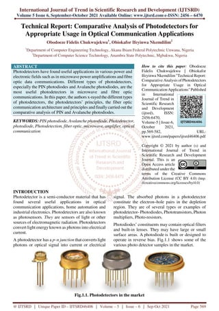
  • 1. International Journal of Trend in Scientific Research and Development (IJTSRD) Volume 5 Issue 6, September-October 2021 Available Online: www.ijtsrd.com e-ISSN: 2456 – 6470 @ IJTSRD | Unique Paper ID – IJTSRD46406 | Volume – 5 | Issue – 6 | Sep-Oct 2021 Page 569 Technical Report: Comparative Analysis of Photodetectors for Appropriate Usage in Optical Communication Applications Obodoeze Fidelis Chukwujekwu1 , Obiokafor Ifeyinwa Nkemdilim2 1 Department of Computer Engineering Technology, Akanu Ibiam Federal Polytechnic Unwana, Nigeria 2 Department of Computer Science Technology, Anambra State Polytechnic, Mgbakwu, Nigeria ABSTRACT Photodetectors have found useful applications in various power and electronic fields such as in microwave power amplifications and fibre optic data communications. Different types of photodetectors, especially the PIN photodiodes and Avalanche photodiodes, are the most useful photodetectors in microwave and fibre optic communications. In this paper, the authors x-rayed the different types of photodetectors, the photodetectors’ principles, the fiber optic communication architecture and principles and finally carried out the comparative analysis of PIN and Avalanche photodiodes. KEYWORDS: PIN photodiode, Avalanche photodiode, Photodetector, photodiode, Photodetection, fiber optic, microwave, amplifier, optical communication How to cite this paper: Obodoeze Fidelis Chukwujekwu | Obiokafor Ifeyinwa Nkemdilim"Technical Report: Comparative Analysis of Photodetectors for Appropriate Usage in Optical Communication Applications"Published in International Journal of Trend in Scientific Research and Development (ijtsrd), ISSN: 2456-6470, Volume-5 | Issue-6, October 2021, pp.569-582, URL: www.ijtsrd.com/papers/ijtsrd46406.pdf Copyright © 2021 by author (s) and International Journal of Trend in Scientific Research and Development Journal. This is an Open Access article distributed under the terms of the Creative Commons Attribution License (CC BY 4.0) (http: //creativecommons.org/licenses/by/4.0) INTRODUCTION Photodetector is a semi-conductor material that has found several useful applications in optical communication applications, home automation and industrial electronics. Photodetectors are also known as photosensors. They are sensors of light or other sources of electromagnetic radiation. Photodetectors convert light energy known as photons into electrical current. A photodetector has a p–n junction that converts light photons or optical signal into current or electrical signal. The absorbed photons in a photodetector constitute the electron–hole pairs in the depletion region. They are of several types or examples of photodetector- Photodiodes, Phototransistors, Photon multipliers, Photo-resistors. Photodiodes’ constituents may contain optical filters and built-in lenses. They may have large or small surface areas. A photodiode is built or designed to operate in reverse bias. Fig.1.1 shows some of the various photo detector samples in the market. Fig.1.1. Photodetectors in the market IJTSRD46406
  • 2. International Journal of Trend in Scientific Research and Development @ www.ijtsrd.com eISSN: 2456-6470 @ IJTSRD | Unique Paper ID – IJTSRD46406 | Volume – 5 | Issue – 6 | Sep-Oct 2021 Page 570 A photodetector is made up of semiconductor materials and absorbs incident photos and convert them into electrons. Fig.1.2 shows the working principle of a photodetector. Fig.1.2. A photodetector working principle A. Principles of Photodetection Photodetection principle is based on two types of photoelectric effects which are as follow:- 1. External photoelectric effect 2. Internal photoelectric effect 1. External photoelectric effect: In external photoelectric effect, electrons become free from the metal surfaces by energy absorption obtained by streams of incident photons. Photomultiplier tube and vacuum photodiode are the implications of external photoelectric effect. 2. Internal photoelectric effect: In internal photoelectric effect, free charge carriers are generated by absorption of incident photons in semi- conductor junction detectors. PIN photodiodes, PN junction photodiodes and Avalanche Photodiodes are typical examples that utilize this effect. A Photodiode works in the following principle- the reverse-biased photodiode is under luminance (incident photons) represents the energy band gap diagram which is absorbed via the window. The absorbed energy raises a bound electron across the band gap from the valance to the conduction band as depicted Fig.1.3. A free hole is left in the valence to the conduction band. Under electric field the generated free charge carriers produce the drift current. Fig.1.3. Photodiode energy band diagram B. Photodiode equivalent circuit The simplified photodiode equivalent model (Fig.1.4) represents the key elements. The irradiance (light intensity) is proportional to current source ID which is in parallel with diode. Performance is dependent upon parasitic components RD and CD can play an imperative role. Fig.1.4. Photodiode Equivalent Circuit
  • 3. International Journal of Trend in Scientific Research and Development @ www.ijtsrd.com eISSN: 2456-6470 @ IJTSRD | Unique Paper ID – IJTSRD46406 | Volume – 5 | Issue – 6 | Sep-Oct 2021 Page 571 C. Modes of Operation of Photodiodes The operating modes of the photodiode include three modes, namely Photovoltaic mode, Photoconductive mode and Avalanche diode mode. Photovoltaic Mode: This mode is also known as zero bias mode, in which a voltage is produced by the lightened photodiode. It gives a very small dynamic range and non-linear necessity of the voltage formed. A photodiode that operates in this mode is usually used as solar or photo-voltaic cell. Photoconductive Mode: The photodiode used in this photoconductive mode is more usually reverse biased. The reverse voltage application will increase the depletion layer’s width, which in turn decreases the response time and the junction capacitance. This mode is too fast and displays electronic noise. Avalanche Diode Mode: Avalanche diodes operate in a high reverse bias condition, which permits multiplication of an avalanche breakdown to each photo produced electron-hole pair. This leads to an internal gain in the photodiode, which slowly increases the device response. D. Basic requirements of a Photodetector for a good performance The basic requirements or properties of a Photodetector to perform well are summarized as follow: 1. Sensitivity at the required wavelength. 2. Efficient conversion of photos to electrons. 3. Responsitivity or fast response to operate at high frequencies. 4. Low noise for reduced errors. 5. Sufficient area for efficient coupling to optical fiber. 6. High reliability. 7. Low cost. 8. Rise time. Other significant photodetecor parameters include the following:- 1. Quantum Efficiency : It is the ratio of primary electron-hole pairs created photon to the photon incident on the diode material. 2. Detector Responsivity: This is the ratio of output current to input optical power. Hence, this is the efficiency of the device. The unit of responsivity is amperes per watt. 3. Spectral Response Range: This is the range of wavelenght over which the device will operate. The spectral response refers to the curve of detector responsivity as a function of wavelenght. 4. Noise Characteristics: This is the level of noise produced in the device. This is critical to the operation of the device at low levels of input light. 5. Response Time: This is a measure of how quickly the detector can respond to variation in the input light intensity. 6. Rise Time : This is the time for the detector output current to change from 10 to 90% of its final value when the optic input power variation is a step. 7. Gain: The Avalanche Photo Device (APD) have more gain than PIN diode due to the effect of impact ionisation as it is operated at high electric field. E. Significance of Photodiodes Photodiodes are unique among light photodetectors in that when illuminated, they generate an output which is proportional to light level. Their characteristics and featurs can be summarised as follows:- 1. Low cost visible and near-IR photo detector 2. Excellent linearity in output photocurrent according to light intensity 3. Fast response times 4. Available in a wide range of packages 5. Low noise 6. Mechanically rugged yet compact and light weight. 7. Available as duals, quads or as linear arrays. 8. Usbale with almost any visible or near infrared light source such as LEDs, neon, fluorescent, incandescent bulbs, lasers, flame sources, sunlight, etc. F. Applications of PIN Photodiodes and Avalanche Photodiodes PIN Photodiode, an example of photodiode, is the most widely used in the following domain or applications: Audio CD players
  • 4. International Journal of Trend in Scientific Research and Development @ www.ijtsrd.com eISSN: 2456-6470 @ IJTSRD | Unique Paper ID – IJTSRD46406 | Volume – 5 | Issue – 6 | Sep-Oct 2021 Page 572 DVD Players Computer CD drives Optical Communication Systems Nuclear radiation detectors Avalanche Photodiode (APD): Avalanche Photodiode (APD) level of gain is of importance for high voltage requirements. They are used in the following domains:- Laser range finders Fast receiver modules for optical data communications High speed Laser scanner ( 2D bar code reader) PET scanner Speed gun Microscopy and particle detection Photodetector is the fundamental element of optical receiver, followed by amplifiers and signal conditioning circuitry. Some other photodiodes are utilised in some applications as follow:- Optical position sensors Beam alignment Laser range finders Photography Analytical Instrumentation Spectroscopy Medical Imaging Instruments Surface characterisation G. Classification or types of Photo detectors There are basically two types of Photodetectors as used in optical communication applications. They types are as follow: 1. Photoconductive detector 2. Junction photodetector 1. Photoconductive detector Photoconductive photodetector is widely known as LDR (Light Dependent Resistor) or photoresistors. It detects the presence of light and its intensity. On light incidence, the electrical conductivity and hence resistance of this device changes from several mega ohms (in dark condition) to few kilo ohms in light condition and thereby detects the presence of light and its intensity. Light dependent resistors, LDRs or photoresistors are often used in circuits where it is necessary to detect the presence or the level of light. They can be described by a variety of names from light dependent resistor, LDR, photoresistor, or even photo cell, photocell or photoconductor. Although other devices such as photodiodes or photo-transistor can also be used, LDRs or photoresistors are particularly convenient electronic components to use. They provide large change in resistance for changes in light level. In view of their low cost, ease of manufacture, and ease of use LDRs have been used in a variety of different applications. At one time LDRs were used in photographic light meters, and even now they are still used in a variety of applications where it is necessary to detect light levels. It is relatively easy to understand the basics of how an LDR works without delving into complicated explanations. It is first necessary to understand that an electrical current consists of the movement of electrons within a material. Good conductors have a large number of free electrons that can drift in a given direction under the action of a potential difference. Insulators with a high resistance have very few free electrons, and therefore it is hard to make them move and hence a current to flow.
  • 5. International Journal of Trend in Scientific Research and Development @ www.ijtsrd.com eISSN: 2456-6470 @ IJTSRD | Unique Paper ID – IJTSRD46406 | Volume – 5 | Issue – 6 | Sep-Oct 2021 Page 573 An LDR or photoresistor is made any semiconductor material with a high resistance. It has a high resistance because there are very few electrons that are free and able to move - the vast majority of the electrons are locked into the crystal lattice and unable to move. Therefore in this state there is a high LDR resistance. As light falls on the semiconductor, the light photons are absorbed by the semiconductor lattice and some of their energy is transferred to the electrons. This gives some of them sufficient energy to break free from the crystal lattice so that they can then conduct electricity; this results in a lowering of the resistance of the semiconductor and hence the overall LDR resistance. Fig.1.5 depict a typical leaded light dependent resistor, its basic structure and symbol while Fig.1.6 shows a typical leaded light dependent resistor. Fig.1.7 depicts the circuit symbols of light dependent resistor, LDR. The process is progressive, and as more light shines on the LDR semiconductor, so more electrons are released to conduct electricity and the resistance falls further. Fig.1.5: Typical leaded light dependent resistor, basic structure and symbol Fig.1.6: Typical leaded light dependent resistor The LDR symbol used in circuits is based around the resistor circuit symbol, but shows the light, in the form of arrows shining on shown in Fig.1.7. By this, it follows the same convention used for photodiode and phototransistor circuit symbols where arrows are used to show the light falling on these components. The light dependent resistor or photo resistor circuit symbols are shown for both the newer style resistor symbol, i.e. a rectangular box and the older zig-zag line resistor circuit symbols. The working principle of LDR is shown in Fig.1.8. Fig.1.7: light dependent resistor symbol Fig.1.8. Light Dependent Resistor (LDR) working principle
  • 6. International Journal of Trend in Scientific Research and Development @ www.ijtsrd.com eISSN: 2456-6470 @ IJTSRD | Unique Paper ID – IJTSRD46406 | Volume – 5 | Issue – 6 | Sep-Oct 2021 Page 574 2. Junction Photodetector There are several types of Junction Photodetectors. They include the following:- P-n junction photodiode PIN photodiode Avalanche photodiode Schottky photodiode Phototransistor P-n Junction Photodiode: In general, p-n junction, as depicted in Fig.1.9, like current rectification, can also be used for light detection purpose. Fig.1.9. P-n junction photodiode The PIN Photodiode: The Pn junction photodiode has two drawbacks: 1. Depletion layer capacitance is not sufficiently small to allow Photodetection at high modulation frequencies (RC time constant limitation). 2. Narrow SCL (at most a few microns). Long wavelengths incidence photons are absorbed outside SCL, low QE. The PIN photodiode can reduce these two problems. The PIN diode derived its name from the fact that it has three main layers. Rather than just having a P-type and an N-type layer, it has three layers such as: P-type layer Intrinsic layer N-type layer The working principle of the PIN diode exactly same as a normal diode. The main difference is that the depletion region, because that normally exists between both the P and N regions in a reverse biased or unbiased diode is larger. In any PN junction diode, the P region contains holes as it has been doped to make sure that it has a majority of holes. Likewise the N-region has been doped to hold excess electrons. The layer between the P and N regions includes no charge carriers as any electrons or holes merge. As the depletion region of the diode has no charge carriers it works as an insulator. The depletion region exists within a PIN diode, but if the PIN diode is forward biased, then the carriers come into the depletion region and as the two carrier types get together, the flow of current will starts. Figs.1.10, 1.11 and 1.12 show the structure of PIN photodiode, Reverse-biased PIN Photodiode and PIN photodiode circuit respectively. Fig.1.13. represents the energy band diagram of PIN photodiode. Applications of PIN Diodes: The main applications of PIN mainly include the following areas:- The PIN diode is used as a high voltage rectifier. The intrinsic layer in the diode offers a partition between the both the layers, permitting higher reverse voltages to be tolerated The PIN diode is used as an ideal radio frequency switch. The intrinsic layer among the P and N layers increases the space between them. This also reduces the capacitance between both the regions, thus raising the level of isolation when the PIN diode is reverse biased. The PIN diode is used as a photodetector to convert the light into the current which takes place in the depletion layer of a photo diode, rising the depletion layer by inserting the intrinsic layer progresses the performance by increasing the volume in where light change occurs.
  • 7. International Journal of Trend in Scientific Research and Development @ www.ijtsrd.com eISSN: 2456-6470 @ IJTSRD | Unique Paper ID – IJTSRD46406 | Volume – 5 | Issue – 6 | Sep-Oct 2021 Page 575 This diode is an ideal element to give electronics switching in applications of electronics. It is mainly useful for RF design applications and also for providing the switching, or an attenuating element in RF attenuators and RF switches. The PIN diode is capable to give much higher levels of consistency than RF relays that are frequently the only other alternative. Fig.1.10. Structure of PIN Diode Fig.1.11. Reverse-biased PIN Photodiode Fig.1.12. PIN photodiode circuit Fig.1.13. Energy Band diagram of PIN photodiode
  • 8. International Journal of Trend in Scientific Research and Development @ www.ijtsrd.com eISSN: 2456-6470 @ IJTSRD | Unique Paper ID – IJTSRD46406 | Volume – 5 | Issue – 6 | Sep-Oct 2021 Page 576 Avalanche Photodiode (APD): The Avalanche Photodiode (APD) is another n+1-I-p+ which provides very high gain 200 and can detect even very low-level of light due to several reasons. This detector is widely used in dedicated optical communication. The thickness of I-region is very large compared with the other region of the device, so incoming light quickly passes through n+ and p layers and spend major time in this region creating large electron and hole pairs. This is known as absorption region of the device. See Fig.1.14. Fig.1.14. Working principle of Avalanche Photodiode Schottky photodiode: Schottky photodiode is one of the simple metal semiconductor junctions. The advantage of this type of photodiode is its high speed which arises from the fact that it is a majority carrier device. And its depletion layer is one sided only (n side). The Schottky photodiode is shown in Fig.1.15. Fig.1.15. Schottky Photodiode Phototransistor: This is a special class of photodetector like the Avalanche Photodiode. Phototransistor, as shown in Fig.1.16, provides high gain; the device on receiving a weak signal amplifies it internally and then passes on its output terminal. Fig.1.16.Phototransistor photodiode working principle
  • 9. International Journal of Trend in Scientific Research and Development @ www.ijtsrd.com eISSN: 2456-6470 @ IJTSRD | Unique Paper ID – IJTSRD46406 | Volume – 5 | Issue – 6 | Sep-Oct 2021 Page 577 2.1. FIBER OPTIC COMMUNICATION SYSTEM A. Fiber Optic Communication System The fiber optic communication is the ideal choice for gigabits and beyond gigabits transmission of data. This type of communication is used to transmit voice, video, telemetry and data over long distances and local area networks (LAN) or computer networks at very fast speed. A fiber optic communication system uses light wave technology to transmit the data over a fiber by changing electronic signals into light. Some exceptional characteristic features of this type of communication system like large bandwidth, smaller diameter, light weight, long distance signal transmission, low attenuation, transmission security, and so on make this communication a major building block in any telecommunication infrastructure. The subsequent information on fiber optic communication system highlights its characteristic features, basic elements and other details. Fig.2.1 depicts the basic fiber optic communication system [1]. Fig.2.1. The basic fiber optic communication system[1] Three Basic Elements of a Fiber Optic Communication System: There are three main basic elements of fiber optic communication system. They are:- Compact Light Source Low loss Optical Fiber Photo Detector Accessories like connectors, switches, couplers, multiplexing devices, amplifiers and splices are also essential elements in this communication system. 1. Compact Light Source The light emitting diodes are used for short distances and low data rate applications due to their low bandwidth and power capabilities. The Laser diode structure is of two types the Can and Frame types as shown in Fig.2.2. Two such LEDs structures include Surface and Edge Emitting Systems. The surface emitting diodes are simple in design and are reliable, but due to its broader line width and modulation frequency limitation edge emitting diode are mostly used. Edge emitting diodes have high power and narrower line width capabilities. Fig.2.2. the Laser Diode Structure For longer distances and high data rate transmission, Laser Diodes are preferred over LED due to its high power, high speed and narrower spectral line width characteristics. But these are inherently non-linear and more
  • 10. International Journal of Trend in Scientific Research and Development @ www.ijtsrd.com eISSN: 2456-6470 @ IJTSRD | Unique Paper ID – IJTSRD46406 | Volume – 5 | Issue – 6 | Sep-Oct 2021 Page 578 sensitive to temperature variations. Nowadays many improvements and advancements have made these sources more reliable. Table 2.1 depicts the comparison/differences between the Laser Diodes and LED according to the variation in the properties. Both these sources are modulated using either direct or external modulation techniques. Table 2.1. The LED versus Laser Diodes 2. Low Loss Optical Fiber Optical fiber is a cable, as shown in Fig.2.3, which is also known as cylindrical dielectric waveguide made of low loss material. An optical fiber also considers the parameters like the environment in which it is operating, the tensile strength, durability and rigidity. The Fiber optic cable is made of high quality extruded glass (si) or plastic, and it is flexible. The diameter of the fiber optic cable is in between 0.25 to 0.5mm (slightly thicker than a human hair). Fig.2.3. Fiber Optic Cable A Fiber Optic Cable consists of four parts. Core Cladding Buffer Jacket Core: The core of a fiber cable is a cylinder of plastic that runs all along the fiber cable’s length, and offers protection by cladding. The diameter of the core depends on the application used. Due to internal reflection, the light travelling within the core reflects from the core, the cladding boundary. The core cross section needs to be a circular one for most of the applications. Cladding: Cladding is an outer optical material that protects the core. The main function of the cladding is that it reflects the light back into the core. When light enters through the core (dense material) into the cladding(less dense material), it changes its angle, and then reflects back to the core. Buffer: The main function of the buffer is to protect the fiber from damage and thousands of optical fibers arranged in hundreds of optical cables. These bundles are protected by the cable’s outer covering that is called jacket. Jacket: Fiber optic cables jackets are available in different colors that can easilymake us recognize the exact color of the cable we are dealing with. The color yellow clearly signifies a single mode cable, and orange color indicates multimode. Types of Optical Fibers: Single-Mode Fibers: Single mode fibers are used to transmit one signal per fiber; these fibers are used in telephone and television sets. Single mode fibers have small cores.
  • 11. International Journal of Trend in Scientific Research and Development @ www.ijtsrd.com eISSN: 2456-6470 @ IJTSRD | Unique Paper ID – IJTSRD46406 | Volume – 5 | Issue – 6 | Sep-Oct 2021 Page 579 Multi-Mode Fibers: Multimode fibers are used to transmit many signals per fiber; these signals are used in computer and local area networks that have larger cores. 3. Photo Detectors The purpose of photo detectors is to convert the light signal back to an electrical signal. Two types of photo detectors are mainly used for optical receiver in optical communication system: PIN photo diode and avalanche photo diode. Depending on the application’s wavelengths, the material composition of these devices vary. These materials include silicon, germanium, InGaAs, etc. B. Photodetectors in Optical Communication According to [2], the fiber optics transmission involves transmission of signals in the form of light from one point to the other. Furthermore, a fiber optic communication network consists of transmitting and receiving circuitry, a light source and detector devices. An optical detector is a device that converts light signals into electrical signals, which can then be amplified and processed. Photodetectors can dictate or determine the performance of a fiber optic communication link. A photodetector acts as an optical receiver in fiber optic communication system. Two purposes of a photodetector in a fiber optic communication system include the following:- 1. For terminal reception of the communication link at the transmitter end, 2. For photoelectric conversion of the relay system. Out of the different types of Photodetectors, the two most commonlyused suitable for fiber optic communication system are:- PIN Photodiode and Avalanche Photodiode (APD). C. Photoelectric detection and optical receiver According to authors in [2], at the transmitting end of the optical fiber communication system, the light source is modulated with a low-frequency baseband electrical signal, and then the modulated light signal is transmitted via the optical fiber. Due to factors such as attenuation and dispersion of optical fibers, when a dimmed signal is transmitted to the receiving end, it becomes weak and has waveform distortion. The role of the optical receiver is to detect the weak light signal first, then convert it into an electrical signal, and then restore to the original baseband signal through amplification, shaping, regeneration, and decoding. Therefore, the core component of the optical receiver is a photodetector. In the entire optical fiber communication system, the photoelectric detection device mainly has two purposes: one is for terminal reception of the communication system, and the upper part of the Fig.2.4 is the schematic diagram of terminal receiving of the digital optical fiber communication system; the second is photoelectric conversion for the relay station. After the signal processing continues to transmit, the lower part (see Fig.2.4) depicts the relay station’s photoelectric conversion process. Fig.2.4. Working Process Diagram of Optical Communication System [2] D. Photoelectric detection principle The photodetector is an optoelectronic device made by utilizing the photoelectric effect of a semiconductor. It converts the change of the optical signal into the change of the photocurrent, and reflects the change rule of the information. According to different conversion parameters, the semiconductor photodetector has two basic
  • 12. International Journal of Trend in Scientific Research and Development @ www.ijtsrd.com eISSN: 2456-6470 @ IJTSRD | Unique Paper ID – IJTSRD46406 | Volume – 5 | Issue – 6 | Sep-Oct 2021 Page 580 types: photoconductive type and photodiode type. The conductance of the photoconductive type detector changes with the change of luminous flux. The photodiode is always operated in the reverse bias state. It belongs to the inner photoelectric effect device, and the incident photon does not directly bombard photoelectrons, but merely raises the internal electrons from the lower energy level to the higher energy level. The differential resistance of the photodetector does not change with the luminous flux, and the generated photocurrent is proportional to the luminous flux. Both types of semiconductor photodetection devices have very fast response speeds, but have their own characteristics and different uses. In optical fiber communication systems, the most widely used photodetector is a photodiode because of the small size and long life of such detectors. 3.1. COMPARATIVE ANALYSIS BETWEEN PIN PHOTODIODE AND AVALANCHE PHOTODIODE PHOTODETECTORS A. Comparison between PIN photodiode and Avalanche Photodiode (APD) as used in Fiber Optic Communication According to the [3], PIN photodiodes and Avalanche Photodiodes (APD) are used as receivers to facilitate fiber optic networks. Often, they provide extremely high-speed internet access or receive telephone and digital television signals. The chief overall advantage of optical technology is its high data transfer rate; PIN and APD receivers are both designed for such applications. However, there have different or distinct technologies. Avalanche photodiodes (APDs) are widely used in laser-based fiber optic systems to convert optical data into electrical form. They are high-sensitivity, high-speed semiconductor light sensors. The main advantage of the APD is that it has a greater level of sensitivity compared to PIN photodiode. The avalanche action increases the gain of the diode many times, providing much higher sensitivity. However, an APD requires a higher operating voltage. In addition, the term avalanche refers to the output being non linear; as a result, APDs also produce a higher level of noise than a PIN diode. Also APDs, unlike PIN devices, need a high reverse bias condition to work. That permits avalanche multiplication of the holes and electrons created by the initial electron-hole pairs. APDs have an internal region where electron multiplication occurs by application of an external reverse voltage. The resultant gain in the output signal means that low light levels can be measured at high speed. For silicon, an APD diode will typically require between 100-200 V, and with that voltage they will provide a current gain effect of roughly 100 V, resulting from the avalanche effect. Some diodes that use specialized manufacturing processes enable much higher bias voltages of up to 1,500 V to be applied. The gain levels increase when higher voltages are applied, therefore the gain of these avalanche diodes can rise to the order of 1,000. That provides an advantage in solutions where sensitivity is important. Typical applications for APDs are laser rangefinders and long-range fiber optic telecommunication, as well as positron emission tomography and particle physics. APD arrays are increasingly commercially available. The avalanche photodiodes are not as widely used as their PIN counterparts. They are generally used where the level of gain is important and because of the high voltages required and lower reliability, they are often less convenient to use than PIN. A PIN diode is a type of diode that has a wide, undoped intrinsic semiconductor region between a p-type semiconductor and an n-type semiconductor region. There is where it derived its name PIN. Because of their applications for ohmic contacts, the p-type and n-type regions are typically heavily doped. The main difference between a PIN diode and an ordinary p-n diode is the wide intrinsic region in the PIN diode p-n junction. Because of this, PIN diode is inferior to the normal p-n diode as a rectifier. PIN diode is very suitable for attenuators and RF switches because of its wide intrinsic region. It is equally very suitable as photodetectors and applied very much in high-voltage power electronics applications, such as a high-voltage rectifier. Higher reverse voltages are tolerated in PIN diode because its intrinsic region provides a greater separation between the p and n regions. PIN diodes are applied in RF scenarios where the capacitance levels are low. The switching and variable resistance properties of PIN diodes make them well adapted in switching and variable attenuator applications. The comparative differences between Avalanche Photodiode and PIN photodiode are summarized in Table 3.1.
  • 13. International Journal of Trend in Scientific Research and Development @ www.ijtsrd.com eISSN: 2456-6470 @ IJTSRD | Unique Paper ID – IJTSRD46406 | Volume – 5 | Issue – 6 | Sep-Oct 2021 Page 581 TABLE 3.1. Comparative differences between Avalanche Photodiode and PIN photodiode S/N PIN photodiodes Avalanche Photodiodes 1. It uses a lower reverse biased voltage. It uses a higher reverse biased voltage. 2. It produces a lower level of noise It produces a higher level of noise 3. It requires a lower operating voltage It requires a higher operating voltage 4. It is a passive microwave diode (not used in power generation or amplification) It is an active microwave diode. 5. It operates at a maximum frequency of 100MHz as a rectifier and up to 150 GHz maximum as a microwave diode. It operates at a frequency in excess of 200 GHz as a microwave diode. 6. It does not exhibit negative resistance characteristics unlike the Avalanche Photodiode, Tunnel diode, IMPATT and TRAPATT diodes. It exhibits negative resistance characteristics like the Tunnel diode, IMPATT and TRAPATT diodes. 7. It is not used in power generation or amplification. It is used on power generation or amplification. 8. It provides a lower sensitivity in fiber optic communication systems. It produces a much higher sensitivity because of avalanche action (about 10-150 times higher than PIN photodiode) in fiber optic communication systems 9. It has a slower response time (5 ns). It has a much faster response time (2 ns). 10. It cannot be used as for higher pulse modulation rates in fiber optic communication systems than the APD. It can be used for higher pulse modulation rates for reception in fiber optic communication systems than the PIN photodiodes. 11. It has a better linear output. It has a non-linear output. 12. It has a wider usage and applications. It a narrower usage and applications and are used only where level of gain is important. 13. It is easier and more convenient to use. It is less convenient to us because of higher voltage requirement and less reliability. 14. It is used as weaker rectifier, attenuator, RF switches, photodetectors and high- voltage power electronics applications, such as a high-voltage rectifier. It is used in laser rangefinders and long-range fiber optic telecommunication, as well as positron emission tomography and particle physics Similarities between PIN photodiode and Avalanche Photodiode: The similarities between the two photodiodes are as follow:- 1. They are both used in microwave power switching, limiting and modulation. 2. They are made from the same semi-conductor materials. 3. They both operate in reverse-biased mode. 4. They are both used in fiber optic communication in optical receiver as photodetector. SUMMARY AND CONCLUSION Photodetectors such as Avalanche Photodiodes (AVDs) and PIN photodiodes are very important Photodetectors in fiber optic communication systems as well as other wide range applications. Both of them operate at different working principles and can be used or applied in fiber optic communication system as optical receivers and relay processing elements. They have different differences in operation and applications. PIN photodiode operates at a lower reverse biased voltage compared to APD which operates at a higher reverse biased voltage. PIN photodiode/photodetector is easier and more convenient to use compared to APD but APD has a much higher sensitivity because of avalanche action. PIN photodiode is much reliable and does not require a very high operating voltage like the APD. APD is always applied where higher gain is desirable. References [1] Elprocus. com. “What are the Basic Elements of a Fiber Optic Communication System?” . Accessed online at https://www.elprocus. com/basic-elements-of-fiber-optic- communication-system-and-its-working [2] FOT Blog, June 29, 2018. “Two major uses of photodetectors in optical communication systems”. Accessed online at https://www.fiberoptictel.com/two-major-uses-
  • 14. International Journal of Trend in Scientific Research and Development @ www.ijtsrd.com eISSN: 2456-6470 @ IJTSRD | Unique Paper ID – IJTSRD46406 | Volume – 5 | Issue – 6 | Sep-Oct 2021 Page 582 of-photodetectors-in-optical-communication- systems/ on August 16th 2019. [3] Electronics360globalspec.com, “Industrial Electronics: PIN vs. APD: Different Sensitivity, Different Applications”, 21st November 2017. Accessed online at https://electronics360.globalspec.com/article/10 397/pin-vs-apd-different-sensitivity-different- applications on August 5, 2019.