SlideShare ist ein Scribd-Unternehmen logo
1 von 21
PRESENTATION SUMMARY FOR TECHNICAL RECRUITMENT STAFFINGSHAWN E. JACKSON, CHEMICAL ENGINEER 1/17/2011 1
CAREER SUMMARY A recognized successful mid-level engineering and clinical professional with professional background and education across several industries including petroleum, high technology integrated electronics, biotechnology, clinical healthcare, and nanotechnology.  Career experiences in Process Engineering and Development, Process Improvement, Process Optimization and Control, Process Safety, Project Engineering, and Project Leadership and Supervision.  Proven ability to bridge technology and business goals to provide productive solutions on time or prior to a business deadline.  Demonstrated ability to implement technological solutions that harness applied scientific theory to solve a given problem.  Experienced Team Builder with expertise in building Customer Relations across multi-disciplinary and cross functional teams, including multi-cultural Team Environments in international business organizations at the global level.  Excellent communicator with proven technical writing and presentation skills.  Quick learner that rapidly adapts to emerging technologies with the ability to change dynamically with business goals and objectives. 1/17/2011 2
EDUCATION AND HONORS - ENGINEERING University of Arizona  Bachelor of Science Degree in Chemical Engineering, Chemical Engineering  1994 – 1998  ● Baird and Honors Scholarship Recipient 	● Proficient with Chemical Engineering Process Simulation Software 	● Chemical Engineering Software Problem Solving Applications for Unit Operations 	● Chemical Engineering Unit Operations and Science 	● Hazardous Waste Treatment Unit Operations 	● Chemical and Analytical Laboratory Methods 	● FORTRAN Programming, Visual Basic, BASIC 	● Operating Systems, Software Applications  Arizona State University N/A, Electrical Engineering  1997 – 1999  ● Started Program Requirements for a Master of Science Degree In Electrical Engineering with an Emphasis In Solid State Electronics 	● Completed courses in Semiconductor Processing and Device Theory  Motorola University - Corporate Training Institute N/A, Corporate Manufacturing and Leadership Training  1997 – 1999  Corporate Training Courses:● Manufacturing Excellence and (Quality) Improvement● Six Sigma Quality Training● JMP Statistical Analysis Software for DOE, Data Analysis and Six Sigma Applications● Design of Experiments (DOE)● Process Capability● Measurement Capability, Gage R&R Studies● Leadership Training – Steven Covey: 7 Habits of Highly Effective People; Dale Carnegie; Dennis Deaton  1/17/2011 3
CAREER CONTRIBUTIONS AND ACHIEVEMENTS ● Manufacturing Excellence Awards ● Engineering Project Management  ● Engineering Project Supervision ● Process Developments ● Process Implementations ● Process Improvements ● Applied Engineering Methods ● Process Characterization ● Quality Initiatives and Implementation ● Continuous Improvement Initiatives ● Quality Standards Compliance ● Direct Contributions in IC Manufacturing Success ● Reliability of Scientific and Clinical Results ● Proven Leadership Success ● Team Building for Success ● Engineering Technical Publication ● Technical Process Change Approvals ● Technical Writing and Presentations ● Communication Skills ● Continuous Education and Excellence ● Exceptional Performance Reviews ● Exceptional Salary History Record ● Cost Savings ● Philanthropic Activities 1/17/2011 4
PROFESSIONAL DEVELOPMENT AND LEADERSHIP TRAINING International Leadership Role in a High Technology Company for Next Generation IC Technologies  Leadership Training – Steven Covey: 7 Habits of Highly Effective People; Dale Carnegie; Dennis Deaton Manufacturing Excellence and Statistical Process Control Methods Management Quality Standards for Continuous Improvement: Six Sigma, ISO9000, ISO9001 American Institute of Chemical Engineers 1/17/2011 5
ADDITIONAL COMPETENCIES ● Manufacturing Process Monitoring and Control Software  ● JMP Statistical Analysis Software Applications ● FORTRAN Programming, Visual Basic, BASIC ● Computer Literacy in All Respects ● Operating System and Database Management Experience ● Specialized Experience in Semiconductor Process Equipment and External Interface Systems for complete designed and built Integrated Circuits	 ● Specialized Experience in Semiconductor Analytical Methods and Metrology Process and External Interface Systems for Process Characterization ● Proficient with Chemical Engineering Process Simulation Software ● Chemical Engineering Software Problem Solving Applications for Unit Operations ● Semiconductor Process Modeling Software ● Electrocardiography Monitoring and Interpretation ● Medical Laboratory and Patient Care Experience ● Chemical Engineering Unit Operations and Science ● Hazardous Waste Treatment Unit Operations ● Chemical, Analytical and Medical Laboratory 	Methods	 ●Material and Spectroscopy Analysis Techniques ● Conversational Japanese, French and Spanish 1/17/2011 6
DIRECT EXPERIENCE IN CHEMICAL ENGINEERING & PROFESSSIONAL WORKS DIRECT EXPERIENCE IN CHEMICAL ENGINEERING & PROFESSSIONAL WORKS ● Bachelor of Science Degree in Chemical Engineering with 8 years of Applied Chemical Engineering Experience.  12 years of experience and education with emphasis in chemical engineering applications. ● Industry experience: Semiconductor Manufacturing Process and Development; Nanotechnology Research and Development; Industrial Waste Treatment and Municipal Waste Treatment; Regulatory Standards: OSHA, EPA, ADEQ and Phoenix City Code for Safety Standards, Semiconductor Equipment and Materials International Standards, and ASTM Standards for Government Space and Military Testing Requirements. ● 6 years of Solid State Microelectronics Manufacturing and Process Development Experience. ● Specific and direct experiences in engineering problem solving and problem resolutions in process technologies and modules of integrated circuit manufacture with most notable experiences CVD processes; CVD, Diffusion, Implantation and Photolithography Metrology; Defectivity, Yield Enhancement, and Inspection Technologies; Diffusion Process; Implantation Process and Electrical Device Parametrics; Rapid Thermal Processing; Photolithography Process; Wet Process Engineering; Wafer Surface Cleaning and Chemical Mechanical Polish Process Technologies; and Single Crystal Growth Czochralski (CZ) Processes.  GaAs and Si device process, manufacturing and process development experiences. ● Medical Laboratory experience in Microbiology, Chemistry, Hematology, Urinalysis, Coagulation, and Blood Bank.  5 years experience and education with Clinical Solutions, Diagnostic Equipment, Technology and In-Vitro Diagnostics methods and applications. 	 ● 7 years of Project Engineering and Process Engineering responsibilities, with long term success track record in providing deliverables and meeting business goals prior to or on time to a given deadline. ● National and International Travel experience (up to 75%) with global leaders in the microelectronics industry in an Applications Engineering role. ● Professional References and further specific details related to professional experiences available upon request and over http://www.LinkedIn.com/in/shawnejackson. 1/17/2011 7
CAREER HISTORY WITH MAJOR ACCOMPLISHMENTS - Nanotechnology 2008 – 2009; Materials and Electrochemical Research (MER) Corporation; Tucson, AZResearch Engineer with the Nanotechnology / Advanced Composite Materials Group ● Maintained the continuous chemical vapor deposition reactors for nanotube production processing and  films deposition for advanced composites research and development applications; including process characterization, improvement and optimization, safety, process monitoring and control via Labview Software Process Control applications, process analysis and sample preparation for material, optical and electrical spectroscopy research methods, and input for design improvements.  Improved chemical delivery of precursors to process reactors and reaction kinetics via process and reactor upgrades to include modifications to automated process control of syringe pumps, upgrades to HPLC pumps; design improvements to liquid reactant input piping and thermal control process; and liquid and vapor phase catalysis control with reactor column input design improvements. ● Acquired experience in research and production Chemical Vapor Deposition (CVD) thin film processes for double wall (DWNTs), single wall (SWNTs), multi-wall carbon nanotubes (MWCNTs) and SiC-CVD deposited films for advanced composite material applications and development projects for the United States Department of Defense and NASA Space System Projects.  Strengthened experience in materials, optical and electrical spectroscopy analysis methods via Thermogravimetric Analysis (TGA), Scanning Electron Microscopy (SEM), Energy Dispersive X-Ray Spectroscopy (EDS), Near-IR Spectroscopy (N-IR) and research methods for material characterization with Raman Spectroscopy (Raman) and Tunneling Electron Microscopy (TEM). ● Achieved a process improvement of 425% with respect to continuous process reactor up-time.  Determined root causes of defective chemical vapor deposited nanotube films and optimum thin film growth rates per time and reactant input concentration.  Engineered corrective actions to prevent reoccurrence of defective thin film properties and to ensure constancy in film electrical and material characteristics for advanced development applications and to deliver thin film material orders to United States Department of Defense customers on schedule.    ● Generated a process mass balance coincident with the process monitoring database to quantify and track efficiency of the reaction kinetics and thermodynamic conversion of reactants input to system to achieve desired products.  Analyzed gas phase products via Mass Spectroscopy in-situ methods, and solid phase products via TGA and SEM methods.   ● Enhanced Composite and Mechanical Strength Properties of Advanced C-Fiber Composites by over 40% via experimentation and generation of process development methods for production of Nanotube Reinforced Resins, integrating and improving process steps for building Nanotube Reinforced Advanced Composites, and adhering to ASTM Standards for high technology United States Space and Military applications.  ● Responsible for vendor relations and suppliers of reactor chemicals, reactor consumables, reactor parts, cost controls, process upgrade part specifications and design criteria, material specifications, research into design improvements to existing configurations while developing industry supplier relationships, while maintaining continuous reactor production requirements to filling customer orders and internal research requirements. 1/17/2011 8
CAREER HISTORY WITH MAJOR ACCOMPLISHMENTS – Semiconductor Processing2000 – 2001; Accretech USA, Inc. or TSK America, Inc. – U.S. Division of Accretech or Tokyo Seimitsu Co. (TSK), LTD.; San Jose and Milpitas, CAApplications Engineer with Semiconductor Equipment Division, Applications Engineering Group ● Managed next generation Brightfield Patterned and Unpatterned Wafer Inspection Systems Yield Enhancement Applications, Equipment and Software System process integration, facilities installation, system calibration, and capability projects for high volume, high technology integrated circuit manufacturers throughout the United States and Worldwide locations (Micron Technology, Infineon Technologies, Texas Instruments, Intel corporation, Advanced Micro Devices – GlobalFoundries Inc., IBM, NEC, Toshiba, and others).  Bridged technology and business goals to provide productive manufacturing engineered yield improvements and cost savings with reduction in defect density across manufactured device technologies.  Applied engineering applications approaches to detect defect densities on the order of greater than 100% of previous detection methods at critical process steps with the potential net effect of reducing cost for yield loss of next generation electrical device circuits with stricter tolerances and critical dimensions on the same order of magnitude. ● Performed Customer Demonstrations of Brightfield Inspection capabilities.  Provided feedback and engineering evaluations related to overall process integration and system performance, theoretical and practical design strengths and limitations, and customer satisfaction to Worldwide Divisions of our parent company and the Customer including reports and presentations to Worldwide Semiconductor Industry Association (SIA) Manufacturers and Process Development Groups, our Equipment System Development Division, our Application Engineering Groups and Corporate Managers. ● Responsible for all competing wafer inspection technologies, industry developments, and application alternatives at current and next generation design rules and semiconductor process roadmap for technology innovation and integration of our equipment to device and yield engineering approaches to solving process development and manufacturing challenges.  Acquired a strong background in KLA-Tencor and industry competing inspection and yield management systems and the worldwide manufacturing defect challenges. 1/17/2011 9
CAREER HISTORY WITH MAJOR ACCOMPLISHMENTS – Semiconductor Processing2000 – 2001; Accretech USA, Inc. or TSK America, Inc. – U.S. Division of Accretech or Tokyo Seimitsu Co. (TSK), LTD.; San Jose and Milpitas, CAApplications Engineer with Semiconductor Equipment Division, Applications Engineering Group ● Applications experience with the following defectivity-inspection equipment and yield management systems: -Win-Win50 Confocal Brightfield Patterned and Unpatterned Wafer Inspection Systems (footprints for 150-200mm and 200-300mm platforms).-Win-Win50 on/off-line Auto Defect Classification (ADC).-JVC Scanning Electron Microscope (SEM) Review tools and Auto Defect Classification (SEM-ADC) System (200mm and 300mm platforms). -Wafer Inspection Systems: KLA-Tencor Surfscan SP and SP2 series. -Yield Management Systems: KLA-Tencor Klarity Bitmap, Klarity Defect, ACE XP, Spatial Signature Analysis (SSA). ● Familiarity and up to working knowledge (experience) of application and use of these competing technologies for direct defect inspection capability evaluations and process specific applications for defect reduction in manufactured integrated circuits: -Brightfield Patterned Wafer Inspection Systems: KLA-Tencor Stealth (23XX series, 28XX series currently). -Darkfield Patterned Wafer Inspection Systems: KLA-Tencor AIT XP (Puma 91XX and 9500 series currently). ● Characterized complete system capabilities, documented results and wrote technical reports and documentation related to system capability and input into Equipment Manuals for Operation, Calibration, Maintenance and Facilities Integration of our Defect Inspection Technology Equipment for internal and customer training purposes.  Provided technical input and training for Applications Engineering and Technical Staffing.  Interviewed potential candidates for technical staff placement up to the Applications Engineering level and provided input into hiring decisions for our U.S. Division. ● National and International Travel experience (up to 75%) with global leaders in the microelectronics industry in this Applications Engineering role.  Lived abroad in Tokyo, Japan performing work for global Semiconductor Industry Association (SIA) Customers and Tokyo Seimitsu Co. (TSK) Japan, LTD., TSK Micro Technologies Co., LTD. (MTC – a subsidiary of TSK) and in Dresden, Germany for Tokyo Seimitsu Co. (TSK) Europe, GmbH. 1/17/2011 10
CAREER HISTORY WITH MAJOR ACCOMPLISHMENTS – Semiconductor Processing  1996–1999; Process Engineer at Freescale Semiconductor or Motorola, Inc., Semiconductor Products Sector Process Engineer with the Chemical Vapor Deposition Engineering Group ● In the Chemical Vapor Deposition Process Engineering Group, responsible for manufacturing sustaining support and off shift leadership support of technical personal with responsibilities to preventing product losses, deviations from safety standards, keeping equipment and processes running continuously while minimizing down time and maximizing wafer throughput, ensuring staff members understand and follow specifications and standard operating procedures, and discovery of engineering opportunities for process improvements and innovation.  In addition, apply knowledge of engineering principles, theory and applied statistical methods to daily and long term success of product improvement initiatives and sustainment.  Directly responsible for all dielectric, chemical vapor deposited films processes; dielectric, chemical vapor deposition films metrology; and film thickness metrology process requirements for off shift manufacturing, while applying corrective actions to out of control process excursions.  ● Chemical Vapor Deposition Equipment and Process Experience: -Applied Materials Producer PECVD, SACVD; Dielectric Deposition: USG (TEOS) Processes, PSG Process.-Watkins Johnson APCVD; Dielectric Deposition: BPSG Process, TEOS gap fill Process.-Film Thickness Metrology: Prometrix series; Doping Concentration Metrology: Rigaku XRF; Film Stress Metrology. 1/17/2011 11
CAREER HISTORY WITH MAJOR ACCOMPLISHMENTS – Semiconductor Processing  1996–1999; Process Engineer at Freescale Semiconductor or Motorola, Inc., Semiconductor Products SectorProcess Engineer with the Diffusion Process Engineering Group ● In the Diffusion Process Engineering Group, responsible for a process characterization and technology transfer project that included evaluation of optical and electrical properties of gate dielectric properties for non-volatile flash memory (NVM-Flash) process integration.  Characterized the optical and electrical properties of an oxide/nitride/oxide (ONO) film stack for modified, high K dielectric constant process with a Keithley Instruments – Quantox, Non-Contact Gate Oxide Monitoring System, and Rudolph Ellipsometers, including defining diffusion processes for Gate Oxide Diffusion and Low  Pressure Chemical Vapor Deposition (LPCVD) Nitride on Silicon Valley Group (SVG) Furnaces and Reactors.  Further evaluation of the process included film etch rate, analytical methods of Secondary Ion Mass Spectroscopy (SIMs) and Tunneling Electron Microscopy (TEM) to show high K film qualities at oxide/nitride/oxide interfaces and to determine the top oxide diffusion “punch-through” characteristics of the ONO process. ● Diffusion Equipment and Process Experience:-Silicon Valley Group (formerly a subsidiary of ASM Lithography Holding N.V.) Diffusion Furnaces; Gate Oxide Diffusion Processes, LPCVD Process. -Rudolph Technologies, Ellipsometers ; Keithley Instruments, Quantox Non-Contact Gate Oxide Monitoring System. 1/17/2011 12
CAREER HISTORY WITH MAJOR ACCOMPLISHMENTS – Semiconductor Processing  1996–1999; Process Engineer at Freescale Semiconductor or Motorola, Inc., Semiconductor Products SectorProcess Engineer with the Yield Enhancement Engineering Group ● In the Defectivity and Yield Enhancement Process Engineering Group, responsible for root cause analysis and determination of process deviations and process changes for device yield improvement and cost savings.  Recommendations and process change board approvals led to defect reduction of 30% within the double poly capacitor process module and cost savings of over $100K annually.  Received a Manufacturing Excellence Award for project contributions from Motorola Semiconductor Products and Services Group. ● Defectivity and Yield Management Process Equipment Experience: - KLA-Tencor Defectivity and Inspection Systems (3200 series, Brightfield Inspection Technology); KLA-Tencor Defect Review Station (2540 series). - Furthered experience with Photolithography (Cannon i4 and Nikon), Etch (Teagal), Wafer Cleans and Brush Scrub Process Equipment with respect to defectivity excursions at current design rules and equipment configurations specific to process designed criteria. 1/17/2011 13
CAREER HISTORY WITH MAJOR ACCOMPLISHMENTS – Semiconductor Processing  1996–1999; Process Engineer at Freescale Semiconductor or Motorola, Inc., Semiconductor Products SectorProcess Engineer with the Implant Engineering Group ● In the Ion Implantation Process Engineering Group, responsible for and delivered, on time, the installation of two medium current implantation process technologies to increase current manufacturing throughput of compound semiconductor products by 150% for all production implant processes.  Experienced with Ion Implant Equipment installation and safety standards.  Responsible for setup, characterization and optimization of all the new generation ion implant and RTP process recipes; performed device analysis to determine dose and energy sensitivities of the ion implanter systems and temperature sensitivities of the rapid thermal process (RTP) systems for process integration and tool matching to existing ion implantation and RTP tool sets. ● Ion Implantation Equipment and Process Experience: - Eaton Corporation (Axcelis Technologies Inc.) 8250 and 6200 Medium Current Implantation process technologies including residual gas analyzer (RGA) process monitoring system equipment for ion implant species control during Be and H implantation processes. - Rapid Thermal Processing (RTP) equipment and process.  Thermawave Implantation Metrology process. 1/17/2011 14
CAREER HISTORY WITH MAJOR ACCOMPLISHMENTS – Semiconductor Processing 1996–1999; Process Engineer at Freescale Semiconductor or Motorola, Inc., Semiconductor Products Sector Process Engineer with the Photolithography Engineering Group ● In the Photolithography Process Engineering Group, completed manufacturing process development and equipment integration for scaled up manufacturing efforts.  Responsible for measurement and process capability studies, quality improvement, statistical process control (SPC) and process control for several process engineering improvements.  Investigated critical dimension (CD) and Overlay control methods and technology and was responsible for a complete equipment upgrade, transfer and installation of an optical CD and Overlay tool, including complete release of all process recipes at after develop inspect (ADI) and after cleans inspect (ACI, post etch), complete training of all factory staffing and completion of all technical specifications for operation, troubleshooting, and procedures for process control.  Developed  a dual polymer, Bilayer liftoff process at the gate layer with the photolithography and device development groups.  Responsible for all photolithography equipment process developments, including evaluation of films, thickness requirements, exposure relationships, and develop processes.  Co-authored a technical publication in Motorola Proceedings for the latter process and presented findings at the Annual Motorola Technical Enrichment Matrix.    ● Photolithography Equipment and Process Experience: - Vapor Prime Process Equipment, Silicon Valley Group 8600 Coater and 8600 Developer Tracks, Prometrix 7XXX series Film Thickness Metrology tools, BioRad Quaestar 1 and 5 CD and Overlay Metrology tools, Canon i4 and i1 Photolithography Steppers, Phillips Scanning Electron Microscope (SEM) and competing SEM technologies for process alternatives (Hitache and KLA CD-SEM technologies), Defectivity Inspection Microscopes, Analytical Lab Atomic Force  Microscope (AFM) analysis techniques. 1/17/2011 15
CAREER HISTORY WITH MAJOR ACCOMPLISHMENTS – Semiconductor Processing  1996–1999; Process Engineer at Freescale Semiconductor or Motorola, Inc., Semiconductor Products Sector Process Engineer with the Wet Chemical Process / Chemical Mechanical Polish Engineering Group ● In the Wet Chemical Process / Chemical Mechanical Polish Engineering Group, characterized starting Si substrate material (bare wafer) wet chemical cleaning and brush scrub process technologies for metal and particulate contamination levels, post chemical mechanical polish process, prior to shipment to all Motorola SPS factories.  Developed and implemented a statistical process control monitoring system to control Si substrate quality and reliability metrics related to  substrate metal and particulate contamination.  Established SPC control charts, out of control action plans, process specifications and trained all sector staffing on proper control plan and new equipment integration plans for laser scanning inspection technologies.  Established a database management system and programming solution to providing real time or daily process performance with respect to handling and manipulating large data sets for SPC and control applications.  ● Wet Chemical Process / Chemical Mechanical Polish Equipment and Process Experience: - Bold Cleaning Technologies (automated, batch, wet chemical cleans process technologies) and previous generation wet process cleaning technologies, Wafer Brush Scrub Process technologies, KLA-Tencor Surfscan 6XXX series laser scattering inspection technologies, electrical grade resistivity inspection technologies, Analytical Laboratory Techniques and Equipment for Total X-Ray Flouresance (TXRF) analysis techniques. 1/17/2011 16
CAREER HISTORY WITH MAJOR ACCOMPLISHMENTS – Semiconductor Processing1996; Texas Instruments, Inc. (now TriQuint Semiconductor); Dallas, TXProcess Engineer Co-op with the Wet Chemical Process Engineering Group in the Gallium Arsenide (GaAs) Operations Division of the Defense Systems and Electronics Group (DSEG) ● In the Wet Chemical Process Engineering Group, responsible for oversight and deliverables towards four process engineering manufacturing and development project initiatives while taking direction from the process engineering manager and senior process engineer staffing.  Experimented and developed the batch process conditions and wet etch rates for an electrochemical plated metal removal chemistry.  Experimented with environmentally safer wet etch chemicals via the Environmental Protection Agency (EPA) chemical replacement and reduction plan to remove toxic compound chemical solutions from mainstream semiconductor manufacturing methods, thereby reducing potential and real long term human exposure effects and environmental contamination concerns.  Coincident with the former EPA Toxic Chemical Reduction and Replacement Plan for US manufacturers, determined de-ionized (DI) water factory usage related to wet chemical batch process technologies for reduction feasibility analysis.  Finally, converted all process programs on a photoresist stripper to handle two different wafer diameters during standard compound semiconductor manufacturing process operations seamlessly. 1/17/2011 17
CAREER HISTORY WITH MAJOR ACCOMPLISHMENTS – Clinical Medical and Laboratory2006 – 2008; Carondelet Health Network; Tucson, AZLaboratory Technical Assistant with the Clinical Laboratory; Patient Care Technician with the Medical Units at St. Mary’s and St. Joseph’s Hospitals ● Dedicated to the highest standards of quality and excellence in healthcare from a Clinical and Patient perspective.  Conformed, without deviation or error, to clinical lab and patient care training procedures and protocols as outlined through corporate training and government regulatory standards such as the Joint Commission on the Accreditation of Health Care Organizations.  Maximized turn around times of patient clinical test specimens while ensuring the reliability of test results.  Meticulously followed scientific and clinical logic to prioritize objectives and specimen processing in a high volume clinical laboratory environment.   ● Continuously experienced and educated in the clinical laboratory functional disciplines; including in depth experience in Microbiology, Hematology, Urinalysis, Coagulation, Chemistry and Blood Bank.  Maintained these standards through continuous education in relevant degree related coursework, annual review of all specifications and procedures, knowledge based testing in the functional disciplines, continuous education and practice to maintain current with highest quality patient care interventions and procedures and applying problem solving strategies to daily work activities.   ● Specialized in Patient Care Technician competencies in key medical units to be capable of assisting in every major medical unit of the hospital.  Focused on Cardiac Medicine and Nursing science and procedures with additional knowledge based training and experiences primarily in the Medical Surgery, Rehabilitation and Orthopedic Units with assignments delegated from the Central Resource Staffing Team.  Emphasized strong team building and professional relationships with colleagues across the cross functional disciplines within the Hospital Network.  Fully capable of resuscitating victims of respiratory arrest, cardiac arrest, blocked airway and drowning.  Competent in identifying and understanding dysrhythmic heart functions and the associated nursing interventions related to a given deviation from normal heart rhythmic functioning. 1/17/2011 18
CAREER HISTORY WITH MAJOR ACCOMPLISHMENTS – Clinical Medical and Laboratory 2002 – 2006; Tucson Medical Center; Tucson, AZMicrobiology Laboratory Technical Assistant with the Microbiology Clinical Laboratory ● Acquired in depth experience with sample preparation and in-vitro diagnostics methods for Microbiology laboratory test specimens.  Prepared quality control samples for microbiological pathogen growth and water quality standards testing.  Resolved technical issues related to medical lab testing methods with the medical and clinical laboratory staff.  Independently prioritized workflow and test sample preparation in a 700 bed hospital. ● Operation of microbiological equipment and instruments necessary to perform high-volume microbiological tests.  Recognize equipment malfunction and follow corrective actions using established protocols to ensure patient test samples are not compromised.  Monitored Microbiology Lab equipment and environment to ensure highest quality specimen integrity is constantly maintained through the growth and test cycles of the given specimen.  Improved aerobic and anaerobic gas usage for cost savings on an order of 10% overall reduction in losses. 1/17/2011 19
CAREER HISTORY WITH MAJOR ACCOMPLISHMENTS – Industrial and Municipal Hazardous Wastewater Treatment  1990-1991; Tri-Star, Inc.; Phoenix, AZProcess Engineering Intern with the Process Engineering Group ● Responsible for pre-industrial hazardous waste treatment processes in metal finishing and electroplating process operations, including treatment of complex metal salts and cyanide contaminated waste streams prior to safe effluent discharge to the municipal waste treatment plants. ● Maintained continuous and batch treatment chemical processes for cyanide destruction and metal salt reduction while recovering reusable metal wastes from the industrial processes via filter press and chemical flocculation processes. ● Performed batch tank recovery operations of metal finishing and electroplating baths to optimize process quality of finished products and adhere to Aerospace Industry and United States Military design specifications. ● Constant regulatory compliance achieved and improved upon by adhering to strict guidelines from the United States Occupational Safety and Health Administration (OSHA), the Environmental Protection Agency (EPA), Arizona Department of Environmental Quality (ADEQ), and Phoenix City Code for discharge to municipal waste streams. ● Certified by the State of Arizona for Grade One Wastewater Treatment Plant Operation. 1/17/2011 20
PROFESSIONAL EMPLOYMENT HISTORY Relevant Chemical Engineering & Professional Experiences and Corporate Employers: ● 7/2008-Present; Seeking New Opportunities in Professional Endeavors and Employment; Experienced Research, Applications, and Process Engineer & Experienced Clinical Medical Professional. Experienced and/or knowledgeable in some areas of State and Federal Civil Legal Procedures.  Seeking new opportunities in a corporate role with related technical responsibility to my background and experience sets.  Seeking new business ventures or consulting opportunities.  Pursued or pursuing several legal aspects of non-engineering related business matters that I must lead and close.                                                                                         .Industry: Research, Engineering, Technical and Legal Industries. ● 10/2008 – 9/2009; Materials and Electrochemical Research (MER) Corporation; Tucson, AZ; Research Engineer with the Nanotechnology / Advanced Composite Materials Group. Industry: Defense Systems and Aerospace Industry; U.S. Department of Defense, U.S. Space Systems (NASA), and Private Industry Corporations. ● 5/2006 – 7/2008; Carondelet Health Network; Tucson, AZ; Laboratory Technical Assistant with the Clinical Medical Laboratory Units; Patient Care Technician with the Patient Care Units in 2 hospitals. Industry: Clinical Medical, Biological Sciences and Healthcare. ●12/2002 – 8/2006; Tucson Medical Center; Tucson, AZ; Microbiology Laboratory Technologist Assistant with the Clinical Medical Microbiology Department in a 700 bed hospital. Industry: Clinical Medical, Biological Sciences and Healthcare. ● 1/2000 – 10/2001; Accretech USA, Inc. or TSK America, Inc. – U.S. Division of Tokyo Seimitsu Co. (TSK), LTD.; San Jose and Milpitas, CA; Applications Engineer with the Wafer Inspection Systems Division, Applications Engineering Group for 3 worldwide Divisions of the parent company: U.S. Division (Accretech USA), Accretech Japan and Accretech Europe. Industry: Semiconductor Integrated Electronics. ● 5/1996–9/1999; Freescale Semiconductor, Inc. or Motorola, Inc.; Phoenix, Tempe, Mesa and Chandler, AZ; Process Engineer with the Chemical Vapor Deposition, Diffusion, Yield Enhancement, Implantation, Photolithography, and Wet Chemical Process / Chemical Mechanical Polish Engineering Groups – Compound Semiconductor (GaAs) and Semiconductor (Si) Process Engineering Groups and experiences. Industry: Semiconductor Integrated Electronics. ● 1/1996-5/1996; Texas Instruments, Inc.; Dallas, TX; Process Engineer Co-op with the Wet Chemical Process Engineering Group in the Gallium Arsenide (GaAs) Operations Division of the Defense Systems and Electronics Group (DSEG). Industry: Semiconductor Integrated Electronics and U.S. Department of Defense Systems. ● 1/1995-12/1995; University of Arizona; Tucson, AZ; Research Assistant with the Electrical Engineering, Solid State Electronics Research Department, and the Environmentally Benign Semiconductor Processing Fab for the University of Arizona Engineering College. Industry: Research, Semiconductor Integrated Electronics and Environmental Engineering. ● 8/1990-12/1991; Tri-Star, Inc.; Phoenix, AZ; Process Engineering Intern with the Process Engineering Group with responsibilities in Metal Finishing and Electroplating Process and Industrial Hazardous Waste Treatment. Industry: Aerospace Industry and Environmental Engineering. 1/17/2011 21

Weitere ähnliche Inhalte

Was ist angesagt?

1 z fei portfolio r&d short resume cv and short support 2015
1 z fei portfolio r&d short resume cv and short support 20151 z fei portfolio r&d short resume cv and short support 2015
1 z fei portfolio r&d short resume cv and short support 2015inscore
 
Roger Spencer Resume revised 9_20_16
Roger Spencer Resume revised 9_20_16Roger Spencer Resume revised 9_20_16
Roger Spencer Resume revised 9_20_16Roger Spencer
 
Electrical Engineer (David Modin)
Electrical Engineer (David Modin)Electrical Engineer (David Modin)
Electrical Engineer (David Modin)PaceMail13
 
Doug Leschak-Resume
Doug Leschak-ResumeDoug Leschak-Resume
Doug Leschak-ResumeDoug Leschak
 
1d1 fei resume r&d sr chemist 2015
1d1 fei resume r&d sr chemist 20151d1 fei resume r&d sr chemist 2015
1d1 fei resume r&d sr chemist 2015inscore
 
Kevin Hiller Resume.Reliability.Quality
Kevin Hiller Resume.Reliability.QualityKevin Hiller Resume.Reliability.Quality
Kevin Hiller Resume.Reliability.QualityKevin Hiller
 
Faruk syed ee mba_asq-cssgb
Faruk syed ee mba_asq-cssgbFaruk syed ee mba_asq-cssgb
Faruk syed ee mba_asq-cssgbFaruk Syed
 
1c1 fei resume r&d sr scientist 2015
1c1 fei resume r&d sr scientist 20151c1 fei resume r&d sr scientist 2015
1c1 fei resume r&d sr scientist 2015inscore
 
Resume- Director of Engineering
Resume- Director of EngineeringResume- Director of Engineering
Resume- Director of Engineeringjohnsodd
 
Leschak Resume
Leschak ResumeLeschak Resume
Leschak Resumedleschak
 
Leschak Resume
Leschak ResumeLeschak Resume
Leschak Resumedleschak
 
Leschak Resume
Leschak ResumeLeschak Resume
Leschak Resumedleschak
 
Tom_Osborne_Resume
Tom_Osborne_ResumeTom_Osborne_Resume
Tom_Osborne_ResumeTom Osborne
 

Was ist angesagt? (19)

1 z fei portfolio r&d short resume cv and short support 2015
1 z fei portfolio r&d short resume cv and short support 20151 z fei portfolio r&d short resume cv and short support 2015
1 z fei portfolio r&d short resume cv and short support 2015
 
Hari Vikram
Hari VikramHari Vikram
Hari Vikram
 
Roger Spencer Resume revised 9_20_16
Roger Spencer Resume revised 9_20_16Roger Spencer Resume revised 9_20_16
Roger Spencer Resume revised 9_20_16
 
Apekshit mulay Resume
Apekshit mulay ResumeApekshit mulay Resume
Apekshit mulay Resume
 
Electrical Engineer (David Modin)
Electrical Engineer (David Modin)Electrical Engineer (David Modin)
Electrical Engineer (David Modin)
 
Doug Leschak-Resume
Doug Leschak-ResumeDoug Leschak-Resume
Doug Leschak-Resume
 
2safety_JEN
2safety_JEN2safety_JEN
2safety_JEN
 
SummaryCV-NJW
SummaryCV-NJWSummaryCV-NJW
SummaryCV-NJW
 
1d1 fei resume r&d sr chemist 2015
1d1 fei resume r&d sr chemist 20151d1 fei resume r&d sr chemist 2015
1d1 fei resume r&d sr chemist 2015
 
Kevin Hiller Resume.Reliability.Quality
Kevin Hiller Resume.Reliability.QualityKevin Hiller Resume.Reliability.Quality
Kevin Hiller Resume.Reliability.Quality
 
Faruk syed ee mba_asq-cssgb
Faruk syed ee mba_asq-cssgbFaruk syed ee mba_asq-cssgb
Faruk syed ee mba_asq-cssgb
 
1c1 fei resume r&d sr scientist 2015
1c1 fei resume r&d sr scientist 20151c1 fei resume r&d sr scientist 2015
1c1 fei resume r&d sr scientist 2015
 
Resume- Director of Engineering
Resume- Director of EngineeringResume- Director of Engineering
Resume- Director of Engineering
 
CV of Barbra Mae Rana
CV of Barbra Mae RanaCV of Barbra Mae Rana
CV of Barbra Mae Rana
 
Leschak Resume
Leschak ResumeLeschak Resume
Leschak Resume
 
Leschak Resume
Leschak ResumeLeschak Resume
Leschak Resume
 
Leschak Resume
Leschak ResumeLeschak Resume
Leschak Resume
 
Tom_Osborne_Resume
Tom_Osborne_ResumeTom_Osborne_Resume
Tom_Osborne_Resume
 
SSME030815
SSME030815SSME030815
SSME030815
 

Ähnlich wie 011811 Shawn Jackson Professional Profile For Linked In

Onochie Emeka Jude Current CV
Onochie Emeka Jude Current CVOnochie Emeka Jude Current CV
Onochie Emeka Jude Current CVOnochie Jude
 
Beth_Hassler_Resume
Beth_Hassler_ResumeBeth_Hassler_Resume
Beth_Hassler_ResumeBeth Hassler
 
ChE: 1st Principles Approach to Problem Solving
ChE: 1st Principles Approach to Problem Solving  ChE: 1st Principles Approach to Problem Solving
ChE: 1st Principles Approach to Problem Solving Akachidike (AkaChi) Kanu
 
CURRICULUM VITAE OF KONKA RUDOLPH JAFTA 6
CURRICULUM VITAE OF KONKA RUDOLPH JAFTA 6CURRICULUM VITAE OF KONKA RUDOLPH JAFTA 6
CURRICULUM VITAE OF KONKA RUDOLPH JAFTA 6Konka Jafta
 
Process Control & CV history
Process Control & CV historyProcess Control & CV history
Process Control & CV historyacdnexpat
 
Joao Resume 2015
Joao Resume 2015Joao Resume 2015
Joao Resume 2015Joao Costa
 
SUMMARY OF SKILLSAn experienced professional with a divers.docx
SUMMARY OF SKILLSAn experienced professional with a divers.docxSUMMARY OF SKILLSAn experienced professional with a divers.docx
SUMMARY OF SKILLSAn experienced professional with a divers.docxpicklesvalery
 
Katharyne-Spangler_Mechanical_Engineer_Katie_F03_07 Dec 2016
Katharyne-Spangler_Mechanical_Engineer_Katie_F03_07 Dec 2016Katharyne-Spangler_Mechanical_Engineer_Katie_F03_07 Dec 2016
Katharyne-Spangler_Mechanical_Engineer_Katie_F03_07 Dec 2016Katie Spangler
 

Ähnlich wie 011811 Shawn Jackson Professional Profile For Linked In (20)

MohantyRita-16-7
MohantyRita-16-7MohantyRita-16-7
MohantyRita-16-7
 
CHEITKOENIG+Resume+3.0
CHEITKOENIG+Resume+3.0CHEITKOENIG+Resume+3.0
CHEITKOENIG+Resume+3.0
 
ADOVH Strategies for Designing Assessment.pdf
ADOVH Strategies for Designing Assessment.pdfADOVH Strategies for Designing Assessment.pdf
ADOVH Strategies for Designing Assessment.pdf
 
Onochie Emeka Jude Current CV
Onochie Emeka Jude Current CVOnochie Emeka Jude Current CV
Onochie Emeka Jude Current CV
 
Beth_Hassler_Resume
Beth_Hassler_ResumeBeth_Hassler_Resume
Beth_Hassler_Resume
 
Crivac Mark
Crivac MarkCrivac Mark
Crivac Mark
 
Slide Share 2
Slide Share 2Slide Share 2
Slide Share 2
 
ChE: 1st Principles Approach to Problem Solving
ChE: 1st Principles Approach to Problem Solving  ChE: 1st Principles Approach to Problem Solving
ChE: 1st Principles Approach to Problem Solving
 
Danish Khan CV
Danish Khan CVDanish Khan CV
Danish Khan CV
 
W White Resume
W White ResumeW White Resume
W White Resume
 
CURRICULUM VITAE OF KONKA RUDOLPH JAFTA 6
CURRICULUM VITAE OF KONKA RUDOLPH JAFTA 6CURRICULUM VITAE OF KONKA RUDOLPH JAFTA 6
CURRICULUM VITAE OF KONKA RUDOLPH JAFTA 6
 
Process Control & CV history
Process Control & CV historyProcess Control & CV history
Process Control & CV history
 
Charly CV - 2015
Charly CV - 2015Charly CV - 2015
Charly CV - 2015
 
Joao Resume 2015
Joao Resume 2015Joao Resume 2015
Joao Resume 2015
 
SUMMARY OF SKILLSAn experienced professional with a divers.docx
SUMMARY OF SKILLSAn experienced professional with a divers.docxSUMMARY OF SKILLSAn experienced professional with a divers.docx
SUMMARY OF SKILLSAn experienced professional with a divers.docx
 
Katharyne-Spangler_Mechanical_Engineer_Katie_F03_07 Dec 2016
Katharyne-Spangler_Mechanical_Engineer_Katie_F03_07 Dec 2016Katharyne-Spangler_Mechanical_Engineer_Katie_F03_07 Dec 2016
Katharyne-Spangler_Mechanical_Engineer_Katie_F03_07 Dec 2016
 
John G Gizowski PMP
John G Gizowski PMPJohn G Gizowski PMP
John G Gizowski PMP
 
KRHResume
KRHResumeKRHResume
KRHResume
 
Resume_LI
Resume_LIResume_LI
Resume_LI
 
jhon_dechavez resume
jhon_dechavez resumejhon_dechavez resume
jhon_dechavez resume
 

011811 Shawn Jackson Professional Profile For Linked In

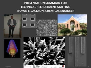
  • 1. PRESENTATION SUMMARY FOR TECHNICAL RECRUITMENT STAFFINGSHAWN E. JACKSON, CHEMICAL ENGINEER 1/17/2011 1
  • 2. CAREER SUMMARY A recognized successful mid-level engineering and clinical professional with professional background and education across several industries including petroleum, high technology integrated electronics, biotechnology, clinical healthcare, and nanotechnology. Career experiences in Process Engineering and Development, Process Improvement, Process Optimization and Control, Process Safety, Project Engineering, and Project Leadership and Supervision. Proven ability to bridge technology and business goals to provide productive solutions on time or prior to a business deadline. Demonstrated ability to implement technological solutions that harness applied scientific theory to solve a given problem. Experienced Team Builder with expertise in building Customer Relations across multi-disciplinary and cross functional teams, including multi-cultural Team Environments in international business organizations at the global level. Excellent communicator with proven technical writing and presentation skills. Quick learner that rapidly adapts to emerging technologies with the ability to change dynamically with business goals and objectives. 1/17/2011 2
  • 3. EDUCATION AND HONORS - ENGINEERING University of Arizona Bachelor of Science Degree in Chemical Engineering, Chemical Engineering 1994 – 1998 ● Baird and Honors Scholarship Recipient ● Proficient with Chemical Engineering Process Simulation Software ● Chemical Engineering Software Problem Solving Applications for Unit Operations ● Chemical Engineering Unit Operations and Science ● Hazardous Waste Treatment Unit Operations ● Chemical and Analytical Laboratory Methods ● FORTRAN Programming, Visual Basic, BASIC ● Operating Systems, Software Applications Arizona State University N/A, Electrical Engineering 1997 – 1999 ● Started Program Requirements for a Master of Science Degree In Electrical Engineering with an Emphasis In Solid State Electronics ● Completed courses in Semiconductor Processing and Device Theory Motorola University - Corporate Training Institute N/A, Corporate Manufacturing and Leadership Training 1997 – 1999 Corporate Training Courses:● Manufacturing Excellence and (Quality) Improvement● Six Sigma Quality Training● JMP Statistical Analysis Software for DOE, Data Analysis and Six Sigma Applications● Design of Experiments (DOE)● Process Capability● Measurement Capability, Gage R&R Studies● Leadership Training – Steven Covey: 7 Habits of Highly Effective People; Dale Carnegie; Dennis Deaton 1/17/2011 3
  • 4. CAREER CONTRIBUTIONS AND ACHIEVEMENTS ● Manufacturing Excellence Awards ● Engineering Project Management ● Engineering Project Supervision ● Process Developments ● Process Implementations ● Process Improvements ● Applied Engineering Methods ● Process Characterization ● Quality Initiatives and Implementation ● Continuous Improvement Initiatives ● Quality Standards Compliance ● Direct Contributions in IC Manufacturing Success ● Reliability of Scientific and Clinical Results ● Proven Leadership Success ● Team Building for Success ● Engineering Technical Publication ● Technical Process Change Approvals ● Technical Writing and Presentations ● Communication Skills ● Continuous Education and Excellence ● Exceptional Performance Reviews ● Exceptional Salary History Record ● Cost Savings ● Philanthropic Activities 1/17/2011 4
  • 5. PROFESSIONAL DEVELOPMENT AND LEADERSHIP TRAINING International Leadership Role in a High Technology Company for Next Generation IC Technologies Leadership Training – Steven Covey: 7 Habits of Highly Effective People; Dale Carnegie; Dennis Deaton Manufacturing Excellence and Statistical Process Control Methods Management Quality Standards for Continuous Improvement: Six Sigma, ISO9000, ISO9001 American Institute of Chemical Engineers 1/17/2011 5
  • 6. ADDITIONAL COMPETENCIES ● Manufacturing Process Monitoring and Control Software ● JMP Statistical Analysis Software Applications ● FORTRAN Programming, Visual Basic, BASIC ● Computer Literacy in All Respects ● Operating System and Database Management Experience ● Specialized Experience in Semiconductor Process Equipment and External Interface Systems for complete designed and built Integrated Circuits ● Specialized Experience in Semiconductor Analytical Methods and Metrology Process and External Interface Systems for Process Characterization ● Proficient with Chemical Engineering Process Simulation Software ● Chemical Engineering Software Problem Solving Applications for Unit Operations ● Semiconductor Process Modeling Software ● Electrocardiography Monitoring and Interpretation ● Medical Laboratory and Patient Care Experience ● Chemical Engineering Unit Operations and Science ● Hazardous Waste Treatment Unit Operations ● Chemical, Analytical and Medical Laboratory Methods ●Material and Spectroscopy Analysis Techniques ● Conversational Japanese, French and Spanish 1/17/2011 6
  • 7. DIRECT EXPERIENCE IN CHEMICAL ENGINEERING & PROFESSSIONAL WORKS DIRECT EXPERIENCE IN CHEMICAL ENGINEERING & PROFESSSIONAL WORKS ● Bachelor of Science Degree in Chemical Engineering with 8 years of Applied Chemical Engineering Experience. 12 years of experience and education with emphasis in chemical engineering applications. ● Industry experience: Semiconductor Manufacturing Process and Development; Nanotechnology Research and Development; Industrial Waste Treatment and Municipal Waste Treatment; Regulatory Standards: OSHA, EPA, ADEQ and Phoenix City Code for Safety Standards, Semiconductor Equipment and Materials International Standards, and ASTM Standards for Government Space and Military Testing Requirements. ● 6 years of Solid State Microelectronics Manufacturing and Process Development Experience. ● Specific and direct experiences in engineering problem solving and problem resolutions in process technologies and modules of integrated circuit manufacture with most notable experiences CVD processes; CVD, Diffusion, Implantation and Photolithography Metrology; Defectivity, Yield Enhancement, and Inspection Technologies; Diffusion Process; Implantation Process and Electrical Device Parametrics; Rapid Thermal Processing; Photolithography Process; Wet Process Engineering; Wafer Surface Cleaning and Chemical Mechanical Polish Process Technologies; and Single Crystal Growth Czochralski (CZ) Processes. GaAs and Si device process, manufacturing and process development experiences. ● Medical Laboratory experience in Microbiology, Chemistry, Hematology, Urinalysis, Coagulation, and Blood Bank. 5 years experience and education with Clinical Solutions, Diagnostic Equipment, Technology and In-Vitro Diagnostics methods and applications. ● 7 years of Project Engineering and Process Engineering responsibilities, with long term success track record in providing deliverables and meeting business goals prior to or on time to a given deadline. ● National and International Travel experience (up to 75%) with global leaders in the microelectronics industry in an Applications Engineering role. ● Professional References and further specific details related to professional experiences available upon request and over http://www.LinkedIn.com/in/shawnejackson. 1/17/2011 7
  • 8. CAREER HISTORY WITH MAJOR ACCOMPLISHMENTS - Nanotechnology 2008 – 2009; Materials and Electrochemical Research (MER) Corporation; Tucson, AZResearch Engineer with the Nanotechnology / Advanced Composite Materials Group ● Maintained the continuous chemical vapor deposition reactors for nanotube production processing and films deposition for advanced composites research and development applications; including process characterization, improvement and optimization, safety, process monitoring and control via Labview Software Process Control applications, process analysis and sample preparation for material, optical and electrical spectroscopy research methods, and input for design improvements. Improved chemical delivery of precursors to process reactors and reaction kinetics via process and reactor upgrades to include modifications to automated process control of syringe pumps, upgrades to HPLC pumps; design improvements to liquid reactant input piping and thermal control process; and liquid and vapor phase catalysis control with reactor column input design improvements. ● Acquired experience in research and production Chemical Vapor Deposition (CVD) thin film processes for double wall (DWNTs), single wall (SWNTs), multi-wall carbon nanotubes (MWCNTs) and SiC-CVD deposited films for advanced composite material applications and development projects for the United States Department of Defense and NASA Space System Projects. Strengthened experience in materials, optical and electrical spectroscopy analysis methods via Thermogravimetric Analysis (TGA), Scanning Electron Microscopy (SEM), Energy Dispersive X-Ray Spectroscopy (EDS), Near-IR Spectroscopy (N-IR) and research methods for material characterization with Raman Spectroscopy (Raman) and Tunneling Electron Microscopy (TEM). ● Achieved a process improvement of 425% with respect to continuous process reactor up-time. Determined root causes of defective chemical vapor deposited nanotube films and optimum thin film growth rates per time and reactant input concentration. Engineered corrective actions to prevent reoccurrence of defective thin film properties and to ensure constancy in film electrical and material characteristics for advanced development applications and to deliver thin film material orders to United States Department of Defense customers on schedule. ● Generated a process mass balance coincident with the process monitoring database to quantify and track efficiency of the reaction kinetics and thermodynamic conversion of reactants input to system to achieve desired products. Analyzed gas phase products via Mass Spectroscopy in-situ methods, and solid phase products via TGA and SEM methods. ● Enhanced Composite and Mechanical Strength Properties of Advanced C-Fiber Composites by over 40% via experimentation and generation of process development methods for production of Nanotube Reinforced Resins, integrating and improving process steps for building Nanotube Reinforced Advanced Composites, and adhering to ASTM Standards for high technology United States Space and Military applications. ● Responsible for vendor relations and suppliers of reactor chemicals, reactor consumables, reactor parts, cost controls, process upgrade part specifications and design criteria, material specifications, research into design improvements to existing configurations while developing industry supplier relationships, while maintaining continuous reactor production requirements to filling customer orders and internal research requirements. 1/17/2011 8
  • 9. CAREER HISTORY WITH MAJOR ACCOMPLISHMENTS – Semiconductor Processing2000 – 2001; Accretech USA, Inc. or TSK America, Inc. – U.S. Division of Accretech or Tokyo Seimitsu Co. (TSK), LTD.; San Jose and Milpitas, CAApplications Engineer with Semiconductor Equipment Division, Applications Engineering Group ● Managed next generation Brightfield Patterned and Unpatterned Wafer Inspection Systems Yield Enhancement Applications, Equipment and Software System process integration, facilities installation, system calibration, and capability projects for high volume, high technology integrated circuit manufacturers throughout the United States and Worldwide locations (Micron Technology, Infineon Technologies, Texas Instruments, Intel corporation, Advanced Micro Devices – GlobalFoundries Inc., IBM, NEC, Toshiba, and others). Bridged technology and business goals to provide productive manufacturing engineered yield improvements and cost savings with reduction in defect density across manufactured device technologies. Applied engineering applications approaches to detect defect densities on the order of greater than 100% of previous detection methods at critical process steps with the potential net effect of reducing cost for yield loss of next generation electrical device circuits with stricter tolerances and critical dimensions on the same order of magnitude. ● Performed Customer Demonstrations of Brightfield Inspection capabilities. Provided feedback and engineering evaluations related to overall process integration and system performance, theoretical and practical design strengths and limitations, and customer satisfaction to Worldwide Divisions of our parent company and the Customer including reports and presentations to Worldwide Semiconductor Industry Association (SIA) Manufacturers and Process Development Groups, our Equipment System Development Division, our Application Engineering Groups and Corporate Managers. ● Responsible for all competing wafer inspection technologies, industry developments, and application alternatives at current and next generation design rules and semiconductor process roadmap for technology innovation and integration of our equipment to device and yield engineering approaches to solving process development and manufacturing challenges. Acquired a strong background in KLA-Tencor and industry competing inspection and yield management systems and the worldwide manufacturing defect challenges. 1/17/2011 9
  • 10. CAREER HISTORY WITH MAJOR ACCOMPLISHMENTS – Semiconductor Processing2000 – 2001; Accretech USA, Inc. or TSK America, Inc. – U.S. Division of Accretech or Tokyo Seimitsu Co. (TSK), LTD.; San Jose and Milpitas, CAApplications Engineer with Semiconductor Equipment Division, Applications Engineering Group ● Applications experience with the following defectivity-inspection equipment and yield management systems: -Win-Win50 Confocal Brightfield Patterned and Unpatterned Wafer Inspection Systems (footprints for 150-200mm and 200-300mm platforms).-Win-Win50 on/off-line Auto Defect Classification (ADC).-JVC Scanning Electron Microscope (SEM) Review tools and Auto Defect Classification (SEM-ADC) System (200mm and 300mm platforms). -Wafer Inspection Systems: KLA-Tencor Surfscan SP and SP2 series. -Yield Management Systems: KLA-Tencor Klarity Bitmap, Klarity Defect, ACE XP, Spatial Signature Analysis (SSA). ● Familiarity and up to working knowledge (experience) of application and use of these competing technologies for direct defect inspection capability evaluations and process specific applications for defect reduction in manufactured integrated circuits: -Brightfield Patterned Wafer Inspection Systems: KLA-Tencor Stealth (23XX series, 28XX series currently). -Darkfield Patterned Wafer Inspection Systems: KLA-Tencor AIT XP (Puma 91XX and 9500 series currently). ● Characterized complete system capabilities, documented results and wrote technical reports and documentation related to system capability and input into Equipment Manuals for Operation, Calibration, Maintenance and Facilities Integration of our Defect Inspection Technology Equipment for internal and customer training purposes. Provided technical input and training for Applications Engineering and Technical Staffing. Interviewed potential candidates for technical staff placement up to the Applications Engineering level and provided input into hiring decisions for our U.S. Division. ● National and International Travel experience (up to 75%) with global leaders in the microelectronics industry in this Applications Engineering role. Lived abroad in Tokyo, Japan performing work for global Semiconductor Industry Association (SIA) Customers and Tokyo Seimitsu Co. (TSK) Japan, LTD., TSK Micro Technologies Co., LTD. (MTC – a subsidiary of TSK) and in Dresden, Germany for Tokyo Seimitsu Co. (TSK) Europe, GmbH. 1/17/2011 10
  • 11. CAREER HISTORY WITH MAJOR ACCOMPLISHMENTS – Semiconductor Processing 1996–1999; Process Engineer at Freescale Semiconductor or Motorola, Inc., Semiconductor Products Sector Process Engineer with the Chemical Vapor Deposition Engineering Group ● In the Chemical Vapor Deposition Process Engineering Group, responsible for manufacturing sustaining support and off shift leadership support of technical personal with responsibilities to preventing product losses, deviations from safety standards, keeping equipment and processes running continuously while minimizing down time and maximizing wafer throughput, ensuring staff members understand and follow specifications and standard operating procedures, and discovery of engineering opportunities for process improvements and innovation. In addition, apply knowledge of engineering principles, theory and applied statistical methods to daily and long term success of product improvement initiatives and sustainment. Directly responsible for all dielectric, chemical vapor deposited films processes; dielectric, chemical vapor deposition films metrology; and film thickness metrology process requirements for off shift manufacturing, while applying corrective actions to out of control process excursions. ● Chemical Vapor Deposition Equipment and Process Experience: -Applied Materials Producer PECVD, SACVD; Dielectric Deposition: USG (TEOS) Processes, PSG Process.-Watkins Johnson APCVD; Dielectric Deposition: BPSG Process, TEOS gap fill Process.-Film Thickness Metrology: Prometrix series; Doping Concentration Metrology: Rigaku XRF; Film Stress Metrology. 1/17/2011 11
  • 12. CAREER HISTORY WITH MAJOR ACCOMPLISHMENTS – Semiconductor Processing 1996–1999; Process Engineer at Freescale Semiconductor or Motorola, Inc., Semiconductor Products SectorProcess Engineer with the Diffusion Process Engineering Group ● In the Diffusion Process Engineering Group, responsible for a process characterization and technology transfer project that included evaluation of optical and electrical properties of gate dielectric properties for non-volatile flash memory (NVM-Flash) process integration. Characterized the optical and electrical properties of an oxide/nitride/oxide (ONO) film stack for modified, high K dielectric constant process with a Keithley Instruments – Quantox, Non-Contact Gate Oxide Monitoring System, and Rudolph Ellipsometers, including defining diffusion processes for Gate Oxide Diffusion and Low Pressure Chemical Vapor Deposition (LPCVD) Nitride on Silicon Valley Group (SVG) Furnaces and Reactors. Further evaluation of the process included film etch rate, analytical methods of Secondary Ion Mass Spectroscopy (SIMs) and Tunneling Electron Microscopy (TEM) to show high K film qualities at oxide/nitride/oxide interfaces and to determine the top oxide diffusion “punch-through” characteristics of the ONO process. ● Diffusion Equipment and Process Experience:-Silicon Valley Group (formerly a subsidiary of ASM Lithography Holding N.V.) Diffusion Furnaces; Gate Oxide Diffusion Processes, LPCVD Process. -Rudolph Technologies, Ellipsometers ; Keithley Instruments, Quantox Non-Contact Gate Oxide Monitoring System. 1/17/2011 12
  • 13. CAREER HISTORY WITH MAJOR ACCOMPLISHMENTS – Semiconductor Processing 1996–1999; Process Engineer at Freescale Semiconductor or Motorola, Inc., Semiconductor Products SectorProcess Engineer with the Yield Enhancement Engineering Group ● In the Defectivity and Yield Enhancement Process Engineering Group, responsible for root cause analysis and determination of process deviations and process changes for device yield improvement and cost savings. Recommendations and process change board approvals led to defect reduction of 30% within the double poly capacitor process module and cost savings of over $100K annually. Received a Manufacturing Excellence Award for project contributions from Motorola Semiconductor Products and Services Group. ● Defectivity and Yield Management Process Equipment Experience: - KLA-Tencor Defectivity and Inspection Systems (3200 series, Brightfield Inspection Technology); KLA-Tencor Defect Review Station (2540 series). - Furthered experience with Photolithography (Cannon i4 and Nikon), Etch (Teagal), Wafer Cleans and Brush Scrub Process Equipment with respect to defectivity excursions at current design rules and equipment configurations specific to process designed criteria. 1/17/2011 13
  • 14. CAREER HISTORY WITH MAJOR ACCOMPLISHMENTS – Semiconductor Processing 1996–1999; Process Engineer at Freescale Semiconductor or Motorola, Inc., Semiconductor Products SectorProcess Engineer with the Implant Engineering Group ● In the Ion Implantation Process Engineering Group, responsible for and delivered, on time, the installation of two medium current implantation process technologies to increase current manufacturing throughput of compound semiconductor products by 150% for all production implant processes. Experienced with Ion Implant Equipment installation and safety standards. Responsible for setup, characterization and optimization of all the new generation ion implant and RTP process recipes; performed device analysis to determine dose and energy sensitivities of the ion implanter systems and temperature sensitivities of the rapid thermal process (RTP) systems for process integration and tool matching to existing ion implantation and RTP tool sets. ● Ion Implantation Equipment and Process Experience: - Eaton Corporation (Axcelis Technologies Inc.) 8250 and 6200 Medium Current Implantation process technologies including residual gas analyzer (RGA) process monitoring system equipment for ion implant species control during Be and H implantation processes. - Rapid Thermal Processing (RTP) equipment and process. Thermawave Implantation Metrology process. 1/17/2011 14
  • 15. CAREER HISTORY WITH MAJOR ACCOMPLISHMENTS – Semiconductor Processing 1996–1999; Process Engineer at Freescale Semiconductor or Motorola, Inc., Semiconductor Products Sector Process Engineer with the Photolithography Engineering Group ● In the Photolithography Process Engineering Group, completed manufacturing process development and equipment integration for scaled up manufacturing efforts. Responsible for measurement and process capability studies, quality improvement, statistical process control (SPC) and process control for several process engineering improvements. Investigated critical dimension (CD) and Overlay control methods and technology and was responsible for a complete equipment upgrade, transfer and installation of an optical CD and Overlay tool, including complete release of all process recipes at after develop inspect (ADI) and after cleans inspect (ACI, post etch), complete training of all factory staffing and completion of all technical specifications for operation, troubleshooting, and procedures for process control. Developed a dual polymer, Bilayer liftoff process at the gate layer with the photolithography and device development groups. Responsible for all photolithography equipment process developments, including evaluation of films, thickness requirements, exposure relationships, and develop processes. Co-authored a technical publication in Motorola Proceedings for the latter process and presented findings at the Annual Motorola Technical Enrichment Matrix. ● Photolithography Equipment and Process Experience: - Vapor Prime Process Equipment, Silicon Valley Group 8600 Coater and 8600 Developer Tracks, Prometrix 7XXX series Film Thickness Metrology tools, BioRad Quaestar 1 and 5 CD and Overlay Metrology tools, Canon i4 and i1 Photolithography Steppers, Phillips Scanning Electron Microscope (SEM) and competing SEM technologies for process alternatives (Hitache and KLA CD-SEM technologies), Defectivity Inspection Microscopes, Analytical Lab Atomic Force Microscope (AFM) analysis techniques. 1/17/2011 15
  • 16. CAREER HISTORY WITH MAJOR ACCOMPLISHMENTS – Semiconductor Processing 1996–1999; Process Engineer at Freescale Semiconductor or Motorola, Inc., Semiconductor Products Sector Process Engineer with the Wet Chemical Process / Chemical Mechanical Polish Engineering Group ● In the Wet Chemical Process / Chemical Mechanical Polish Engineering Group, characterized starting Si substrate material (bare wafer) wet chemical cleaning and brush scrub process technologies for metal and particulate contamination levels, post chemical mechanical polish process, prior to shipment to all Motorola SPS factories. Developed and implemented a statistical process control monitoring system to control Si substrate quality and reliability metrics related to substrate metal and particulate contamination. Established SPC control charts, out of control action plans, process specifications and trained all sector staffing on proper control plan and new equipment integration plans for laser scanning inspection technologies. Established a database management system and programming solution to providing real time or daily process performance with respect to handling and manipulating large data sets for SPC and control applications. ● Wet Chemical Process / Chemical Mechanical Polish Equipment and Process Experience: - Bold Cleaning Technologies (automated, batch, wet chemical cleans process technologies) and previous generation wet process cleaning technologies, Wafer Brush Scrub Process technologies, KLA-Tencor Surfscan 6XXX series laser scattering inspection technologies, electrical grade resistivity inspection technologies, Analytical Laboratory Techniques and Equipment for Total X-Ray Flouresance (TXRF) analysis techniques. 1/17/2011 16
  • 17. CAREER HISTORY WITH MAJOR ACCOMPLISHMENTS – Semiconductor Processing1996; Texas Instruments, Inc. (now TriQuint Semiconductor); Dallas, TXProcess Engineer Co-op with the Wet Chemical Process Engineering Group in the Gallium Arsenide (GaAs) Operations Division of the Defense Systems and Electronics Group (DSEG) ● In the Wet Chemical Process Engineering Group, responsible for oversight and deliverables towards four process engineering manufacturing and development project initiatives while taking direction from the process engineering manager and senior process engineer staffing. Experimented and developed the batch process conditions and wet etch rates for an electrochemical plated metal removal chemistry. Experimented with environmentally safer wet etch chemicals via the Environmental Protection Agency (EPA) chemical replacement and reduction plan to remove toxic compound chemical solutions from mainstream semiconductor manufacturing methods, thereby reducing potential and real long term human exposure effects and environmental contamination concerns. Coincident with the former EPA Toxic Chemical Reduction and Replacement Plan for US manufacturers, determined de-ionized (DI) water factory usage related to wet chemical batch process technologies for reduction feasibility analysis. Finally, converted all process programs on a photoresist stripper to handle two different wafer diameters during standard compound semiconductor manufacturing process operations seamlessly. 1/17/2011 17
  • 18. CAREER HISTORY WITH MAJOR ACCOMPLISHMENTS – Clinical Medical and Laboratory2006 – 2008; Carondelet Health Network; Tucson, AZLaboratory Technical Assistant with the Clinical Laboratory; Patient Care Technician with the Medical Units at St. Mary’s and St. Joseph’s Hospitals ● Dedicated to the highest standards of quality and excellence in healthcare from a Clinical and Patient perspective. Conformed, without deviation or error, to clinical lab and patient care training procedures and protocols as outlined through corporate training and government regulatory standards such as the Joint Commission on the Accreditation of Health Care Organizations. Maximized turn around times of patient clinical test specimens while ensuring the reliability of test results. Meticulously followed scientific and clinical logic to prioritize objectives and specimen processing in a high volume clinical laboratory environment. ● Continuously experienced and educated in the clinical laboratory functional disciplines; including in depth experience in Microbiology, Hematology, Urinalysis, Coagulation, Chemistry and Blood Bank. Maintained these standards through continuous education in relevant degree related coursework, annual review of all specifications and procedures, knowledge based testing in the functional disciplines, continuous education and practice to maintain current with highest quality patient care interventions and procedures and applying problem solving strategies to daily work activities. ● Specialized in Patient Care Technician competencies in key medical units to be capable of assisting in every major medical unit of the hospital. Focused on Cardiac Medicine and Nursing science and procedures with additional knowledge based training and experiences primarily in the Medical Surgery, Rehabilitation and Orthopedic Units with assignments delegated from the Central Resource Staffing Team. Emphasized strong team building and professional relationships with colleagues across the cross functional disciplines within the Hospital Network. Fully capable of resuscitating victims of respiratory arrest, cardiac arrest, blocked airway and drowning. Competent in identifying and understanding dysrhythmic heart functions and the associated nursing interventions related to a given deviation from normal heart rhythmic functioning. 1/17/2011 18
  • 19. CAREER HISTORY WITH MAJOR ACCOMPLISHMENTS – Clinical Medical and Laboratory 2002 – 2006; Tucson Medical Center; Tucson, AZMicrobiology Laboratory Technical Assistant with the Microbiology Clinical Laboratory ● Acquired in depth experience with sample preparation and in-vitro diagnostics methods for Microbiology laboratory test specimens. Prepared quality control samples for microbiological pathogen growth and water quality standards testing. Resolved technical issues related to medical lab testing methods with the medical and clinical laboratory staff. Independently prioritized workflow and test sample preparation in a 700 bed hospital. ● Operation of microbiological equipment and instruments necessary to perform high-volume microbiological tests. Recognize equipment malfunction and follow corrective actions using established protocols to ensure patient test samples are not compromised. Monitored Microbiology Lab equipment and environment to ensure highest quality specimen integrity is constantly maintained through the growth and test cycles of the given specimen. Improved aerobic and anaerobic gas usage for cost savings on an order of 10% overall reduction in losses. 1/17/2011 19
  • 20. CAREER HISTORY WITH MAJOR ACCOMPLISHMENTS – Industrial and Municipal Hazardous Wastewater Treatment 1990-1991; Tri-Star, Inc.; Phoenix, AZProcess Engineering Intern with the Process Engineering Group ● Responsible for pre-industrial hazardous waste treatment processes in metal finishing and electroplating process operations, including treatment of complex metal salts and cyanide contaminated waste streams prior to safe effluent discharge to the municipal waste treatment plants. ● Maintained continuous and batch treatment chemical processes for cyanide destruction and metal salt reduction while recovering reusable metal wastes from the industrial processes via filter press and chemical flocculation processes. ● Performed batch tank recovery operations of metal finishing and electroplating baths to optimize process quality of finished products and adhere to Aerospace Industry and United States Military design specifications. ● Constant regulatory compliance achieved and improved upon by adhering to strict guidelines from the United States Occupational Safety and Health Administration (OSHA), the Environmental Protection Agency (EPA), Arizona Department of Environmental Quality (ADEQ), and Phoenix City Code for discharge to municipal waste streams. ● Certified by the State of Arizona for Grade One Wastewater Treatment Plant Operation. 1/17/2011 20
  • 21. PROFESSIONAL EMPLOYMENT HISTORY Relevant Chemical Engineering & Professional Experiences and Corporate Employers: ● 7/2008-Present; Seeking New Opportunities in Professional Endeavors and Employment; Experienced Research, Applications, and Process Engineer & Experienced Clinical Medical Professional. Experienced and/or knowledgeable in some areas of State and Federal Civil Legal Procedures. Seeking new opportunities in a corporate role with related technical responsibility to my background and experience sets. Seeking new business ventures or consulting opportunities. Pursued or pursuing several legal aspects of non-engineering related business matters that I must lead and close. .Industry: Research, Engineering, Technical and Legal Industries. ● 10/2008 – 9/2009; Materials and Electrochemical Research (MER) Corporation; Tucson, AZ; Research Engineer with the Nanotechnology / Advanced Composite Materials Group. Industry: Defense Systems and Aerospace Industry; U.S. Department of Defense, U.S. Space Systems (NASA), and Private Industry Corporations. ● 5/2006 – 7/2008; Carondelet Health Network; Tucson, AZ; Laboratory Technical Assistant with the Clinical Medical Laboratory Units; Patient Care Technician with the Patient Care Units in 2 hospitals. Industry: Clinical Medical, Biological Sciences and Healthcare. ●12/2002 – 8/2006; Tucson Medical Center; Tucson, AZ; Microbiology Laboratory Technologist Assistant with the Clinical Medical Microbiology Department in a 700 bed hospital. Industry: Clinical Medical, Biological Sciences and Healthcare. ● 1/2000 – 10/2001; Accretech USA, Inc. or TSK America, Inc. – U.S. Division of Tokyo Seimitsu Co. (TSK), LTD.; San Jose and Milpitas, CA; Applications Engineer with the Wafer Inspection Systems Division, Applications Engineering Group for 3 worldwide Divisions of the parent company: U.S. Division (Accretech USA), Accretech Japan and Accretech Europe. Industry: Semiconductor Integrated Electronics. ● 5/1996–9/1999; Freescale Semiconductor, Inc. or Motorola, Inc.; Phoenix, Tempe, Mesa and Chandler, AZ; Process Engineer with the Chemical Vapor Deposition, Diffusion, Yield Enhancement, Implantation, Photolithography, and Wet Chemical Process / Chemical Mechanical Polish Engineering Groups – Compound Semiconductor (GaAs) and Semiconductor (Si) Process Engineering Groups and experiences. Industry: Semiconductor Integrated Electronics. ● 1/1996-5/1996; Texas Instruments, Inc.; Dallas, TX; Process Engineer Co-op with the Wet Chemical Process Engineering Group in the Gallium Arsenide (GaAs) Operations Division of the Defense Systems and Electronics Group (DSEG). Industry: Semiconductor Integrated Electronics and U.S. Department of Defense Systems. ● 1/1995-12/1995; University of Arizona; Tucson, AZ; Research Assistant with the Electrical Engineering, Solid State Electronics Research Department, and the Environmentally Benign Semiconductor Processing Fab for the University of Arizona Engineering College. Industry: Research, Semiconductor Integrated Electronics and Environmental Engineering. ● 8/1990-12/1991; Tri-Star, Inc.; Phoenix, AZ; Process Engineering Intern with the Process Engineering Group with responsibilities in Metal Finishing and Electroplating Process and Industrial Hazardous Waste Treatment. Industry: Aerospace Industry and Environmental Engineering. 1/17/2011 21