2. CCD vs. CMOS
Row Drivers
Row Access
Clock &
Timing
Generation
Oscillator
Column Amps
Line
Driver
To Frame
Grabber
• Uniformity, the consistency of
response for different pixels under
identical illumination conditions.
Ideally, behavior would be uniform,
but spatial wafer processing variations, particulate defects and amplifier variations create nonuniformities. It is important to make a distinction between uniformity under
illumination and uniformity at or
near dark. CMOS imagers were traditionally much worse under both
regimes. Each pixel had an openloop output amplifier, and the offset
and gain of each amplifier varied considerably because of wafer processing variations, making both dark and
illuminated nonuniformities worse
than those in CCDs. Some people
predicted that this would defeat
CMOS imagers as device geometries
shrank and variances increased.
However, feedback-based amplifier structures can trade off gain for
greater uniformity under illumination. The amplifiers have made the illuminated uniformity of some CMOS
imagers closer to that of CCDs, sustainable as geometries shrink.
Still lacking, though, is offset variation of CMOS amplifiers, which
manifests itself as nonuniformity in
darkness. While CMOS imager man-
Gain
Analog-to-Digital
Conversion
ufacturers have invested considerable effort in suppressing dark
nonuniformity, it is still generally
worse than that of CCDs. This is a
significant issue in high-speed applications, where limited signal levels mean that dark nonuniformities
contribute significantly to overall
image degradation.
• Shuttering, the ability to start
and stop exposure arbitrarily. It is a
standard feature of virtually all consumer and most industrial CCDs,
especially interline transfer devices,
and is particularly important in machine vision applications. CCDs can
deliver superior electronic shuttering, with little fill-factor compromise,
even in small-pixel image sensors.
Implementing uniform electronic
shuttering in CMOS imagers requires
a number of transistors in each pixel.
In line-scan CMOS imagers, electronic shuttering does not compromise fill factor because shutter transistors can be placed adjacent to the
active area of each pixel. In areascan (matrix) imagers, uniform electronic shuttering comes at the expense of fill factor because the
opaque shutter transistors must be
placed in what would otherwise be
an optically sensitive area of each
Column Mux
Electron-to-Voltage
Conversion
Photon-to-Electron
Conversion
Complementary Metal Oxide Semiconductor
Image Sensor
Bias
Generation
Bias Decoupling
Connector
Camera
(Printed Circuit Board)
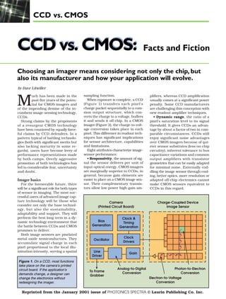
Figure 2. A CMOS imager converts
charge to voltage at the pixel, and
most functions are integrated into the
chip. This makes imager functions
less flexible but, for applications in
rugged environments, a CMOS
camera can be more reliable.
pixel. CMOS matrix sensor designers have dealt with this challenge in
two ways:
A nonuniform shutter, called a
rolling shutter, exposes different lines
of an array at different times. It reduces the number of in-pixel transistors, improving fill factor. This is
sometimes acceptable for consumer
imaging, but in higher-performance
applications, object motion manifests
as a distorted image.
A uniform synchronous shutter,
sometimes called a nonrolling shutter, exposes all pixels of the array at
the same time. Object motion stops
with no distortion, but this approach
consumes pixel area because it requires extra transistors in each pixel.
Users must choose between low fill
factor and small pixels on a small,
less-expensive image sensor, or large
pixels with much higher fill factor on
a larger, more costly image sensor.
• Speed, an area in which CMOS
arguably has the advantage over
CCDs because all camera functions
can be placed on the image sensor.
3. CCD vs. CMOS
With one die, signal and power
trace distances can be shorter,
with less inductance, capacitance
and propagation delays. To date,
though, CMOS imagers have established only modest advantages
in this regard, largely because of
early focus on consumer applications that do not demand notably high speeds compared with
the CCD’s industrial, scientific
and medical applications.
• Windowing. One unique capability of CMOS technology is
the ability to read out a portion of
the image sensor. This allows elevated frame or line rates for
small regions of interest. This is
an enabling capability for CMOS
imagers in some applications,
such as high-temporal-precision
object tracking in a subregion of
an image. CCDs generally have
limited abilities in windowing.
• Antiblooming, the ability to
gracefully drain localized overexposure without compromising the
rest of the image in the sensor.
CMOS generally has natural
blooming immunity. CCDs, on the
other hand, require specific engineering to achieve this capability. Many CCDs that have been
developed for consumer applications do, but those developed for
scientific applications generally do
not.
• Biasing and clocking. CMOS imagers have a clear edge in this regard. They generally operate with a
mizing leads and solder joints,
which are leading causes of circuit failures in extremely harsh
CMOS imagers offer superior integration,
environments.
power dissipation and system size at the
CMOS image sensors also
expense of image quality (particularly in
can be much more highly intelow light) and flexibility. They are the techgrated than CCD devices.
nology of choice for high-volume, spaceTiming generation, signal proconstrained applications where image
cessing, analog-to-digital conquality requirements are low. This makes
version, interface and other
them a natural fit for security cameras, PC
functions can all be put on the
videoconferencing, wireless handheld deimager chip. This means that
vice videoconferencing, bar-code scana CMOS-based camera can be
ners, fax machines, consumer scanners,
significantly smaller than a
toys, biometrics and some automotive incomparable CCD camera.
vehicle uses.
The user needs to consider,
CCDs offer superior image quality and
however, the cost of this inteflexibility at the expense of system size.
gration. CMOS imagers are
They remain the most suitable technolmanufactured in a wafer fabogy for high-end imaging applications,
rication process that must be
such as digital photography, broadcast
tailored for imaging perfortelevision, high-performance industrial
mance. These process adaptaimaging, and most scientific and medical
tions, compared with a nonapplications. Furthermore, flexibility
imaging mixed-signal process,
means users can achieve greater system
come with some penalties in
differentiation with CCDs than with CMOS
device scaling and power disimagers.
sipation. Although the pixel
Sustainable cost between the two techportion of the CMOS imager alnologies is approximately equal. This is
most invariably has lower
a major contradiction to the traditional
power dissipation than a CCD,
marketing pitch of virtually all of the solely
the power dissipation of other
CMOS imager companies.
circuits on the device can be
higher than that of a CCD
using companion chips from
optimized analog, digital and
mixed signal processes. At a system
single bias voltage and clock level.
level, this calls into question the noNonstandard biases are generated
tion that CMOS-based cameras have
on-chip with charge pump circuitry
lower power dissipation than CCDisolated from the user unless there is
based cameras. Often, CMOS is betsome noise leakage. CCDs typically
ter, but it is not unequivocally the
require a few higher -voltage
case, especially at high speeds (above
biases, but clocking has been simabout 25-MHz readout).
plified in modern devices that opThe other significant consideraerate with low-voltage clocks.
tions in system integration are adaptability, flexibility and speed of
Reliability
change. Most CMOS image sensors
Both image chip types are equally
are designed for a large, consumer
reliable in most consumer and inor near-consumer application. They
dustrial applications. In ultrarugged
are highly integrated and tailored for
environments, CMOS imagers have
one or a few applications. A system
an advantage because all circuit
designer should be careful not to infunctions can be placed on a sinvest fruitlessly in attempting to adapt
gle integrated circuit chip, minia highly application-specific device
for a use to which it is not suited.
Figure 3. Are they really stars? For an
CCD image sensors, on the other
ideal detector, each pixel’s response to
hand, are more general purpose. The
a photon would be identical, and the
pixel size and resolution are fixed in
“starlight” would be confined to the area
the device, but the user can easily
of the star.
tailor other aspects such as readout
Choose Your Imager
G
4. CCD vs. CMOS
tainability. Many CMOS startups are dedicated to high-volume applications. Pursuing
the highest-volume applications from a small base of
business has meant that
these companies have had to
price below their costs to win
business in commodity markets. Some start-ups will win
and sustain these prices.
Others will not and will have
to raise prices. Still others will
fail entirely.
CMOS users must be aware
of their suppliers’ profitability and cost structure to ensure that the technology will
be sustainable. The customer’s interest and the venture capitalist’s interest are
not well-aligned: Investors
want highest return, even if
that means highest risk,
whereas customers need stability because of the high cost
of midstream system design
change.
Increasingly, money and
talent are flowing to CMOS
Which costs less?
imaging,in large part because
One of the biggest misunderFigure 4. Shuttering is a concern in military target
of the high-volume applicastandings about image sensors
acquisition applications. A “rolling shutter” can start
tions enabled by the small
is cost.
and stop exposure on a CMOS device, but the
imaging devices and the high
Many early CMOS proponents
technique can result in a distorted image.
digital processing speeds. Over
argued that their technology
time, CMOS imagers should
would be vastly cheaper bebe able to advance into
cause it could be manufactured
higher-performance applications.
area. Both technologies offer appreon the same high-volume wafer proFor the moment, CCDs and CMOS
ciable volumes, but neither has such
cessing lines as mainstream logic
remain complementary technologies
commanding dominance over the
and memory devices. Had this as— one can do things uniquely that
other to establish untouchable
sumption proved out, CMOS would
the other cannot. Over time, this
economies of scale.
be cheaper than CCDs.
stark distinction will soften, with
CMOS may be less expensive at
However, the accommodations reCMOS imagers consuming more and
the system level than CCD, when
quired for good electro-optical permore of the CCD’s traditional appliconsidering the cost of related cirformance mean that CMOS imagers
cations. But this process will take
cuit functions such as timing genmust be made on specialty, lowerthe better part of a decade — at the
eration, biasing, analog signal provolume, optically adapted mixed-sigvery least.
cessing, digitization, interface and
nal processes and production lines.
feedback circuitry. But it is not
This means that CMOS and CCD
cheaper at a component level for the
image sensors do not have signifiMeet the author
pure image sensor function itself.
cantly different costs when produced
Dave Litwiller is Vice President,
The larger issue around pricing,
in similar volumes and with compaCorporate Marketing at DALSA in
Waterloo, Ontario, Canada.
particularly for CMOS users, is susrable cosmetic grading and silicon
speed, dynamic range, binning,
digitizing depth, nonlinear analog processing and other
customized modes of operation.
Even when it makes economic
sense to pay for sensor customization to suit an application, time to market can be an
issue. Because CMOS imagers
are systems on a chip, development time averages 18
months, depending on how
many circuit functions the designer can reuse from previous
designs in the same wafer fabrication process. And this
amount of time is growing because circuit complexity is outpacing design productivity. This
compares with about eight
months for new CCD designs in
established manufacturing
processes. CCD systems can
also be adapted with printed circuit board modifications,
whereas fully integrated CMOS
imaging systems require new
wafer runs.
G
DALSA is a leader in the design, development, manufacture, and sale of high-performance digital imaging
solutions. DALSA’s image sensor chip and electronic camera products are based on core competencies in
charge-coupled device (CCD) technology and CMOS imagers. DALSA sells to original equipment manufacturers (OEMs) requiring high performance imaging products for their vision systems. Our products are
high speed, high resolution and highly light sensitive. We serve markets in the United States, Europe, Japan
and Asia. For more information contact us at sales@dalsa.com or visit our web site at www.dalsa.com.