Photonic Materials
•Als PPT, PDF herunterladen•
30 gefällt mir•19,670 views

Slides on Photonic Materials.
![Photonics ,[object Object]](data:image/gif;base64,R0lGODlhAQABAIAAAAAAAP///yH5BAEAAAAALAAAAAABAAEAAAIBRAA7)
Empfohlen
Weitere ähnliche Inhalte
Was ist angesagt?
Was ist angesagt? (20)
Ähnlich wie Photonic Materials
Ähnlich wie Photonic Materials (20)
Mehr von Gaurav Singh Chandel
Kürzlich hochgeladen
Kürzlich hochgeladen (20)
Photonic Materials
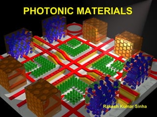
- 1. PHOTONIC MATERIALS Rakesh Kumar Sinha
- 4. Photonic Crystals Principles and Applications
- 6. Photonic crystal with a complete band gap when index contrast is large enough
- 8. In 2D photonic crystal structures it is possible to confine light within a cavity . Photonic band gaps appear in the plane of periodicity and in 2D we can achieve linear localization . By introducing a defect, i.e. removing one column, we may obtain a peak in the density of states localized in the photonic band gap – similar to semiconductors. The defect mode cannot penetrate the crystal in the xy-plane because of the band gap but extends in the z-direction
- 9. Photonic Crystals The Principle with photonic band gaps: “ optical insulators ” “ magical oven mitts” for holding and controlling light can trap light in cavities and waveguides (“wires”)
- 15. Properties of Photonic Crystals
- 16. Negative Refraction opposite of ordinary lens: only images close objects does not require curved lens can exceed classical diffraction limit
- 17. Properties of Photonic Crystals
- 18. Properties of Photonic Materials: Why no Scattering?? forbidden by gap (except for finite- crystal tunneling ) forbidden by Bloch ( k conserved)
- 19. Properties of Photonic Crystals
- 20. Properties of Photonic Crystals: Wide Angle Splitters
- 25. Self organized Nano Photonic Crystal Negative refraction in Photonic Crystal 3D IMAGING IN REAL SPACE Semiconductor substrate
- 26. Flat lens n = -1 d d = u + v v u object image Normal lens: Resolution cannot be greater than Flat lens : no limitation on the resolution Image resolution Normal lens
- 27. E H H E PIM PIM Turning light on its Head Positive Refraction PIM NIM E H E H Negative Refraction
- 28. Conventional Optical lens Photonic Crystal lens Advantages of Photonic Crystal lens Optical axis Limited aperture cannot NO Optical axis No limitation on aperture size Subwavelength imaging (evanescent wave amplification) PC : Scalability to sub-micron dimensions -> applications at optical frequencies
- 30. Applications Of Photonic Crystals Replacing conventional optical fibres The Glass Ceiling : Limits of Silica Loss : amplifiers every 50–100km … cannot use “exotic” wavelengths like 10.6µm Nonlinearities : after ~100km, cause dispersion, crosstalk, power limits (limited by mode area ~ single-mode, bending loss) also cannot be made (very) large for compact nonlinear devices Radical modifications to dispersion, polarization effects …tunability is limited Long Distances High Bit-Rates Dense Wavelength Multiplexing (DWDM) Compact Devices
- 32. Fabrication Of Photonic Crystals An example of a two-dimensional photonic crystal. The distance between the 200 nm wide pillars is about 500 nm and the pillars are 1500 nm long.
- 33. Fabrication Of Photonic Crystals Waveguide bend in a two-dimensional array of rods. The waveguide bend is defined by removing a row rods.
- 34. Fabrication Of Photonic Crystals Microfabrication : By layer by layer lithography. Colloidal self-assembly.
- 37. The Woodpile
- 41. 2µm Lithography at its best = 780nm resolution = 150nm 7µm (3 hours to make)
- 42. Lithography at its best 2µm ( 300nm diameter coils, suspended in ethanol, viscosity-damped )
- 43. Lithography at its best
- 44. Mass Production by Holographic Lithography absorptive material Four beams make 3d-periodic interference pattern (1.4µm) k -vector differences give reciprocal lattice vectors ( i.e. periodicity) beam polarizations + amplitudes (8 parameters) give unit cell
- 45. Holographic Lithography :The Results huge volumes , long-range periodic, fcc lattice…
- 46. Mass Production :Colloids microspheres (diameter < 1µm) silica (SiO 2 ) sediment by gravity into close-packed fcc lattice ! (evaporate)
- 47. Inverse Opals fcc solid spheres do not have a gap… … but fcc spherical holes in Si do have a gap [ figs courtesy D. Norris, UMN ] Infiltration sub-micron colloidal spheres Template (synthetic opal) 3D Remove Template “ Inverted Opal”
- 49. A Better Opal
- 56. THANK YOU !!!