SlideShare ist ein Scribd-Unternehmen logo
1 von 11
SEMICONDUCTOR MANUFACTURING - CLEAN ROOMS, WAFER
         CLEANING AND GETTERING- Chapter 4


           Year of Production              1998     2000     2002    2004     2007     2010     2013     2016     2018

     Technology Node (half pitch)         250 nm 180 nm     130 nm   90 nm    65 nm    45 nm    32 nm    22 nm    18 nm

       MPU Printed Gate Length                     100 nm   70 nm    53 nm    35 nm    25 nm    18 nm    13 nm    10 nm

      DRAM Bits/Chip (Sampling)           256M     512M      1G       4G      16G      32G      64G      128G     128G

      MPU Transistors/Chip (x106)                                     550     1100     2200     4400     8800     14,000

           Critical Defect Size           125 nm   90 nm    90 nm    90 nm    90 nm    90 nm    65 nm    45 nm    45 nm

     Starting Wafer Particles (cm-2 )                                <0.35    <0.18    <0.09    <0.09    <0.05    <0.05

   Starting Wafer Total Bulk Fe (cm-3 )   3x10¹⁰   1x10¹⁰   1x10¹⁰   1x10¹⁰   1x10¹⁰   1x10¹⁰   1x10¹⁰   1x10¹⁰   1x10¹⁰

     Metal Atoms on Wafer Surface         5x10⁹    1x10¹⁰   1x10¹⁰   1x10¹⁰   1x10¹⁰   1x10¹⁰   1x10¹⁰   1x10¹⁰   1x10¹⁰

          After Cleaning (cm-2 )

    Particles on Wafer Surface After                                  75       80       86       195      106      168

           Cleaning (#/wafer)
Three Tiered Approach

     Modern IC Factories Employ a Three Tiered Approach to
                 Controlling Unwanted Impurities
• 1. Clean Factories, Clean Room with Clean Environment:
  Air is Filtered, Machines Designed to Produce Minimum Particles,
  and Ultra Pure Chemicals and Gases Are used in Wafer
  Processing
• 2. Wafer Cleaning is Done Often and Thoroughly to
  Remove Particles and Contaminant Films on the Wafer Before
  They Get in to the Devices
• 3. Gettering: A Method by which unwanted impurities that
  get into wafer are pushed to non critical parts of wafer, typically
  wafer backside or wafer bulk, far away from active devices on the
  top wafer surface
• Contaminants may consist of
  particles, organic films (photoresist),
  heavy metals or alkali ions.
Level 1 Contamination Reduction: Clean Factories

                                                             • Particles may originate from
                                                               People, Machines, Chemicals, and
                                                               Process Gases
                                                             • Particles may be Airborne or
                                                               Suspended in Liquids and Gases
                                                             • Air Quality is Measured by the
                                                               “Class” of the Facility
                                                             • Class X Means in Cubic Foot of Air
                                                               There are Less Than X Total
                                                               Particles Greater than 0.5 um.
                                                             • Typical Office Bldg is Class 100,000
(Photo courtesy of Stanford Nanofabrication Facility.)


                                                         Factory environment is cleaned by:
                                                         • Hepa Filters and Recirculation for Air,
                                                         • “Bunny Suits” for Workers.
                                                         • Filtration of Chemicals and Gases.
                                                         • Manufacturing Protocols.
• In Clean Rooms Most Concern are 10 nm and 10 um Particles
• People Typically Emit Several Hundred Particles per Minute from
  Each cm2 Surface Area (5-10 million Particles per Minute per Person
  Typical). [Robots to Minimize Particle Generation]
• Bunny Suits to Cover Bodies and Clothing to Block Particle
  Emission
• Face Masks to Prevent Exhale of Particles
• Air Showers at Entrance
• Specially designed Machines to Minimize Particle generation
• Material Used Inside Clean Rooms are also Special
• Constant Air Filtration to Remove Particles as They are Generated
• Filtration of Chemicals to Minimize Particles coming from there
Level 2 Contamination Reduction: Wafer Cleaning


                             • RCA clean is “standard process”
                               used to remove organics, heavy
                               metals and alkali ions.

                             • Ultrasonic agitation is used to
                               dislodge particles.
Level 3 Contamination Reduction: Gettering
• Gettering is used to remove metal ions and alkali ions from device active regions.


   • For the alkali ions, gettering generally uses dielectric layers on the topside
     (PSG or barrier Si3N4 layers).
   • For metal ions, gettering generally uses traps on the wafer backside or in the
     wafer bulk.
   • Backside = extrinsic gettering. Bulk = intrinsic gettering.
PSG Layer
Devices in near
 surface region
Denuded Zone                          10 - 20 µm
 or Epi Layer


   Intrinsic
   Gettering
    Region                            500+ µ m


   Backside
   Gettering
    Region


• Heavy metal gettering relies on:
   • Metals diffusing very rapidly in silicon.
   • Metals segregating to “trap” sites.
SiO2 precipitates (white dots) in bulk
           of wafer.


• “Trap” sites can be created by SiO2 precipitates
  (intrinsic gettering), or by backside damage
  (extrinsic gettering).

• In intrinsic gettering, CZ silicon is used and SiO 2
   precipitates are formed in the wafer bulk through
   temperature cycling at the start of the process.
Modeling Particle Contamination and Yield


• ≈ 75% of yield loss in modern VLSI fabs is due to particle
contamination.

• Yield models depend on information
  about the distribution of particles.

• Particles on the order of 0.1 - 0.3 µm are
  the most troublesome:
     • larger particles precipitate easily
     • smaller ones coagulate into larger
       particles
Summary of Key Ideas
• A three-tiered approach is used to minimize contamination in wafer
  processing.

• Particle control, wafer cleaning and gettering are some of the "nuts and bolts"
  of chip manufacturing.

• The economic success (i.e. chip yields) of companies manufacturing chips
  today depends on careful attention to these issues.

• Level 1 control - clean factories through air filtration and highly purified
  chemicals and gases.

• Level 2 control - wafer cleaning using basic chemistry to remove unwanted
  elements from wafer surfaces.

• Level 3 control - gettering to collect metal atoms in regions of the wafer far
  away from active devices.

• Bottom line is chip yield. Since "bad" die are manufactured alongside "good"
  die, increasing yield leads to better profitability in manufacturing chips.

Weitere ähnliche Inhalte

Was ist angesagt? (20)

Device isolation
Device isolationDevice isolation
Device isolation
 
vlsi fabrication
vlsi fabricationvlsi fabrication
vlsi fabrication
 
Fabrication steps of IC
Fabrication steps of ICFabrication steps of IC
Fabrication steps of IC
 
Mos short channel effects
Mos short channel effectsMos short channel effects
Mos short channel effects
 
Cmos process flow
Cmos process flowCmos process flow
Cmos process flow
 
Wafer cutting
Wafer cuttingWafer cutting
Wafer cutting
 
Nmos design using synopsys TCAD tool
Nmos design using synopsys TCAD toolNmos design using synopsys TCAD tool
Nmos design using synopsys TCAD tool
 
Fabrication of IC
Fabrication of ICFabrication of IC
Fabrication of IC
 
Mosfet
MosfetMosfet
Mosfet
 
Electron beam lithography
Electron beam lithographyElectron beam lithography
Electron beam lithography
 
P1121110526
P1121110526P1121110526
P1121110526
 
Tunnel diode sunum
Tunnel diode sunumTunnel diode sunum
Tunnel diode sunum
 
integrated circuit febrication
integrated circuit febricationintegrated circuit febrication
integrated circuit febrication
 
The electron synchrotron
The electron synchrotronThe electron synchrotron
The electron synchrotron
 
SOI
SOISOI
SOI
 
MOSFETs (10EC63) Notes for Electronics & Communication Engineering Students o...
MOSFETs (10EC63) Notes for Electronics & Communication Engineering Students o...MOSFETs (10EC63) Notes for Electronics & Communication Engineering Students o...
MOSFETs (10EC63) Notes for Electronics & Communication Engineering Students o...
 
Klystron 1
Klystron 1Klystron 1
Klystron 1
 
Vlsi 2
Vlsi 2Vlsi 2
Vlsi 2
 
MESFET
MESFETMESFET
MESFET
 
Bjt
BjtBjt
Bjt
 

Ähnlich wie Ch04

CMOS Topic 2 -manufacturing_process
CMOS Topic 2 -manufacturing_processCMOS Topic 2 -manufacturing_process
CMOS Topic 2 -manufacturing_processIkhwan_Fakrudin
 
Processors Manufacturing Technology By Dr Islam Salama.pdf
Processors Manufacturing Technology By Dr Islam Salama.pdfProcessors Manufacturing Technology By Dr Islam Salama.pdf
Processors Manufacturing Technology By Dr Islam Salama.pdfDr-Islam Salama
 
Air pollution control units
Air pollution control unitsAir pollution control units
Air pollution control unitsManoj Mota
 
Equipment to control particulates part 2
Equipment to control particulates part 2Equipment to control particulates part 2
Equipment to control particulates part 2GARRE RAVI KUMAR
 
Non-traditional-machining.pdf
Non-traditional-machining.pdfNon-traditional-machining.pdf
Non-traditional-machining.pdfShiru6
 
photolithography_a
photolithography_aphotolithography_a
photolithography_aguestda8318
 
air and noise pollution environmental protection and control
air and noise pollution  environmental protection and controlair and noise pollution  environmental protection and control
air and noise pollution environmental protection and controlSJ BASHA
 
Magnetic Filtration Metallic Contaminants
Magnetic Filtration Metallic ContaminantsMagnetic Filtration Metallic Contaminants
Magnetic Filtration Metallic ContaminantsPeter Hiscock
 
Control of particulate contaminants
Control of particulate contaminantsControl of particulate contaminants
Control of particulate contaminantsASuhasini
 
Wafer processing-1.pptx
Wafer processing-1.pptxWafer processing-1.pptx
Wafer processing-1.pptxYasmeenEmad7
 
Ajm(Abrasive jet machining)
Ajm(Abrasive jet machining)Ajm(Abrasive jet machining)
Ajm(Abrasive jet machining)Samandeep Singh
 
Down stream Processing (Lecture 6)
Down stream Processing (Lecture 6)Down stream Processing (Lecture 6)
Down stream Processing (Lecture 6)Saira Fatima
 
Testing/Manufacture/Metal & sheet metal testing equipments
Testing/Manufacture/Metal & sheet metal testing equipmentsTesting/Manufacture/Metal & sheet metal testing equipments
Testing/Manufacture/Metal & sheet metal testing equipmentsfec2020
 

Ähnlich wie Ch04 (20)

CMOS Topic 2 -manufacturing_process
CMOS Topic 2 -manufacturing_processCMOS Topic 2 -manufacturing_process
CMOS Topic 2 -manufacturing_process
 
Wet and Dry Etching
Wet and Dry EtchingWet and Dry Etching
Wet and Dry Etching
 
Processors Manufacturing Technology By Dr Islam Salama.pdf
Processors Manufacturing Technology By Dr Islam Salama.pdfProcessors Manufacturing Technology By Dr Islam Salama.pdf
Processors Manufacturing Technology By Dr Islam Salama.pdf
 
Air pollution control units
Air pollution control unitsAir pollution control units
Air pollution control units
 
Equipment to control particulates part 2
Equipment to control particulates part 2Equipment to control particulates part 2
Equipment to control particulates part 2
 
Non-traditional-machining.pdf
Non-traditional-machining.pdfNon-traditional-machining.pdf
Non-traditional-machining.pdf
 
Intro to x ray
Intro to x rayIntro to x ray
Intro to x ray
 
photolithography_a
photolithography_aphotolithography_a
photolithography_a
 
2q
2q2q
2q
 
air and noise pollution environmental protection and control
air and noise pollution  environmental protection and controlair and noise pollution  environmental protection and control
air and noise pollution environmental protection and control
 
contamination control
contamination controlcontamination control
contamination control
 
Wafer cleaning
Wafer cleaningWafer cleaning
Wafer cleaning
 
mm_pract5.ppt
mm_pract5.pptmm_pract5.ppt
mm_pract5.ppt
 
Magnetic Filtration Metallic Contaminants
Magnetic Filtration Metallic ContaminantsMagnetic Filtration Metallic Contaminants
Magnetic Filtration Metallic Contaminants
 
Control of particulate contaminants
Control of particulate contaminantsControl of particulate contaminants
Control of particulate contaminants
 
Wafer processing-1.pptx
Wafer processing-1.pptxWafer processing-1.pptx
Wafer processing-1.pptx
 
Ajm(Abrasive jet machining)
Ajm(Abrasive jet machining)Ajm(Abrasive jet machining)
Ajm(Abrasive jet machining)
 
Down stream Processing (Lecture 6)
Down stream Processing (Lecture 6)Down stream Processing (Lecture 6)
Down stream Processing (Lecture 6)
 
Clean air experts
Clean air expertsClean air experts
Clean air experts
 
Testing/Manufacture/Metal & sheet metal testing equipments
Testing/Manufacture/Metal & sheet metal testing equipmentsTesting/Manufacture/Metal & sheet metal testing equipments
Testing/Manufacture/Metal & sheet metal testing equipments
 

Mehr von Faiza Saher

Lecture 1 wireless
Lecture 1 wirelessLecture 1 wireless
Lecture 1 wirelessFaiza Saher
 
Modern digital and analog communications systems by b p-lathi-solutions-manual
Modern digital and analog communications systems by b p-lathi-solutions-manualModern digital and analog communications systems by b p-lathi-solutions-manual
Modern digital and analog communications systems by b p-lathi-solutions-manualFaiza Saher
 
Fourier series 1
Fourier series 1Fourier series 1
Fourier series 1Faiza Saher
 

Mehr von Faiza Saher (7)

Lecture 05
Lecture 05Lecture 05
Lecture 05
 
Chapter3
Chapter3Chapter3
Chapter3
 
Lecture 1 wireless
Lecture 1 wirelessLecture 1 wireless
Lecture 1 wireless
 
Modern digital and analog communications systems by b p-lathi-solutions-manual
Modern digital and analog communications systems by b p-lathi-solutions-manualModern digital and analog communications systems by b p-lathi-solutions-manual
Modern digital and analog communications systems by b p-lathi-solutions-manual
 
1010n3a
1010n3a1010n3a
1010n3a
 
Fourier series 1
Fourier series 1Fourier series 1
Fourier series 1
 
Fourier series
Fourier seriesFourier series
Fourier series
 

Kürzlich hochgeladen

Field Attribute Index Feature in Odoo 17
Field Attribute Index Feature in Odoo 17Field Attribute Index Feature in Odoo 17
Field Attribute Index Feature in Odoo 17Celine George
 
Solving Puzzles Benefits Everyone (English).pptx
Solving Puzzles Benefits Everyone (English).pptxSolving Puzzles Benefits Everyone (English).pptx
Solving Puzzles Benefits Everyone (English).pptxOH TEIK BIN
 
Introduction to ArtificiaI Intelligence in Higher Education
Introduction to ArtificiaI Intelligence in Higher EducationIntroduction to ArtificiaI Intelligence in Higher Education
Introduction to ArtificiaI Intelligence in Higher Educationpboyjonauth
 
Romantic Opera MUSIC FOR GRADE NINE pptx
Romantic Opera MUSIC FOR GRADE NINE pptxRomantic Opera MUSIC FOR GRADE NINE pptx
Romantic Opera MUSIC FOR GRADE NINE pptxsqpmdrvczh
 
Procuring digital preservation CAN be quick and painless with our new dynamic...
Procuring digital preservation CAN be quick and painless with our new dynamic...Procuring digital preservation CAN be quick and painless with our new dynamic...
Procuring digital preservation CAN be quick and painless with our new dynamic...Jisc
 
AmericanHighSchoolsprezentacijaoskolama.
AmericanHighSchoolsprezentacijaoskolama.AmericanHighSchoolsprezentacijaoskolama.
AmericanHighSchoolsprezentacijaoskolama.arsicmarija21
 
Keynote by Prof. Wurzer at Nordex about IP-design
Keynote by Prof. Wurzer at Nordex about IP-designKeynote by Prof. Wurzer at Nordex about IP-design
Keynote by Prof. Wurzer at Nordex about IP-designMIPLM
 
Types of Journalistic Writing Grade 8.pptx
Types of Journalistic Writing Grade 8.pptxTypes of Journalistic Writing Grade 8.pptx
Types of Journalistic Writing Grade 8.pptxEyham Joco
 
call girls in Kamla Market (DELHI) 🔝 >༒9953330565🔝 genuine Escort Service 🔝✔️✔️
call girls in Kamla Market (DELHI) 🔝 >༒9953330565🔝 genuine Escort Service 🔝✔️✔️call girls in Kamla Market (DELHI) 🔝 >༒9953330565🔝 genuine Escort Service 🔝✔️✔️
call girls in Kamla Market (DELHI) 🔝 >༒9953330565🔝 genuine Escort Service 🔝✔️✔️9953056974 Low Rate Call Girls In Saket, Delhi NCR
 
Framing an Appropriate Research Question 6b9b26d93da94caf993c038d9efcdedb.pdf
Framing an Appropriate Research Question 6b9b26d93da94caf993c038d9efcdedb.pdfFraming an Appropriate Research Question 6b9b26d93da94caf993c038d9efcdedb.pdf
Framing an Appropriate Research Question 6b9b26d93da94caf993c038d9efcdedb.pdfUjwalaBharambe
 
Roles & Responsibilities in Pharmacovigilance
Roles & Responsibilities in PharmacovigilanceRoles & Responsibilities in Pharmacovigilance
Roles & Responsibilities in PharmacovigilanceSamikshaHamane
 
Quarter 4 Peace-education.pptx Catch Up Friday
Quarter 4 Peace-education.pptx Catch Up FridayQuarter 4 Peace-education.pptx Catch Up Friday
Quarter 4 Peace-education.pptx Catch Up FridayMakMakNepo
 
How to do quick user assign in kanban in Odoo 17 ERP
How to do quick user assign in kanban in Odoo 17 ERPHow to do quick user assign in kanban in Odoo 17 ERP
How to do quick user assign in kanban in Odoo 17 ERPCeline George
 
ECONOMIC CONTEXT - PAPER 1 Q3: NEWSPAPERS.pptx
ECONOMIC CONTEXT - PAPER 1 Q3: NEWSPAPERS.pptxECONOMIC CONTEXT - PAPER 1 Q3: NEWSPAPERS.pptx
ECONOMIC CONTEXT - PAPER 1 Q3: NEWSPAPERS.pptxiammrhaywood
 
Earth Day Presentation wow hello nice great
Earth Day Presentation wow hello nice greatEarth Day Presentation wow hello nice great
Earth Day Presentation wow hello nice greatYousafMalik24
 
AMERICAN LANGUAGE HUB_Level2_Student'sBook_Answerkey.pdf
AMERICAN LANGUAGE HUB_Level2_Student'sBook_Answerkey.pdfAMERICAN LANGUAGE HUB_Level2_Student'sBook_Answerkey.pdf
AMERICAN LANGUAGE HUB_Level2_Student'sBook_Answerkey.pdfphamnguyenenglishnb
 
ENGLISH6-Q4-W3.pptxqurter our high choom
ENGLISH6-Q4-W3.pptxqurter our high choomENGLISH6-Q4-W3.pptxqurter our high choom
ENGLISH6-Q4-W3.pptxqurter our high choomnelietumpap1
 

Kürzlich hochgeladen (20)

Field Attribute Index Feature in Odoo 17
Field Attribute Index Feature in Odoo 17Field Attribute Index Feature in Odoo 17
Field Attribute Index Feature in Odoo 17
 
Solving Puzzles Benefits Everyone (English).pptx
Solving Puzzles Benefits Everyone (English).pptxSolving Puzzles Benefits Everyone (English).pptx
Solving Puzzles Benefits Everyone (English).pptx
 
Introduction to ArtificiaI Intelligence in Higher Education
Introduction to ArtificiaI Intelligence in Higher EducationIntroduction to ArtificiaI Intelligence in Higher Education
Introduction to ArtificiaI Intelligence in Higher Education
 
OS-operating systems- ch04 (Threads) ...
OS-operating systems- ch04 (Threads) ...OS-operating systems- ch04 (Threads) ...
OS-operating systems- ch04 (Threads) ...
 
Romantic Opera MUSIC FOR GRADE NINE pptx
Romantic Opera MUSIC FOR GRADE NINE pptxRomantic Opera MUSIC FOR GRADE NINE pptx
Romantic Opera MUSIC FOR GRADE NINE pptx
 
Procuring digital preservation CAN be quick and painless with our new dynamic...
Procuring digital preservation CAN be quick and painless with our new dynamic...Procuring digital preservation CAN be quick and painless with our new dynamic...
Procuring digital preservation CAN be quick and painless with our new dynamic...
 
TataKelola dan KamSiber Kecerdasan Buatan v022.pdf
TataKelola dan KamSiber Kecerdasan Buatan v022.pdfTataKelola dan KamSiber Kecerdasan Buatan v022.pdf
TataKelola dan KamSiber Kecerdasan Buatan v022.pdf
 
AmericanHighSchoolsprezentacijaoskolama.
AmericanHighSchoolsprezentacijaoskolama.AmericanHighSchoolsprezentacijaoskolama.
AmericanHighSchoolsprezentacijaoskolama.
 
Keynote by Prof. Wurzer at Nordex about IP-design
Keynote by Prof. Wurzer at Nordex about IP-designKeynote by Prof. Wurzer at Nordex about IP-design
Keynote by Prof. Wurzer at Nordex about IP-design
 
Types of Journalistic Writing Grade 8.pptx
Types of Journalistic Writing Grade 8.pptxTypes of Journalistic Writing Grade 8.pptx
Types of Journalistic Writing Grade 8.pptx
 
Model Call Girl in Tilak Nagar Delhi reach out to us at 🔝9953056974🔝
Model Call Girl in Tilak Nagar Delhi reach out to us at 🔝9953056974🔝Model Call Girl in Tilak Nagar Delhi reach out to us at 🔝9953056974🔝
Model Call Girl in Tilak Nagar Delhi reach out to us at 🔝9953056974🔝
 
call girls in Kamla Market (DELHI) 🔝 >༒9953330565🔝 genuine Escort Service 🔝✔️✔️
call girls in Kamla Market (DELHI) 🔝 >༒9953330565🔝 genuine Escort Service 🔝✔️✔️call girls in Kamla Market (DELHI) 🔝 >༒9953330565🔝 genuine Escort Service 🔝✔️✔️
call girls in Kamla Market (DELHI) 🔝 >༒9953330565🔝 genuine Escort Service 🔝✔️✔️
 
Framing an Appropriate Research Question 6b9b26d93da94caf993c038d9efcdedb.pdf
Framing an Appropriate Research Question 6b9b26d93da94caf993c038d9efcdedb.pdfFraming an Appropriate Research Question 6b9b26d93da94caf993c038d9efcdedb.pdf
Framing an Appropriate Research Question 6b9b26d93da94caf993c038d9efcdedb.pdf
 
Roles & Responsibilities in Pharmacovigilance
Roles & Responsibilities in PharmacovigilanceRoles & Responsibilities in Pharmacovigilance
Roles & Responsibilities in Pharmacovigilance
 
Quarter 4 Peace-education.pptx Catch Up Friday
Quarter 4 Peace-education.pptx Catch Up FridayQuarter 4 Peace-education.pptx Catch Up Friday
Quarter 4 Peace-education.pptx Catch Up Friday
 
How to do quick user assign in kanban in Odoo 17 ERP
How to do quick user assign in kanban in Odoo 17 ERPHow to do quick user assign in kanban in Odoo 17 ERP
How to do quick user assign in kanban in Odoo 17 ERP
 
ECONOMIC CONTEXT - PAPER 1 Q3: NEWSPAPERS.pptx
ECONOMIC CONTEXT - PAPER 1 Q3: NEWSPAPERS.pptxECONOMIC CONTEXT - PAPER 1 Q3: NEWSPAPERS.pptx
ECONOMIC CONTEXT - PAPER 1 Q3: NEWSPAPERS.pptx
 
Earth Day Presentation wow hello nice great
Earth Day Presentation wow hello nice greatEarth Day Presentation wow hello nice great
Earth Day Presentation wow hello nice great
 
AMERICAN LANGUAGE HUB_Level2_Student'sBook_Answerkey.pdf
AMERICAN LANGUAGE HUB_Level2_Student'sBook_Answerkey.pdfAMERICAN LANGUAGE HUB_Level2_Student'sBook_Answerkey.pdf
AMERICAN LANGUAGE HUB_Level2_Student'sBook_Answerkey.pdf
 
ENGLISH6-Q4-W3.pptxqurter our high choom
ENGLISH6-Q4-W3.pptxqurter our high choomENGLISH6-Q4-W3.pptxqurter our high choom
ENGLISH6-Q4-W3.pptxqurter our high choom
 

Ch04

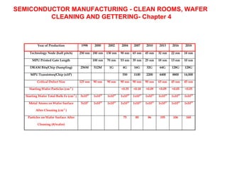
  • 1. SEMICONDUCTOR MANUFACTURING - CLEAN ROOMS, WAFER CLEANING AND GETTERING- Chapter 4 Year of Production 1998 2000 2002 2004 2007 2010 2013 2016 2018 Technology Node (half pitch) 250 nm 180 nm 130 nm 90 nm 65 nm 45 nm 32 nm 22 nm 18 nm MPU Printed Gate Length 100 nm 70 nm 53 nm 35 nm 25 nm 18 nm 13 nm 10 nm DRAM Bits/Chip (Sampling) 256M 512M 1G 4G 16G 32G 64G 128G 128G MPU Transistors/Chip (x106) 550 1100 2200 4400 8800 14,000 Critical Defect Size 125 nm 90 nm 90 nm 90 nm 90 nm 90 nm 65 nm 45 nm 45 nm Starting Wafer Particles (cm-2 ) <0.35 <0.18 <0.09 <0.09 <0.05 <0.05 Starting Wafer Total Bulk Fe (cm-3 ) 3x10¹⁰ 1x10¹⁰ 1x10¹⁰ 1x10¹⁰ 1x10¹⁰ 1x10¹⁰ 1x10¹⁰ 1x10¹⁰ 1x10¹⁰ Metal Atoms on Wafer Surface 5x10⁹ 1x10¹⁰ 1x10¹⁰ 1x10¹⁰ 1x10¹⁰ 1x10¹⁰ 1x10¹⁰ 1x10¹⁰ 1x10¹⁰ After Cleaning (cm-2 ) Particles on Wafer Surface After 75 80 86 195 106 168 Cleaning (#/wafer)
  • 2. Three Tiered Approach Modern IC Factories Employ a Three Tiered Approach to Controlling Unwanted Impurities • 1. Clean Factories, Clean Room with Clean Environment: Air is Filtered, Machines Designed to Produce Minimum Particles, and Ultra Pure Chemicals and Gases Are used in Wafer Processing • 2. Wafer Cleaning is Done Often and Thoroughly to Remove Particles and Contaminant Films on the Wafer Before They Get in to the Devices • 3. Gettering: A Method by which unwanted impurities that get into wafer are pushed to non critical parts of wafer, typically wafer backside or wafer bulk, far away from active devices on the top wafer surface
  • 3. • Contaminants may consist of particles, organic films (photoresist), heavy metals or alkali ions.
  • 4. Level 1 Contamination Reduction: Clean Factories • Particles may originate from People, Machines, Chemicals, and Process Gases • Particles may be Airborne or Suspended in Liquids and Gases • Air Quality is Measured by the “Class” of the Facility • Class X Means in Cubic Foot of Air There are Less Than X Total Particles Greater than 0.5 um. • Typical Office Bldg is Class 100,000 (Photo courtesy of Stanford Nanofabrication Facility.) Factory environment is cleaned by: • Hepa Filters and Recirculation for Air, • “Bunny Suits” for Workers. • Filtration of Chemicals and Gases. • Manufacturing Protocols.
  • 5. • In Clean Rooms Most Concern are 10 nm and 10 um Particles • People Typically Emit Several Hundred Particles per Minute from Each cm2 Surface Area (5-10 million Particles per Minute per Person Typical). [Robots to Minimize Particle Generation] • Bunny Suits to Cover Bodies and Clothing to Block Particle Emission • Face Masks to Prevent Exhale of Particles • Air Showers at Entrance • Specially designed Machines to Minimize Particle generation • Material Used Inside Clean Rooms are also Special • Constant Air Filtration to Remove Particles as They are Generated • Filtration of Chemicals to Minimize Particles coming from there
  • 6. Level 2 Contamination Reduction: Wafer Cleaning • RCA clean is “standard process” used to remove organics, heavy metals and alkali ions. • Ultrasonic agitation is used to dislodge particles.
  • 7. Level 3 Contamination Reduction: Gettering • Gettering is used to remove metal ions and alkali ions from device active regions. • For the alkali ions, gettering generally uses dielectric layers on the topside (PSG or barrier Si3N4 layers). • For metal ions, gettering generally uses traps on the wafer backside or in the wafer bulk. • Backside = extrinsic gettering. Bulk = intrinsic gettering.
  • 8. PSG Layer Devices in near surface region Denuded Zone 10 - 20 µm or Epi Layer Intrinsic Gettering Region 500+ µ m Backside Gettering Region • Heavy metal gettering relies on: • Metals diffusing very rapidly in silicon. • Metals segregating to “trap” sites.
  • 9. SiO2 precipitates (white dots) in bulk of wafer. • “Trap” sites can be created by SiO2 precipitates (intrinsic gettering), or by backside damage (extrinsic gettering). • In intrinsic gettering, CZ silicon is used and SiO 2 precipitates are formed in the wafer bulk through temperature cycling at the start of the process.
  • 10. Modeling Particle Contamination and Yield • ≈ 75% of yield loss in modern VLSI fabs is due to particle contamination. • Yield models depend on information about the distribution of particles. • Particles on the order of 0.1 - 0.3 µm are the most troublesome: • larger particles precipitate easily • smaller ones coagulate into larger particles
  • 11. Summary of Key Ideas • A three-tiered approach is used to minimize contamination in wafer processing. • Particle control, wafer cleaning and gettering are some of the "nuts and bolts" of chip manufacturing. • The economic success (i.e. chip yields) of companies manufacturing chips today depends on careful attention to these issues. • Level 1 control - clean factories through air filtration and highly purified chemicals and gases. • Level 2 control - wafer cleaning using basic chemistry to remove unwanted elements from wafer surfaces. • Level 3 control - gettering to collect metal atoms in regions of the wafer far away from active devices. • Bottom line is chip yield. Since "bad" die are manufactured alongside "good" die, increasing yield leads to better profitability in manufacturing chips.