SlideShare ist ein Scribd-Unternehmen logo
1 von 4
Downloaden Sie, um offline zu lesen
IJRET: International Journal of Research in Engineering and Technology eISSN: 2319-1163 | pISSN: 2321-7308
__________________________________________________________________________________________
Volume: 02 Issue: 10 | Oct-2013, Available @ http://www.ijret.org 573
COMPARISON OF LOGIC FAMILIES USING NAND GATE
Vibha Soni1
, Nitin Naiyar2
1, 2
Electronics & Telecommunication Engineering Department Rungta College of Engineering & Technology, Bhilai
490024, Chhattisgarh, India, vibhasoni178@rediffmail.com, naiyar16@gmail.com
Abstract
A digital circuit is constructed from small electronic circuits called logic gates that can be used to create combinational logic. A logic
gate is an idealized or physical device which implements a Boolean function. It is an arrangement of electrically controlled switches,
known as transistors. They are the fundamental building block for high performance data path circuits. The monolithic digital
integrated circuit devices can be constructed using several different designs methods which use different logic families. In this paper
different logic circuit families are compared. Power, delay and power-delay product are some of the performance parameters used for
comparison.
Keywords- CMOS, power, delay, power-delay product.
---------------------------------------------------------------------***-------------------------------------------------------------------------
1 INTRODUCTION
A logic gate performs a logical operation on one or more logic
inputs and produces a single logic output. Logic gates are
primarily implemented using diodes or transistors but can also
be constructed using electromagnetic relays, fluidic logic,
pneumatic logic, or even mechanical elements. In the present
work, NAND gate is implemented using RTL, DTL, TTL and
CMOS structures.
2 LOGIC FAMILIES
2.1 RTL
RTL stands for Resistor Transistor Logic. In RTL logic,
transistor is used in conjunction with resistors to create a logic
circuit. The NPN transistor used in RTL logic acts as an
inverter circuit. When high (Logic „1‟) input is applied at gate,
then transistor turns „ON‟ and low (logic 0‟) output is
obtained. The RTL NAND gate is shown in figure 1.
Fig. 1 RTL NAND gate
An RTL NAND gate circuit consists of two transistors Q1 and
Q2 connected as shown in figure 1. When both of input In1 or
In2 is driven high, corresponding transistor goes to saturation
and output is pulled to low value. When both the inputs In1
and In2 are driven low, corresponding transistor goes to OFF
state and output is pulled to high value.
2.2 DTL
DTL stands for Diode Transistor Logic. In DTL, the logic
function is implemented using diodes and transistors. Each of
the input is associated with one diode. Figure 2 shows DTL
NAND logic circuit. Here diode acts as „AND‟ circuit and is
IJRET: International Journal of Research in Engineering and Technology eISSN: 2319-1163 | pISSN: 2321-7308
__________________________________________________________________________________________
Volume: 02 Issue: 10 | Oct-2013, Available @ http://www.ijret.org 574
connected to a transistor inverter which acts as „NOT‟ circuit.
According to inputs going high value, the corresponding diode
conducts current, through the resistor. This turns „ON‟ the
transistor. The transistor act as short circuit and is grounded.
At the output, low value is obtained. If input In1 and In2 are
Low, the diodes do not conduct and thus output is at High
value.
Fig. 2 DTL NAND gate
2.3 TTL
TTL stands for Transistor-Transistor Logic. Figure 3 shows
the TTL NAND gate.
Fig. 3 TTL NAND gate
When one of the inputs is high, the output is high; otherwise,
the output is low. When both inputs In1 and In2 are high, the
two transistors on the left are in reverse active state. A current
flows through the resistor through the base and collector of
these transistors, and then through the base of the transistor on
the right, saturating it and bringing the output down near
ground When both inputs In1 and In2 are low, the easiest path
to ground through the resistor is through the base of the
transistors on the left to the inputs. This brings their collector
voltages low enough so that very little current can flow
through the base of the transistor on the right. This keeps that
transistor off, bringing the output to high. When only one of
the inputs is low, that input provides the easiest path to
ground, through its corresponding transistor. This keeps the
transistor on the right switched off.
2.4 CMOS
CMOS stands for complementary Metal Oxide
Semiconductor. It uses complementary arrangements of N-
channel and P-channel Field Effect Transistor. Since the initial
devices used oxide-isolated metal gates, they are called
CMOS. CMOS NAND gate is shown in figure 4.
Fig. 4 CMOS NAND gate
3 RESULTS & DISSCUSSION
The output waveforms are shown in figure 5. The x axis
shows the voltage level in volts and y axis shows time in
seconds. The input voltage level is given by V(in1) and
V(in2). The corresponding NAND logic output can be
observed from V(out). Thus it can be seen that if both of the
two inputs are at high logic level, the corresponding output
shows logic „1‟ and if both the inputs are low, then output is at
logic „1‟. Simulations have been performed for RTL, DTL,
IJRET: International Journal of Research in Engineering and Technology eISSN: 2319-1163 | pISSN: 2321-7308
__________________________________________________________________________________________
Volume: 02 Issue: 10 | Oct-2013, Available @ http://www.ijret.org 575
TTL and CMOS NAND logic. The output waveform shown in
fig 5 is of CMOS NAND logic.
Fig. 5 Output Waveforms
Table 1 shows the comparison between RTL, DTL, TTL and
CMOS logic families. The simulation had been carried out at
power supply voltage value of 3 V. Power, delay, and power-
delay products are few of the performance parameters
considered here for comparison between various logic
families.
Table 1 Comparison of different logic families
It can be observed from Table 1 that power dissipation in
CMOS logic is least as compared to all the logic families. The
power delay product which shows the figure of merit is least
for CMOS technology and hence CMOS logic family
outperforms all the logic families.
Figure 6 shows the graphical representation of power
consumption in different logic families. It can be seen that
TTL logic families consume highest power and minimum
power dissipation is in CMOS logic family.
Fig. 6 Power dissipation in various logic families
Figure 7 shows the graphical representation of delay in
different logic families. It is observed that DTL logic family
has the maximum delay compared to CMOS logic family.
Fig. 7 Delay in various logic families
Figure 8 shows the graphical representation of power- delay
product in different logic families. It can be seen that though
delay in CMOS is high than TTL, but power-delay product of
CMOS is minimum compared to other logic families. Thus
overall performance of CMOS logic family is better in
comparison with other logic families.
0.00E+00
5.00E-04
1.00E-03
1.50E-03
2.00E-03
2.50E-03
3.00E-03
3.50E-03
4.00E-03
Power
Power
0.00E+00
1.00E+01
2.00E+01
3.00E+01
4.00E+01
5.00E+01
6.00E+01
7.00E+01
8.00E+01
9.00E+01
Delay
Delay
IJRET: International Journal of Research in Engineering and Technology eISSN: 2319-1163 | pISSN: 2321-7308
__________________________________________________________________________________________
Volume: 02 Issue: 10 | Oct-2013, Available @ http://www.ijret.org 576
Fig. 8 Power dissipation product in various logic families
CONCLUSIONS
This paper provides comparison of different logic families in
terms of power, delay and power-delay product. It has been
observed that delay in CMOS logic family is high as
compared to TTL logic family. The power consumption and
power-delay product of CMOS logic families are minimum.
Thus CMOS outperforms in performance parameters as
compared to other logic families.
REFERENCES
[1] Soeleman, H., Roy, K. and Paul, B. C. "Robust
Subthreshold Logic for Ultra-Low Power Operation," IEEE
Transactions on Very Large Scale Integration (VLSI)
Systems, vol. 9, no1, February 2001, pp. 90-99.
[2] Kao J., Narenda S. and Chandrakasan A., "Subthreshold
Leakage Modeling and Reduction Techniques," IEEE/ACM
International Conference on Computer Aided Design
(ICCAD), November 10-14, 2002, pp.141-148.
[3] S. Yang, W. Wolf, N. Vijaykrishnan, T. Xie and W. Wang,
"Accurate Stacking Effect Macro-Modeling of Leakage Power
in Sub-100 nm Circuits," 18th International Conference on
VLSI Design, 2005, pp. 165-170.
[4] Y. Taur, “CMOS Scaling And Issues In Sub-0.25
Systems,” in Design of High-Performance Microprocessor
Circuits, Eds. Piscataway, NJ: IEEE, 2001, pp. 27–45.
[5] C. Molina, C. Aliagas, M. Garcia, A. Gonzalez, and J.
Tubella, “Non Redundant Data Cache,” in Proc.Int.
Symp.Low Power Electron Des., 2003, pp. 274–277.
[6] R.Velagapudi, “Dual-tox Technique For Gate Leakage
Reduction”.
[7] S. Hanson, B. Zhai, K. Bernstein et al., “Ultralow-voltage
Minimum-energy CMOS,” IBM Journal of Research and
Development, vol. 50, no. 4-5, pp. 469–490, 2006.
0.00E+00
2.00E-02
4.00E-02
6.00E-02
8.00E-02
1.00E-01
1.20E-01
Power-Delay Product
Power-
Delay
Product

Weitere ähnliche Inhalte

Was ist angesagt?

Digital electronics logic families
Digital electronics logic familiesDigital electronics logic families
Digital electronics logic familiesBLESSINAR0
 
digital logic_families
digital logic_familiesdigital logic_families
digital logic_familiesPatel Jay
 
Digital ic ajal crc
Digital ic ajal crcDigital ic ajal crc
Digital ic ajal crcAJAL A J
 
TTL classification and TTL XOR Gate
TTL classification and TTL XOR GateTTL classification and TTL XOR Gate
TTL classification and TTL XOR GatePriyanka Shrestha
 
TTL Driving CMOS - Digital Electronic Presentation ALA 2018
TTL Driving CMOS - Digital Electronic Presentation ALA 2018TTL Driving CMOS - Digital Electronic Presentation ALA 2018
TTL Driving CMOS - Digital Electronic Presentation ALA 2018Mr. RahüL YøGi
 
Logic Gates
Logic GatesLogic Gates
Logic Gatesstudent
 
logic families
logic familieslogic families
logic familieslaksrags
 
B sc cs i bo-de u-iv logic families
B sc cs i bo-de u-iv logic familiesB sc cs i bo-de u-iv logic families
B sc cs i bo-de u-iv logic familiesRai University
 
Logic families
Logic familiesLogic families
Logic familiesPatel Jay
 
Logic families
Logic familiesLogic families
Logic familiesDaudRaza2
 
logic_families
logic_familieslogic_families
logic_familiesPatel Jay
 

Was ist angesagt? (19)

Digital electronics logic families
Digital electronics logic familiesDigital electronics logic families
Digital electronics logic families
 
Digital Electronics - TTL (Transistor Transistor Logic)
Digital Electronics - TTL (Transistor Transistor Logic)Digital Electronics - TTL (Transistor Transistor Logic)
Digital Electronics - TTL (Transistor Transistor Logic)
 
digital logic_families
digital logic_familiesdigital logic_families
digital logic_families
 
Digital ic ajal crc
Digital ic ajal crcDigital ic ajal crc
Digital ic ajal crc
 
TTL classification and TTL XOR Gate
TTL classification and TTL XOR GateTTL classification and TTL XOR Gate
TTL classification and TTL XOR Gate
 
TTL(Transistor Transistor Logic)
TTL(Transistor Transistor Logic)TTL(Transistor Transistor Logic)
TTL(Transistor Transistor Logic)
 
TTL Driving CMOS - Digital Electronic Presentation ALA 2018
TTL Driving CMOS - Digital Electronic Presentation ALA 2018TTL Driving CMOS - Digital Electronic Presentation ALA 2018
TTL Driving CMOS - Digital Electronic Presentation ALA 2018
 
MOS logic family
MOS logic familyMOS logic family
MOS logic family
 
Logic Gates
Logic GatesLogic Gates
Logic Gates
 
logic families
logic familieslogic families
logic families
 
Logic families
Logic  familiesLogic  families
Logic families
 
Logic families
Logic familiesLogic families
Logic families
 
B sc cs i bo-de u-iv logic families
B sc cs i bo-de u-iv logic familiesB sc cs i bo-de u-iv logic families
B sc cs i bo-de u-iv logic families
 
Logic families
Logic familiesLogic families
Logic families
 
Logic families
Logic familiesLogic families
Logic families
 
Logic families
Logic familiesLogic families
Logic families
 
logic_families
logic_familieslogic_families
logic_families
 
Logic family
Logic familyLogic family
Logic family
 
Digital logic families
Digital logic familiesDigital logic families
Digital logic families
 

Ähnlich wie Comparison of logic families using nand gate

Design of area and power efficient half adder using transmission gate
Design of area and power efficient half adder using transmission gateDesign of area and power efficient half adder using transmission gate
Design of area and power efficient half adder using transmission gateeSAT Journals
 
Comparative analysis of lector and stack technique to reduce the leakage curr...
Comparative analysis of lector and stack technique to reduce the leakage curr...Comparative analysis of lector and stack technique to reduce the leakage curr...
Comparative analysis of lector and stack technique to reduce the leakage curr...eSAT Journals
 
Minimization of redundant internal voltage swing in cmos full adder
Minimization of redundant internal voltage swing in cmos full adderMinimization of redundant internal voltage swing in cmos full adder
Minimization of redundant internal voltage swing in cmos full addereSAT Journals
 
Minimization of redundant internal voltage swing in cmos full adder
Minimization of redundant internal voltage swing in cmos full adderMinimization of redundant internal voltage swing in cmos full adder
Minimization of redundant internal voltage swing in cmos full addereSAT Publishing House
 
Design of all digital phase locked loop
Design of all digital phase locked loopDesign of all digital phase locked loop
Design of all digital phase locked loopeSAT Publishing House
 
IRJET- Design of ODD-Even Parity Generator using Six Transistors XOR-XNOR Module
IRJET- Design of ODD-Even Parity Generator using Six Transistors XOR-XNOR ModuleIRJET- Design of ODD-Even Parity Generator using Six Transistors XOR-XNOR Module
IRJET- Design of ODD-Even Parity Generator using Six Transistors XOR-XNOR ModuleIRJET Journal
 
Codec Scheme for Power Optimization in VLSI Interconnects
Codec Scheme for Power Optimization in VLSI InterconnectsCodec Scheme for Power Optimization in VLSI Interconnects
Codec Scheme for Power Optimization in VLSI InterconnectsIJEEE
 
Design of all digital phase locked loop (d pll) with fast acquisition time
Design of all digital phase locked loop (d pll) with fast acquisition timeDesign of all digital phase locked loop (d pll) with fast acquisition time
Design of all digital phase locked loop (d pll) with fast acquisition timeeSAT Journals
 
Suppression methods for very fast transient over voltages on equipment of gis
Suppression methods for very fast transient over voltages on equipment of gisSuppression methods for very fast transient over voltages on equipment of gis
Suppression methods for very fast transient over voltages on equipment of giseSAT Publishing House
 
Analysis of protection measures on equipment of gis for very fast transient o...
Analysis of protection measures on equipment of gis for very fast transient o...Analysis of protection measures on equipment of gis for very fast transient o...
Analysis of protection measures on equipment of gis for very fast transient o...eSAT Journals
 
A review on glitch reduction techniques
A review on glitch reduction techniquesA review on glitch reduction techniques
A review on glitch reduction techniqueseSAT Publishing House
 
A review on glitch reduction techniques
A review on glitch reduction techniquesA review on glitch reduction techniques
A review on glitch reduction techniqueseSAT Journals
 
Fpga implementation of various lines coding technique for efficient transmiss...
Fpga implementation of various lines coding technique for efficient transmiss...Fpga implementation of various lines coding technique for efficient transmiss...
Fpga implementation of various lines coding technique for efficient transmiss...eSAT Publishing House
 
Combined Defence Services Examination (II) - 2014Performance analysis of swcn...
Combined Defence Services Examination (II) - 2014Performance analysis of swcn...Combined Defence Services Examination (II) - 2014Performance analysis of swcn...
Combined Defence Services Examination (II) - 2014Performance analysis of swcn...eSAT Publishing House
 
The design & simulation of low noise amplifier for 1 2.8 ghz using aln s...
The design & simulation of low noise amplifier for 1  2.8 ghz using aln s...The design & simulation of low noise amplifier for 1  2.8 ghz using aln s...
The design & simulation of low noise amplifier for 1 2.8 ghz using aln s...eSAT Journals
 
Low power and high performance detff using common feedback inverter logic
Low power and high performance detff using common feedback inverter logic Low power and high performance detff using common feedback inverter logic
Low power and high performance detff using common feedback inverter logic eSAT Journals
 
Protocol converter (uart, i2 c, manchester protocols to usb)
Protocol converter (uart, i2 c, manchester protocols to usb)Protocol converter (uart, i2 c, manchester protocols to usb)
Protocol converter (uart, i2 c, manchester protocols to usb)eSAT Journals
 
Design of low power 4 bit full adder using sleepy keeper approach
Design of low power 4 bit full adder using sleepy keeper approachDesign of low power 4 bit full adder using sleepy keeper approach
Design of low power 4 bit full adder using sleepy keeper approacheSAT Publishing House
 
Matlab simulink based digital protection of
Matlab simulink based digital protection ofMatlab simulink based digital protection of
Matlab simulink based digital protection ofeSAT Publishing House
 
Matlab simulink based digital protection of transformer
Matlab simulink based digital protection of transformerMatlab simulink based digital protection of transformer
Matlab simulink based digital protection of transformereSAT Journals
 

Ähnlich wie Comparison of logic families using nand gate (20)

Design of area and power efficient half adder using transmission gate
Design of area and power efficient half adder using transmission gateDesign of area and power efficient half adder using transmission gate
Design of area and power efficient half adder using transmission gate
 
Comparative analysis of lector and stack technique to reduce the leakage curr...
Comparative analysis of lector and stack technique to reduce the leakage curr...Comparative analysis of lector and stack technique to reduce the leakage curr...
Comparative analysis of lector and stack technique to reduce the leakage curr...
 
Minimization of redundant internal voltage swing in cmos full adder
Minimization of redundant internal voltage swing in cmos full adderMinimization of redundant internal voltage swing in cmos full adder
Minimization of redundant internal voltage swing in cmos full adder
 
Minimization of redundant internal voltage swing in cmos full adder
Minimization of redundant internal voltage swing in cmos full adderMinimization of redundant internal voltage swing in cmos full adder
Minimization of redundant internal voltage swing in cmos full adder
 
Design of all digital phase locked loop
Design of all digital phase locked loopDesign of all digital phase locked loop
Design of all digital phase locked loop
 
IRJET- Design of ODD-Even Parity Generator using Six Transistors XOR-XNOR Module
IRJET- Design of ODD-Even Parity Generator using Six Transistors XOR-XNOR ModuleIRJET- Design of ODD-Even Parity Generator using Six Transistors XOR-XNOR Module
IRJET- Design of ODD-Even Parity Generator using Six Transistors XOR-XNOR Module
 
Codec Scheme for Power Optimization in VLSI Interconnects
Codec Scheme for Power Optimization in VLSI InterconnectsCodec Scheme for Power Optimization in VLSI Interconnects
Codec Scheme for Power Optimization in VLSI Interconnects
 
Design of all digital phase locked loop (d pll) with fast acquisition time
Design of all digital phase locked loop (d pll) with fast acquisition timeDesign of all digital phase locked loop (d pll) with fast acquisition time
Design of all digital phase locked loop (d pll) with fast acquisition time
 
Suppression methods for very fast transient over voltages on equipment of gis
Suppression methods for very fast transient over voltages on equipment of gisSuppression methods for very fast transient over voltages on equipment of gis
Suppression methods for very fast transient over voltages on equipment of gis
 
Analysis of protection measures on equipment of gis for very fast transient o...
Analysis of protection measures on equipment of gis for very fast transient o...Analysis of protection measures on equipment of gis for very fast transient o...
Analysis of protection measures on equipment of gis for very fast transient o...
 
A review on glitch reduction techniques
A review on glitch reduction techniquesA review on glitch reduction techniques
A review on glitch reduction techniques
 
A review on glitch reduction techniques
A review on glitch reduction techniquesA review on glitch reduction techniques
A review on glitch reduction techniques
 
Fpga implementation of various lines coding technique for efficient transmiss...
Fpga implementation of various lines coding technique for efficient transmiss...Fpga implementation of various lines coding technique for efficient transmiss...
Fpga implementation of various lines coding technique for efficient transmiss...
 
Combined Defence Services Examination (II) - 2014Performance analysis of swcn...
Combined Defence Services Examination (II) - 2014Performance analysis of swcn...Combined Defence Services Examination (II) - 2014Performance analysis of swcn...
Combined Defence Services Examination (II) - 2014Performance analysis of swcn...
 
The design & simulation of low noise amplifier for 1 2.8 ghz using aln s...
The design & simulation of low noise amplifier for 1  2.8 ghz using aln s...The design & simulation of low noise amplifier for 1  2.8 ghz using aln s...
The design & simulation of low noise amplifier for 1 2.8 ghz using aln s...
 
Low power and high performance detff using common feedback inverter logic
Low power and high performance detff using common feedback inverter logic Low power and high performance detff using common feedback inverter logic
Low power and high performance detff using common feedback inverter logic
 
Protocol converter (uart, i2 c, manchester protocols to usb)
Protocol converter (uart, i2 c, manchester protocols to usb)Protocol converter (uart, i2 c, manchester protocols to usb)
Protocol converter (uart, i2 c, manchester protocols to usb)
 
Design of low power 4 bit full adder using sleepy keeper approach
Design of low power 4 bit full adder using sleepy keeper approachDesign of low power 4 bit full adder using sleepy keeper approach
Design of low power 4 bit full adder using sleepy keeper approach
 
Matlab simulink based digital protection of
Matlab simulink based digital protection ofMatlab simulink based digital protection of
Matlab simulink based digital protection of
 
Matlab simulink based digital protection of transformer
Matlab simulink based digital protection of transformerMatlab simulink based digital protection of transformer
Matlab simulink based digital protection of transformer
 

Mehr von eSAT Journals

Mechanical properties of hybrid fiber reinforced concrete for pavements
Mechanical properties of hybrid fiber reinforced concrete for pavementsMechanical properties of hybrid fiber reinforced concrete for pavements
Mechanical properties of hybrid fiber reinforced concrete for pavementseSAT Journals
 
Material management in construction – a case study
Material management in construction – a case studyMaterial management in construction – a case study
Material management in construction – a case studyeSAT Journals
 
Managing drought short term strategies in semi arid regions a case study
Managing drought    short term strategies in semi arid regions  a case studyManaging drought    short term strategies in semi arid regions  a case study
Managing drought short term strategies in semi arid regions a case studyeSAT Journals
 
Life cycle cost analysis of overlay for an urban road in bangalore
Life cycle cost analysis of overlay for an urban road in bangaloreLife cycle cost analysis of overlay for an urban road in bangalore
Life cycle cost analysis of overlay for an urban road in bangaloreeSAT Journals
 
Laboratory studies of dense bituminous mixes ii with reclaimed asphalt materials
Laboratory studies of dense bituminous mixes ii with reclaimed asphalt materialsLaboratory studies of dense bituminous mixes ii with reclaimed asphalt materials
Laboratory studies of dense bituminous mixes ii with reclaimed asphalt materialseSAT Journals
 
Laboratory investigation of expansive soil stabilized with natural inorganic ...
Laboratory investigation of expansive soil stabilized with natural inorganic ...Laboratory investigation of expansive soil stabilized with natural inorganic ...
Laboratory investigation of expansive soil stabilized with natural inorganic ...eSAT Journals
 
Influence of reinforcement on the behavior of hollow concrete block masonry p...
Influence of reinforcement on the behavior of hollow concrete block masonry p...Influence of reinforcement on the behavior of hollow concrete block masonry p...
Influence of reinforcement on the behavior of hollow concrete block masonry p...eSAT Journals
 
Influence of compaction energy on soil stabilized with chemical stabilizer
Influence of compaction energy on soil stabilized with chemical stabilizerInfluence of compaction energy on soil stabilized with chemical stabilizer
Influence of compaction energy on soil stabilized with chemical stabilizereSAT Journals
 
Geographical information system (gis) for water resources management
Geographical information system (gis) for water resources managementGeographical information system (gis) for water resources management
Geographical information system (gis) for water resources managementeSAT Journals
 
Forest type mapping of bidar forest division, karnataka using geoinformatics ...
Forest type mapping of bidar forest division, karnataka using geoinformatics ...Forest type mapping of bidar forest division, karnataka using geoinformatics ...
Forest type mapping of bidar forest division, karnataka using geoinformatics ...eSAT Journals
 
Factors influencing compressive strength of geopolymer concrete
Factors influencing compressive strength of geopolymer concreteFactors influencing compressive strength of geopolymer concrete
Factors influencing compressive strength of geopolymer concreteeSAT Journals
 
Experimental investigation on circular hollow steel columns in filled with li...
Experimental investigation on circular hollow steel columns in filled with li...Experimental investigation on circular hollow steel columns in filled with li...
Experimental investigation on circular hollow steel columns in filled with li...eSAT Journals
 
Experimental behavior of circular hsscfrc filled steel tubular columns under ...
Experimental behavior of circular hsscfrc filled steel tubular columns under ...Experimental behavior of circular hsscfrc filled steel tubular columns under ...
Experimental behavior of circular hsscfrc filled steel tubular columns under ...eSAT Journals
 
Evaluation of punching shear in flat slabs
Evaluation of punching shear in flat slabsEvaluation of punching shear in flat slabs
Evaluation of punching shear in flat slabseSAT Journals
 
Evaluation of performance of intake tower dam for recent earthquake in india
Evaluation of performance of intake tower dam for recent earthquake in indiaEvaluation of performance of intake tower dam for recent earthquake in india
Evaluation of performance of intake tower dam for recent earthquake in indiaeSAT Journals
 
Evaluation of operational efficiency of urban road network using travel time ...
Evaluation of operational efficiency of urban road network using travel time ...Evaluation of operational efficiency of urban road network using travel time ...
Evaluation of operational efficiency of urban road network using travel time ...eSAT Journals
 
Estimation of surface runoff in nallur amanikere watershed using scs cn method
Estimation of surface runoff in nallur amanikere watershed using scs cn methodEstimation of surface runoff in nallur amanikere watershed using scs cn method
Estimation of surface runoff in nallur amanikere watershed using scs cn methodeSAT Journals
 
Estimation of morphometric parameters and runoff using rs & gis techniques
Estimation of morphometric parameters and runoff using rs & gis techniquesEstimation of morphometric parameters and runoff using rs & gis techniques
Estimation of morphometric parameters and runoff using rs & gis techniqueseSAT Journals
 
Effect of variation of plastic hinge length on the results of non linear anal...
Effect of variation of plastic hinge length on the results of non linear anal...Effect of variation of plastic hinge length on the results of non linear anal...
Effect of variation of plastic hinge length on the results of non linear anal...eSAT Journals
 
Effect of use of recycled materials on indirect tensile strength of asphalt c...
Effect of use of recycled materials on indirect tensile strength of asphalt c...Effect of use of recycled materials on indirect tensile strength of asphalt c...
Effect of use of recycled materials on indirect tensile strength of asphalt c...eSAT Journals
 

Mehr von eSAT Journals (20)

Mechanical properties of hybrid fiber reinforced concrete for pavements
Mechanical properties of hybrid fiber reinforced concrete for pavementsMechanical properties of hybrid fiber reinforced concrete for pavements
Mechanical properties of hybrid fiber reinforced concrete for pavements
 
Material management in construction – a case study
Material management in construction – a case studyMaterial management in construction – a case study
Material management in construction – a case study
 
Managing drought short term strategies in semi arid regions a case study
Managing drought    short term strategies in semi arid regions  a case studyManaging drought    short term strategies in semi arid regions  a case study
Managing drought short term strategies in semi arid regions a case study
 
Life cycle cost analysis of overlay for an urban road in bangalore
Life cycle cost analysis of overlay for an urban road in bangaloreLife cycle cost analysis of overlay for an urban road in bangalore
Life cycle cost analysis of overlay for an urban road in bangalore
 
Laboratory studies of dense bituminous mixes ii with reclaimed asphalt materials
Laboratory studies of dense bituminous mixes ii with reclaimed asphalt materialsLaboratory studies of dense bituminous mixes ii with reclaimed asphalt materials
Laboratory studies of dense bituminous mixes ii with reclaimed asphalt materials
 
Laboratory investigation of expansive soil stabilized with natural inorganic ...
Laboratory investigation of expansive soil stabilized with natural inorganic ...Laboratory investigation of expansive soil stabilized with natural inorganic ...
Laboratory investigation of expansive soil stabilized with natural inorganic ...
 
Influence of reinforcement on the behavior of hollow concrete block masonry p...
Influence of reinforcement on the behavior of hollow concrete block masonry p...Influence of reinforcement on the behavior of hollow concrete block masonry p...
Influence of reinforcement on the behavior of hollow concrete block masonry p...
 
Influence of compaction energy on soil stabilized with chemical stabilizer
Influence of compaction energy on soil stabilized with chemical stabilizerInfluence of compaction energy on soil stabilized with chemical stabilizer
Influence of compaction energy on soil stabilized with chemical stabilizer
 
Geographical information system (gis) for water resources management
Geographical information system (gis) for water resources managementGeographical information system (gis) for water resources management
Geographical information system (gis) for water resources management
 
Forest type mapping of bidar forest division, karnataka using geoinformatics ...
Forest type mapping of bidar forest division, karnataka using geoinformatics ...Forest type mapping of bidar forest division, karnataka using geoinformatics ...
Forest type mapping of bidar forest division, karnataka using geoinformatics ...
 
Factors influencing compressive strength of geopolymer concrete
Factors influencing compressive strength of geopolymer concreteFactors influencing compressive strength of geopolymer concrete
Factors influencing compressive strength of geopolymer concrete
 
Experimental investigation on circular hollow steel columns in filled with li...
Experimental investigation on circular hollow steel columns in filled with li...Experimental investigation on circular hollow steel columns in filled with li...
Experimental investigation on circular hollow steel columns in filled with li...
 
Experimental behavior of circular hsscfrc filled steel tubular columns under ...
Experimental behavior of circular hsscfrc filled steel tubular columns under ...Experimental behavior of circular hsscfrc filled steel tubular columns under ...
Experimental behavior of circular hsscfrc filled steel tubular columns under ...
 
Evaluation of punching shear in flat slabs
Evaluation of punching shear in flat slabsEvaluation of punching shear in flat slabs
Evaluation of punching shear in flat slabs
 
Evaluation of performance of intake tower dam for recent earthquake in india
Evaluation of performance of intake tower dam for recent earthquake in indiaEvaluation of performance of intake tower dam for recent earthquake in india
Evaluation of performance of intake tower dam for recent earthquake in india
 
Evaluation of operational efficiency of urban road network using travel time ...
Evaluation of operational efficiency of urban road network using travel time ...Evaluation of operational efficiency of urban road network using travel time ...
Evaluation of operational efficiency of urban road network using travel time ...
 
Estimation of surface runoff in nallur amanikere watershed using scs cn method
Estimation of surface runoff in nallur amanikere watershed using scs cn methodEstimation of surface runoff in nallur amanikere watershed using scs cn method
Estimation of surface runoff in nallur amanikere watershed using scs cn method
 
Estimation of morphometric parameters and runoff using rs & gis techniques
Estimation of morphometric parameters and runoff using rs & gis techniquesEstimation of morphometric parameters and runoff using rs & gis techniques
Estimation of morphometric parameters and runoff using rs & gis techniques
 
Effect of variation of plastic hinge length on the results of non linear anal...
Effect of variation of plastic hinge length on the results of non linear anal...Effect of variation of plastic hinge length on the results of non linear anal...
Effect of variation of plastic hinge length on the results of non linear anal...
 
Effect of use of recycled materials on indirect tensile strength of asphalt c...
Effect of use of recycled materials on indirect tensile strength of asphalt c...Effect of use of recycled materials on indirect tensile strength of asphalt c...
Effect of use of recycled materials on indirect tensile strength of asphalt c...
 

Kürzlich hochgeladen

VIP Model Call Girls Kothrud ( Pune ) Call ON 8005736733 Starting From 5K to ...
VIP Model Call Girls Kothrud ( Pune ) Call ON 8005736733 Starting From 5K to ...VIP Model Call Girls Kothrud ( Pune ) Call ON 8005736733 Starting From 5K to ...
VIP Model Call Girls Kothrud ( Pune ) Call ON 8005736733 Starting From 5K to ...SUHANI PANDEY
 
Call Girls Wakad Call Me 7737669865 Budget Friendly No Advance Booking
Call Girls Wakad Call Me 7737669865 Budget Friendly No Advance BookingCall Girls Wakad Call Me 7737669865 Budget Friendly No Advance Booking
Call Girls Wakad Call Me 7737669865 Budget Friendly No Advance Bookingroncy bisnoi
 
Bhosari ( Call Girls ) Pune 6297143586 Hot Model With Sexy Bhabi Ready For ...
Bhosari ( Call Girls ) Pune  6297143586  Hot Model With Sexy Bhabi Ready For ...Bhosari ( Call Girls ) Pune  6297143586  Hot Model With Sexy Bhabi Ready For ...
Bhosari ( Call Girls ) Pune 6297143586 Hot Model With Sexy Bhabi Ready For ...tanu pandey
 
Thermal Engineering Unit - I & II . ppt
Thermal Engineering  Unit - I & II . pptThermal Engineering  Unit - I & II . ppt
Thermal Engineering Unit - I & II . pptDineshKumar4165
 
BSides Seattle 2024 - Stopping Ethan Hunt From Taking Your Data.pptx
BSides Seattle 2024 - Stopping Ethan Hunt From Taking Your Data.pptxBSides Seattle 2024 - Stopping Ethan Hunt From Taking Your Data.pptx
BSides Seattle 2024 - Stopping Ethan Hunt From Taking Your Data.pptxfenichawla
 
Intze Overhead Water Tank Design by Working Stress - IS Method.pdf
Intze Overhead Water Tank  Design by Working Stress - IS Method.pdfIntze Overhead Water Tank  Design by Working Stress - IS Method.pdf
Intze Overhead Water Tank Design by Working Stress - IS Method.pdfSuman Jyoti
 
AKTU Computer Networks notes --- Unit 3.pdf
AKTU Computer Networks notes ---  Unit 3.pdfAKTU Computer Networks notes ---  Unit 3.pdf
AKTU Computer Networks notes --- Unit 3.pdfankushspencer015
 
Booking open Available Pune Call Girls Pargaon 6297143586 Call Hot Indian Gi...
Booking open Available Pune Call Girls Pargaon  6297143586 Call Hot Indian Gi...Booking open Available Pune Call Girls Pargaon  6297143586 Call Hot Indian Gi...
Booking open Available Pune Call Girls Pargaon 6297143586 Call Hot Indian Gi...Call Girls in Nagpur High Profile
 
Thermal Engineering-R & A / C - unit - V
Thermal Engineering-R & A / C - unit - VThermal Engineering-R & A / C - unit - V
Thermal Engineering-R & A / C - unit - VDineshKumar4165
 
The Most Attractive Pune Call Girls Budhwar Peth 8250192130 Will You Miss Thi...
The Most Attractive Pune Call Girls Budhwar Peth 8250192130 Will You Miss Thi...The Most Attractive Pune Call Girls Budhwar Peth 8250192130 Will You Miss Thi...
The Most Attractive Pune Call Girls Budhwar Peth 8250192130 Will You Miss Thi...ranjana rawat
 
VIP Call Girls Ankleshwar 7001035870 Whatsapp Number, 24/07 Booking
VIP Call Girls Ankleshwar 7001035870 Whatsapp Number, 24/07 BookingVIP Call Girls Ankleshwar 7001035870 Whatsapp Number, 24/07 Booking
VIP Call Girls Ankleshwar 7001035870 Whatsapp Number, 24/07 Bookingdharasingh5698
 
Call Girls In Bangalore ☎ 7737669865 🥵 Book Your One night Stand
Call Girls In Bangalore ☎ 7737669865 🥵 Book Your One night StandCall Girls In Bangalore ☎ 7737669865 🥵 Book Your One night Stand
Call Girls In Bangalore ☎ 7737669865 🥵 Book Your One night Standamitlee9823
 
Call for Papers - Educational Administration: Theory and Practice, E-ISSN: 21...
Call for Papers - Educational Administration: Theory and Practice, E-ISSN: 21...Call for Papers - Educational Administration: Theory and Practice, E-ISSN: 21...
Call for Papers - Educational Administration: Theory and Practice, E-ISSN: 21...Christo Ananth
 
KubeKraft presentation @CloudNativeHooghly
KubeKraft presentation @CloudNativeHooghlyKubeKraft presentation @CloudNativeHooghly
KubeKraft presentation @CloudNativeHooghlysanyuktamishra911
 
FULL ENJOY Call Girls In Mahipalpur Delhi Contact Us 8377877756
FULL ENJOY Call Girls In Mahipalpur Delhi Contact Us 8377877756FULL ENJOY Call Girls In Mahipalpur Delhi Contact Us 8377877756
FULL ENJOY Call Girls In Mahipalpur Delhi Contact Us 8377877756dollysharma2066
 
Generative AI or GenAI technology based PPT
Generative AI or GenAI technology based PPTGenerative AI or GenAI technology based PPT
Generative AI or GenAI technology based PPTbhaskargani46
 

Kürzlich hochgeladen (20)

VIP Model Call Girls Kothrud ( Pune ) Call ON 8005736733 Starting From 5K to ...
VIP Model Call Girls Kothrud ( Pune ) Call ON 8005736733 Starting From 5K to ...VIP Model Call Girls Kothrud ( Pune ) Call ON 8005736733 Starting From 5K to ...
VIP Model Call Girls Kothrud ( Pune ) Call ON 8005736733 Starting From 5K to ...
 
Call Girls Wakad Call Me 7737669865 Budget Friendly No Advance Booking
Call Girls Wakad Call Me 7737669865 Budget Friendly No Advance BookingCall Girls Wakad Call Me 7737669865 Budget Friendly No Advance Booking
Call Girls Wakad Call Me 7737669865 Budget Friendly No Advance Booking
 
Bhosari ( Call Girls ) Pune 6297143586 Hot Model With Sexy Bhabi Ready For ...
Bhosari ( Call Girls ) Pune  6297143586  Hot Model With Sexy Bhabi Ready For ...Bhosari ( Call Girls ) Pune  6297143586  Hot Model With Sexy Bhabi Ready For ...
Bhosari ( Call Girls ) Pune 6297143586 Hot Model With Sexy Bhabi Ready For ...
 
Thermal Engineering Unit - I & II . ppt
Thermal Engineering  Unit - I & II . pptThermal Engineering  Unit - I & II . ppt
Thermal Engineering Unit - I & II . ppt
 
BSides Seattle 2024 - Stopping Ethan Hunt From Taking Your Data.pptx
BSides Seattle 2024 - Stopping Ethan Hunt From Taking Your Data.pptxBSides Seattle 2024 - Stopping Ethan Hunt From Taking Your Data.pptx
BSides Seattle 2024 - Stopping Ethan Hunt From Taking Your Data.pptx
 
Intze Overhead Water Tank Design by Working Stress - IS Method.pdf
Intze Overhead Water Tank  Design by Working Stress - IS Method.pdfIntze Overhead Water Tank  Design by Working Stress - IS Method.pdf
Intze Overhead Water Tank Design by Working Stress - IS Method.pdf
 
AKTU Computer Networks notes --- Unit 3.pdf
AKTU Computer Networks notes ---  Unit 3.pdfAKTU Computer Networks notes ---  Unit 3.pdf
AKTU Computer Networks notes --- Unit 3.pdf
 
Water Industry Process Automation & Control Monthly - April 2024
Water Industry Process Automation & Control Monthly - April 2024Water Industry Process Automation & Control Monthly - April 2024
Water Industry Process Automation & Control Monthly - April 2024
 
Roadmap to Membership of RICS - Pathways and Routes
Roadmap to Membership of RICS - Pathways and RoutesRoadmap to Membership of RICS - Pathways and Routes
Roadmap to Membership of RICS - Pathways and Routes
 
Call Now ≽ 9953056974 ≼🔝 Call Girls In New Ashok Nagar ≼🔝 Delhi door step de...
Call Now ≽ 9953056974 ≼🔝 Call Girls In New Ashok Nagar  ≼🔝 Delhi door step de...Call Now ≽ 9953056974 ≼🔝 Call Girls In New Ashok Nagar  ≼🔝 Delhi door step de...
Call Now ≽ 9953056974 ≼🔝 Call Girls In New Ashok Nagar ≼🔝 Delhi door step de...
 
Booking open Available Pune Call Girls Pargaon 6297143586 Call Hot Indian Gi...
Booking open Available Pune Call Girls Pargaon  6297143586 Call Hot Indian Gi...Booking open Available Pune Call Girls Pargaon  6297143586 Call Hot Indian Gi...
Booking open Available Pune Call Girls Pargaon 6297143586 Call Hot Indian Gi...
 
Thermal Engineering-R & A / C - unit - V
Thermal Engineering-R & A / C - unit - VThermal Engineering-R & A / C - unit - V
Thermal Engineering-R & A / C - unit - V
 
(INDIRA) Call Girl Bhosari Call Now 8617697112 Bhosari Escorts 24x7
(INDIRA) Call Girl Bhosari Call Now 8617697112 Bhosari Escorts 24x7(INDIRA) Call Girl Bhosari Call Now 8617697112 Bhosari Escorts 24x7
(INDIRA) Call Girl Bhosari Call Now 8617697112 Bhosari Escorts 24x7
 
The Most Attractive Pune Call Girls Budhwar Peth 8250192130 Will You Miss Thi...
The Most Attractive Pune Call Girls Budhwar Peth 8250192130 Will You Miss Thi...The Most Attractive Pune Call Girls Budhwar Peth 8250192130 Will You Miss Thi...
The Most Attractive Pune Call Girls Budhwar Peth 8250192130 Will You Miss Thi...
 
VIP Call Girls Ankleshwar 7001035870 Whatsapp Number, 24/07 Booking
VIP Call Girls Ankleshwar 7001035870 Whatsapp Number, 24/07 BookingVIP Call Girls Ankleshwar 7001035870 Whatsapp Number, 24/07 Booking
VIP Call Girls Ankleshwar 7001035870 Whatsapp Number, 24/07 Booking
 
Call Girls In Bangalore ☎ 7737669865 🥵 Book Your One night Stand
Call Girls In Bangalore ☎ 7737669865 🥵 Book Your One night StandCall Girls In Bangalore ☎ 7737669865 🥵 Book Your One night Stand
Call Girls In Bangalore ☎ 7737669865 🥵 Book Your One night Stand
 
Call for Papers - Educational Administration: Theory and Practice, E-ISSN: 21...
Call for Papers - Educational Administration: Theory and Practice, E-ISSN: 21...Call for Papers - Educational Administration: Theory and Practice, E-ISSN: 21...
Call for Papers - Educational Administration: Theory and Practice, E-ISSN: 21...
 
KubeKraft presentation @CloudNativeHooghly
KubeKraft presentation @CloudNativeHooghlyKubeKraft presentation @CloudNativeHooghly
KubeKraft presentation @CloudNativeHooghly
 
FULL ENJOY Call Girls In Mahipalpur Delhi Contact Us 8377877756
FULL ENJOY Call Girls In Mahipalpur Delhi Contact Us 8377877756FULL ENJOY Call Girls In Mahipalpur Delhi Contact Us 8377877756
FULL ENJOY Call Girls In Mahipalpur Delhi Contact Us 8377877756
 
Generative AI or GenAI technology based PPT
Generative AI or GenAI technology based PPTGenerative AI or GenAI technology based PPT
Generative AI or GenAI technology based PPT
 

Comparison of logic families using nand gate

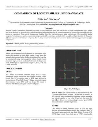
  • 1. IJRET: International Journal of Research in Engineering and Technology eISSN: 2319-1163 | pISSN: 2321-7308 __________________________________________________________________________________________ Volume: 02 Issue: 10 | Oct-2013, Available @ http://www.ijret.org 573 COMPARISON OF LOGIC FAMILIES USING NAND GATE Vibha Soni1 , Nitin Naiyar2 1, 2 Electronics & Telecommunication Engineering Department Rungta College of Engineering & Technology, Bhilai 490024, Chhattisgarh, India, vibhasoni178@rediffmail.com, naiyar16@gmail.com Abstract A digital circuit is constructed from small electronic circuits called logic gates that can be used to create combinational logic. A logic gate is an idealized or physical device which implements a Boolean function. It is an arrangement of electrically controlled switches, known as transistors. They are the fundamental building block for high performance data path circuits. The monolithic digital integrated circuit devices can be constructed using several different designs methods which use different logic families. In this paper different logic circuit families are compared. Power, delay and power-delay product are some of the performance parameters used for comparison. Keywords- CMOS, power, delay, power-delay product. ---------------------------------------------------------------------***------------------------------------------------------------------------- 1 INTRODUCTION A logic gate performs a logical operation on one or more logic inputs and produces a single logic output. Logic gates are primarily implemented using diodes or transistors but can also be constructed using electromagnetic relays, fluidic logic, pneumatic logic, or even mechanical elements. In the present work, NAND gate is implemented using RTL, DTL, TTL and CMOS structures. 2 LOGIC FAMILIES 2.1 RTL RTL stands for Resistor Transistor Logic. In RTL logic, transistor is used in conjunction with resistors to create a logic circuit. The NPN transistor used in RTL logic acts as an inverter circuit. When high (Logic „1‟) input is applied at gate, then transistor turns „ON‟ and low (logic 0‟) output is obtained. The RTL NAND gate is shown in figure 1. Fig. 1 RTL NAND gate An RTL NAND gate circuit consists of two transistors Q1 and Q2 connected as shown in figure 1. When both of input In1 or In2 is driven high, corresponding transistor goes to saturation and output is pulled to low value. When both the inputs In1 and In2 are driven low, corresponding transistor goes to OFF state and output is pulled to high value. 2.2 DTL DTL stands for Diode Transistor Logic. In DTL, the logic function is implemented using diodes and transistors. Each of the input is associated with one diode. Figure 2 shows DTL NAND logic circuit. Here diode acts as „AND‟ circuit and is
  • 2. IJRET: International Journal of Research in Engineering and Technology eISSN: 2319-1163 | pISSN: 2321-7308 __________________________________________________________________________________________ Volume: 02 Issue: 10 | Oct-2013, Available @ http://www.ijret.org 574 connected to a transistor inverter which acts as „NOT‟ circuit. According to inputs going high value, the corresponding diode conducts current, through the resistor. This turns „ON‟ the transistor. The transistor act as short circuit and is grounded. At the output, low value is obtained. If input In1 and In2 are Low, the diodes do not conduct and thus output is at High value. Fig. 2 DTL NAND gate 2.3 TTL TTL stands for Transistor-Transistor Logic. Figure 3 shows the TTL NAND gate. Fig. 3 TTL NAND gate When one of the inputs is high, the output is high; otherwise, the output is low. When both inputs In1 and In2 are high, the two transistors on the left are in reverse active state. A current flows through the resistor through the base and collector of these transistors, and then through the base of the transistor on the right, saturating it and bringing the output down near ground When both inputs In1 and In2 are low, the easiest path to ground through the resistor is through the base of the transistors on the left to the inputs. This brings their collector voltages low enough so that very little current can flow through the base of the transistor on the right. This keeps that transistor off, bringing the output to high. When only one of the inputs is low, that input provides the easiest path to ground, through its corresponding transistor. This keeps the transistor on the right switched off. 2.4 CMOS CMOS stands for complementary Metal Oxide Semiconductor. It uses complementary arrangements of N- channel and P-channel Field Effect Transistor. Since the initial devices used oxide-isolated metal gates, they are called CMOS. CMOS NAND gate is shown in figure 4. Fig. 4 CMOS NAND gate 3 RESULTS & DISSCUSSION The output waveforms are shown in figure 5. The x axis shows the voltage level in volts and y axis shows time in seconds. The input voltage level is given by V(in1) and V(in2). The corresponding NAND logic output can be observed from V(out). Thus it can be seen that if both of the two inputs are at high logic level, the corresponding output shows logic „1‟ and if both the inputs are low, then output is at logic „1‟. Simulations have been performed for RTL, DTL,
  • 3. IJRET: International Journal of Research in Engineering and Technology eISSN: 2319-1163 | pISSN: 2321-7308 __________________________________________________________________________________________ Volume: 02 Issue: 10 | Oct-2013, Available @ http://www.ijret.org 575 TTL and CMOS NAND logic. The output waveform shown in fig 5 is of CMOS NAND logic. Fig. 5 Output Waveforms Table 1 shows the comparison between RTL, DTL, TTL and CMOS logic families. The simulation had been carried out at power supply voltage value of 3 V. Power, delay, and power- delay products are few of the performance parameters considered here for comparison between various logic families. Table 1 Comparison of different logic families It can be observed from Table 1 that power dissipation in CMOS logic is least as compared to all the logic families. The power delay product which shows the figure of merit is least for CMOS technology and hence CMOS logic family outperforms all the logic families. Figure 6 shows the graphical representation of power consumption in different logic families. It can be seen that TTL logic families consume highest power and minimum power dissipation is in CMOS logic family. Fig. 6 Power dissipation in various logic families Figure 7 shows the graphical representation of delay in different logic families. It is observed that DTL logic family has the maximum delay compared to CMOS logic family. Fig. 7 Delay in various logic families Figure 8 shows the graphical representation of power- delay product in different logic families. It can be seen that though delay in CMOS is high than TTL, but power-delay product of CMOS is minimum compared to other logic families. Thus overall performance of CMOS logic family is better in comparison with other logic families. 0.00E+00 5.00E-04 1.00E-03 1.50E-03 2.00E-03 2.50E-03 3.00E-03 3.50E-03 4.00E-03 Power Power 0.00E+00 1.00E+01 2.00E+01 3.00E+01 4.00E+01 5.00E+01 6.00E+01 7.00E+01 8.00E+01 9.00E+01 Delay Delay
  • 4. IJRET: International Journal of Research in Engineering and Technology eISSN: 2319-1163 | pISSN: 2321-7308 __________________________________________________________________________________________ Volume: 02 Issue: 10 | Oct-2013, Available @ http://www.ijret.org 576 Fig. 8 Power dissipation product in various logic families CONCLUSIONS This paper provides comparison of different logic families in terms of power, delay and power-delay product. It has been observed that delay in CMOS logic family is high as compared to TTL logic family. The power consumption and power-delay product of CMOS logic families are minimum. Thus CMOS outperforms in performance parameters as compared to other logic families. REFERENCES [1] Soeleman, H., Roy, K. and Paul, B. C. "Robust Subthreshold Logic for Ultra-Low Power Operation," IEEE Transactions on Very Large Scale Integration (VLSI) Systems, vol. 9, no1, February 2001, pp. 90-99. [2] Kao J., Narenda S. and Chandrakasan A., "Subthreshold Leakage Modeling and Reduction Techniques," IEEE/ACM International Conference on Computer Aided Design (ICCAD), November 10-14, 2002, pp.141-148. [3] S. Yang, W. Wolf, N. Vijaykrishnan, T. Xie and W. Wang, "Accurate Stacking Effect Macro-Modeling of Leakage Power in Sub-100 nm Circuits," 18th International Conference on VLSI Design, 2005, pp. 165-170. [4] Y. Taur, “CMOS Scaling And Issues In Sub-0.25 Systems,” in Design of High-Performance Microprocessor Circuits, Eds. Piscataway, NJ: IEEE, 2001, pp. 27–45. [5] C. Molina, C. Aliagas, M. Garcia, A. Gonzalez, and J. Tubella, “Non Redundant Data Cache,” in Proc.Int. Symp.Low Power Electron Des., 2003, pp. 274–277. [6] R.Velagapudi, “Dual-tox Technique For Gate Leakage Reduction”. [7] S. Hanson, B. Zhai, K. Bernstein et al., “Ultralow-voltage Minimum-energy CMOS,” IBM Journal of Research and Development, vol. 50, no. 4-5, pp. 469–490, 2006. 0.00E+00 2.00E-02 4.00E-02 6.00E-02 8.00E-02 1.00E-01 1.20E-01 Power-Delay Product Power- Delay Product