MOS Transistor Fundamentals Explained
•Als PPTX, PDF herunterladen•
13 gefällt mir•18,868 views

The document discusses the MOS transistor and its operation. It begins by describing the components and structure of the MOS transistor, including the polysilicon gate, aluminum contacts, and silicon dioxide layer. It then discusses the energy band diagrams and how applying different gate voltages results in accumulation, depletion, or inversion at the surface. The document also covers the threshold voltage, its dependence on factors like doping and oxide thickness, and its impact on MOSFET operation. It concludes by deriving the MOSFET drain current equation using the gradual channel approximation approach.

Empfohlen
Weitere ähnliche Inhalte
Was ist angesagt?
Was ist angesagt? (20)
Ähnlich wie MOS Transistor Fundamentals Explained
Ähnlich wie MOS Transistor Fundamentals Explained (20)
Mehr von vidhya DS
Kürzlich hochgeladen
Kürzlich hochgeladen (20)
MOS Transistor Fundamentals Explained
- 2. Two-Terminal MOS Structure Tox is 2nm to 50nm
- 3. The equilibrium concentrations of mobile carriers in a semiconductor always obey the Mass Action Law n = the mobile carrier concentrations of electrons p= the mobile carrier concentrations of holes = the intrinsic carrier concentration of silicon, which is a function of the temp T. At room temperature, i.e., T= 300 K, =1.45 x 10^10 cm-3. Assuming that the substrate is uniformly doped with an acceptor (e.g.,Boron) concentration , the equilibrium electron and hole concentrations in the p-type substrate are approximated by in in AN (1) (2) 31615 10to10 cmNA
- 4. Energy Band Diagram of p-type Silicon Substrate
- 5. The band-gap between the conduction band and the valence band for silicon is approximately 1.1 eV. The location of the equilibrium Fermi level within the band-gap is determined by the doping type and the doping concentration in the silicon substrate. The Fermi potential , which is a function of temperature and doping, denotes the difference between the intrinsic Fermi level , and the Fermi level FE iE FE F (3)
- 6. For a p-type semiconductor, the Fermi potential can be approximated by For an n-type semiconductor (doped with a donor concentration ), the Fermi potential is given by DN The definitions given in (4) and (5) result in a positive Fermi potential for n-type material, and a negative Fermi potential for p-type material (4) (5)
- 7. The electron affinity of silicon, which is the potential difference between the conduction band level and the vacuum (free-space) level, is denoted by The energy required for an electron to move from the Fermi level into free space is called the work function , and is given bySq q (6)
- 8. Energy band diagrams of the MOS system Energy band diagrams of the components that make up the MOS system Mq oxideq siliconq= Work Function of Metal = Electron affinity of Silicon = Electron affinity of Oxide layer
- 9. Energy band diagram of the combined MOS system Flat Band Voltage:It is the voltage corresponding to the potential difference applied externally between the gate and the substrate, so that the bending of the energy bands near the surface can be compensated, i.e., the energy bands become "flat.” (7)
- 10. Assume that the substrate voltage is set at , and let the gate voltage be the controlling parameter. Depending on the polarity and the magnitude of , three different operating regions can be observed for the MOS system: Accumulation Depletion Inversion The MOS System under External Bias 0BV GV
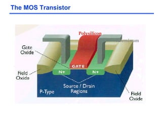
- 11. MOS gate Structure First electrode - Gate : Consists of low-resistivity material such as highly-doped polycrystalline silicon, aluminum or tungsten Second electrode - Substrate or Body: n- or p- type semiconductor Dielectric - Silicon dioxide: stable high-quality electrical insulator between gate and substrate.
- 12. Gate and Substrate Conditions for Different Biases Accumulation VG << VTN Depletion VG < VTN Inversion VG > VTN
- 13. Accumulation If a negative voltage is applied to the gate electrode, the holes in the p-type substrate are attracted to the semiconductor-oxide interface. The majority carrier concentration near the surface becomes larger than the equilibrium hole concentration in the substrate; hence, this condition is called carrier accumulation on the surface. Note that in this case, the oxide electric field is directed towards the gate electrode. The negative surface potential also causes the energy bands to bend upward near the surface. While the hole density near the surface increases as a result of the applied negative gate bias, the electron (minority carrier) concentration decreases as the negatively charged electrons are pushed deeper into the substrate. GV
- 14. The MOS System under External Bias (Accumulation) The cross-sectional view and the energy band diagram of the MOS structure operating in accumulation region
- 15. A small positive gate bias is applied to the gate electrode. Since the substrate bias is zero, the oxide electric field will be directed towards the substrate in this case. The positive surface potential causes the energy bands to bend downward near the surface. The majority carriers, i.e., the holes in the substrate, will be repelled back into the substrate as a result of the positive gate bias, and these holes will leave negatively charged fixed acceptor ions behind. Thus, a depletion region is created near the surface. Note that under this bias condition, the region near the semiconductor-oxide interface is nearly devoid of all mobile carriers. The MOS System under External Bias (Depletion) GV
- 16. The cross-sectional view and the energy band diagram of the MOS structure operating in depletion mode, under small gate bias The MOS System under External Bias (Depletion)
- 17. Depth of Depletion Region & Depletion Region Charge Density The mobile hole charge in a thin horizontal layer parallel to the surface is The change in surface potential required to displace this charge sheet by a distance away from the surface can be found by using the Poisson equationx dQ Integrating along the vertical dimension (perpendicular to the surface) yields The depth of the depletion region is: The depletion region charge density, which consists solely of fixed acceptor ions in this region, is given by (8) (9) (10) (11) (12)
- 18. The MOS System under External Bias (Inversion) If the positive gate bias is further increased i.e As a result of the increasing surface potential, the downward bending of the energy bands will increase as well. Eventually, the mid-gap energy level becomes smaller than the Fermi level on the surface, which means that the substrate semiconductor in this region becomes n-type. Within this thin layer, the electron density is larger than the majority hole density, since the positive gate potential attracts additional minority carriers (electrons) from the bulk substrate to the surface. The n-type region created near the surface by the positive gate bias is called the inversion layer, and this condition is called surface inversion. It will be seen that the thin inversion layer on the surface with a large mobile electron concentration can be utilized for conducting current between two terminals of the MOS transistor. )Large(0GV iE pFE
- 19. The surface is said to be inverted when the density of mobile electrons on the surface becomes equal to the density of holes in the bulk (p-type) substrate. This condition requires that the surface potential has the same magnitude, but the reverse polarity, as the bulk Fermi potential . Once the surface is inverted, any further increase in the gate voltage leads to an increase of mobile electron concentration on the surface, but not to an increase of the depletion depth. Thus, the depletion region depth achieved at the onset of surface inversion is also equal to the maximum depletion depth, , which remains constant for higher gate voltages. Using the inversion condition , the maximum depletion region depth at the onset of surface inversion can be found from (11) as follows The MOS System under External Bias (Inversion) The creation of a conducting surface inversion layer through externally applied gate bias is an essential phenomenon for current conduction in MOS transistors (13) F dmx FS
- 20. The cross-sectional view and the energy band diagram of the MOS structure in surface inversion, under larger gate bias voltage The MOS System under External Bias (Inversion)
- 21. Structure and Operation of MOS Transistor (MOSFET) The physical structure of an n-channel enhancement-type MOSFET
- 22. Circuit symbols Circuit symbols for n-channel and p-channel enhancement-type MOSFETs Circuit symbols for n-channel depletion-type MOSFETs
- 23. Formation of a depletion region Formation of a depletion region in an n-channel enhancement-type MOSFET
- 24. Band diagram of the MOS structure at Inversion Band diagram of the MOS structure underneath the gate, at surface inversion. Notice the band bending by at the surface.F2
- 25. Formation of an inversion layer Formation of an inversion layer (channel) in an n-channel enhancement-type MOSFET
- 26. For all practical purposes, there are four physical components of the threshold voltage: (i) the work function difference between the gate and the channel (ii) the gate voltage component to change the surface potential at inversion (iii) the gate voltage component to offset the depletion region charge (iv)the voltage component to offset the fixed charges in the gate oxide and in the silicon-oxide interface. The Threshold Voltage
- 27. The externally applied gate voltage is required to achieve surface inversion So the second component of the threshold voltage. FFS FS V 2 As 2 The work function difference between the gate and the channel reflects the built-in potential of the MOS system, which consists of the p-type substrate, the thin silicon dioxide layer, and the gate electrode. GC GCV 1 The first component of the threshold voltage The Threshold Voltage
- 28. The Threshold Voltage ox B C Q V 3 The third component that offsets the depletion region charge is Where is the gate oxide capacitance per unit area.oxC The depletion region charge density at surface inversion ( )FS The depletion region charge density can be expressed as a function of the source-to-substrate voltage SBV
- 29. The Threshold Voltage Due to the influence of a nonideal physical phenomenon, there always exists a fixed positive charge density at the interface between the gate oxide and the silicon substrate, due to impurities and/or lattice imperfections at the interface. Combining all of these voltage components oxQ ox ox C Q V 4 The (fourth) gate voltage component that is necessary to offset this positive charge at the interface is For zero substrate bias, the threshold voltage is expressed as follows 4321 VVVVVT 0TV With source-to-substrate bias voltage SBV
- 30. is the substrate-bias (or body-effect) coefficient The most general expression of the threshold voltage can be written as TV The generalized form of the threshold voltage can also be written as Where The Threshold Voltage (14)
- 31. The threshold voltage expression given can be used both for n-channel and p-channel MOS transistors. But some of the terms and coefficients in this equation have different polarities for the n-channel (nMOS) case and for the p-channel (pMOS) case. The reason for this polarity difference is that the substrate semiconductor is p-type in an n-channel MOSFET and n-type in a p-channel MOSFET. The substrate Fermi potential is negative in nMOS, positive in pMOS. The depletion region charge densities and are negative in nMOS, positive in pMOS. The substrate bias coefficient is positive in nMOS, negative in pMOS. The substrate bias voltage is positive in nMOS, negative in pMOS. Typically, the threshold voltage of an enhancement-type n-channel MOSFET is a positive quantity, whereas the threshold voltage of a p-channel MOSFET is negative. The Threshold Voltage F 0BQ BQ SBV
- 33. The exact value of the threshold voltage of an actual MOS transistor cannot be determined using (14) in most practical cases, due primarily to uncertainties and variations of the doping concentrations, the oxide thickness, and the fixed oxide-interface charge. The nominal value and the statistical range of the threshold voltage for any MOS process are ultimately determined by direct measurements, which will be described later. In most MOS fabrication processes, the threshold voltage can be adjusted by selective dopant ion implantation into the channel region of the MOSFET. For n-channel MOSFETs, the threshold voltage is increased (made more positive) by adding extra p-type impurities (acceptor ions). Alternatively, the threshold voltage of the n-channel MOSFET can be decreased (made more negative) by implanting n-type impurities (dopant ions) into the channel region The Threshold Voltage
- 34. Substrate –bias Effect on Threshold Voltage It is seen that the threshold voltage variation is about 1.3 V over this range, which could present serious design problems if neglected. So the substrate-bias effect is unavoidable in most digital circuits and that the circuit designer usually must take appropriate measures to account for and/or to compensate for the threshold voltage variations.
- 35. Substrate –bias Effect on Threshold Voltage
- 36. MOSFET Operation: A Qualitative View Cross-sectional view of an n-channel (nMOS) transistor, (a) operating in the linear region, (b) operating at the edge of saturation, and (c) operating beyond saturation
- 37. Cross-sectional view of an n-channel (nMOS) transistor operating in the linear region
- 38. Cross-sectional view of an n-channel (nMOS) transistor operating at the edge of saturation
- 39. Cross-sectional view of an n-channel (nMOS) transistor operating beyond saturation
- 40. The analytical derivation of the MOSFET current-voltage relationships for various bias conditions requires that several approximations be made to simplify the problem. Without these simplifying assumptions, analysis of the actual three- dimensional MOS system would become a very complex task and would prevent the derivation of closed form current-voltage equations. MOSFET Current-Voltage Characteristics
- 41. MOSFET Current-Voltage Characteristics Cross-sectional view of an n-channel transistor, operating in linear region.
- 42. Gradual Channel Approximation(GCA) Consider the cross-sectional view of the n-channel MOSFET operating in the linear mode, as shown in the figure. Here, the source and the substrate terminals are connected to ground, i.e., Vs = VB = 0. The gate-to-source voltage (VGS) and the drain-to-source voltage (VDS) are the external parameters controlling the drain (channel) current ID. The gate-to-source voltage is set to be larger than the threshold voltage VT0 to create a conducting inversion layer between the source and the drain. The gradual channel approximation (GCA) for establishing the MOSFET current-voltage relationships, effectively reduces the analysis to a one- dimensional current-flow problem. As in every approximate approach, however, the GCA also has its limitations, especially for small-geometry MOSFETs.
- 43. The boundary conditions for the channel voltage Vc are: Assumption: The entire channel region between the source and the drain is inverted, i.e., The channel voltage with respect to the source is denoted by Vc(y). Assumption: The threshold voltage VT0 is constant along the entire channel region, between y = 0 and y = L. (In reality, the threshold voltage changes along the channel since the channel voltage is not constant) Assumption: The electric field component Ey along the y-coordinate is dominant compared to the electric field component Ex along the x-coordinate. (This assumption will allow us to reduce the current-flow problem in the channel to the y dimension only) Gradual Channel Approximation(GCA)
- 44. The thickness of the inversion layer tapers off as we move from the source to the drain, since the gate-to-channel voltage causing surface inversion is smaller at the drain end. Simplified geometry of the surface inversion layer (channel region) MOSFET Drain Current Equation(GCA) Let QI(y) be the total mobile electron charge in the surface inversion layer. This charge can be expressed as a function of the gate-to-source voltage VGS and of the channel voltage Vc(y) as follows (15)
- 45. The incremental resistance dR of the differential channel segment can be expressed as (assuming constant surface mobility of all mobile electrons in the inversion layer) Applying Ohm's law for this segment yields the voltage drop along the incremental segment dy, in the y direction. MOSFET Drain Current Equation(GCA) n The minus sign is due to the negative polarity of the inversion layer charge QI (16) (17) nq xyqnxyQ n ccI 11 ]yatdepthchannelarea;y-unit W[per)()(
- 46. MOSFET Drain Current Equation(GCA) Integrating along the Channel (18) (20) (19)
- 47. Equation (20) represents the drain current ID as a simple second-order function of the two external voltages, VGS and VDS. This current equation can also be rewritten as or where the parameters k and k' are defined as Current-voltage relationship is affected by to the process dependent constants k' , VT0, and is also affected by the device dimensions, W and L. MOSFET Drain Current Equation(GCA) (21) (22) process transconductance parameter gain factor
- 48. Region of Validity of the Equation The second-order current-voltage equation given above produces a set of inverted parabolas for each constant VGS value. The drain current-drain voltage curves shown above reach their peak value for VDS = VGS – VT0 Beyond this maximum, each curve exhibits a negative differential conductance, which is not observed in actual MOSFET current-voltage measurements (section shown by the dashed lines)
- 49. We must remember now that the drain current equation (20) has been derived under the following voltage assumptions, which guarantee that the entire channel region between the source and the drain is inverted. This condition corresponds to the linear operating mode for the MOSFET Hence, the current equation (20) is valid only for the linear mode operation. Validity of the Equation (Linear Region)
- 50. VDS~ ID Curve
- 51. It is to be noted that the VDS measured relative to the source increases from 0 to VDS as we travel along the channel from source to drain. This is because the voltage between the gate and points along the channel decreases from VGS at the source end to VGS-VDS. When VDS is increased to the value that reduces the voltage between the gate and channel at the drain end to VT that is , VGS-VDS=VT or VDS= VGS-VT or VDS(sat) ≥ VGS-VT Concept of Asymmetric Channel
- 52. MOSFET Current –Voltage Characteristics (Saturation Region) When VDS is increased to the value that reduces the voltage between the gate and channel at the drain end to Vt that is , VGS-VDS=VT or VDS= VGS-VT At this point the channel depth at the drain end decreases to almost zero, and the channel is said to be pinched off. Increasing VDS beyond this value has no effect on the channel shape. The MOSFET is said to have entered the saturation region, the drain current is essentially independent of VDS for constant VGS. VDSsat= VGS-VT Obviously, for every value of VGS≥VT, there is a corresponding value of VDSsat
- 53. Current Equation for Saturation Region Beyond the linear region boundary, i.e., for VDS values larger than VGS - VT0, the MOS transistor is assumed to be in saturation. When Definition Condition for Saturation (23) This expression indicates that the saturation drain current has no dependence on VDS 0 0 0)()( TGSDSAT DSATTGSoxI VVV VVVCLyQ
- 55. Consequently, the effective channel length (the length of the inversion layer where GCA is still valid) is reduced to Where is the length of the channel segment with QI = 0L Channel Length Modulation The inversion layer charge at the source end of the channel is The inversion layer charge at the drain end of the channel is Note that at the edge of saturation, i.e., when the drain-to-source voltage reaches VDSAT,
- 56. Since QI(y) = 0 for L’ < y < L, the channel voltage at the pinch-off point remains equal to VDSAT The gradual channel approximation is valid in this region; thus, the channel current can be written Thus, (24) accounts for the actual shortening of the channel, also called channel length modulation. Channel Length Modulation (24) (25) The first term of this saturation current expression accounts for the channel modulation effect, while the rest of this expression is identical to (23).
- 57. is an empirical model parameter, and is called the channel length modulation coefficient. Assuming that Since Channel Length Modulation (26) Empirically Equation (25) becomes