Ade manual final
•Als DOC, PDF herunterladen•
2 gefällt mir•14,131 views

UPTU/MTU/GBTU Lab manual for ADE lab 2nd year

Empfohlen
Weitere ähnliche Inhalte
Was ist angesagt?
Was ist angesagt? (20)
Andere mochten auch
Andere mochten auch (9)
Ähnlich wie Ade manual final
Ähnlich wie Ade manual final (20)
Kürzlich hochgeladen
Kürzlich hochgeladen (20)
Ade manual final
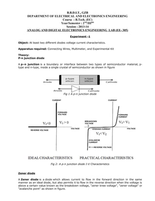
- 1. B.B.D.I.T., GZB DEPARTMENT OF ELECTRICAL AND ELECTRONICS ENGINEERING Course : B.Tech. (EC) Year/Semester : 2ND/IIIRD Session : 2013-14 ANALOG AND DIGITAL ELECTRONICS ENGINEERING LAB (EE- 305) Experiment -1 Object: At least two different diodes voltage current characteristics. Apparatus required: Connecting Wires, Multimeter, and Experimental Kit Theory: P-n junction diode A p–n junction is a boundary or interface between two types of semiconductor material, ptype and n-type, inside a single crystal of semiconductor as shown in figure Fig 1 A p-n junction diode Fig 2: A p-n junction diode I-V Characteristics Zener diode A Zener diode is a diode which allows current to flow in the forward direction in the same manner as an ideal diode, but also permits it to flow in the reverse direction when the voltage is above a certain value known as the breakdown voltage, "zener knee voltage", "zener voltage" or "avalanche point" as shown in figure.
- 2. Fig 3 Symbol of Zener Diode Fig 4: I-V Characteristics Zener Diode with Breakdowns Observational Table: 1) P-n junction diode S.No. 2) Voltage Current Voltage Current Zener diode S.No. Result: The characteristics of the two diodes have been verified and shown in the graph paper Precautions: 1 .Donot touch live wires. 2. Power supply switched OFF after completing experiment.
- 3. B.B.D.I.T., GZB DEPARTMENT OF ELECTRICAL AND ELECTRONICS ENGINEERING Course : B.Tech. (EC) Year/Semester : 2ND/IIIRD Session : 2013-14 ANALOG AND DIGITAL ELECTRONICS ENGINEERING LAB (EE- 305) Experiment -2 Object: To make discrete component AND and OR gate using Transistor. Apparatus required: Connecting Wires, Transistors, Bread board and Resistances etc. Theory: AND gate – The AND gate is a basic digital logic gate that implements logical conjunction - it behaves according to the truth table to the right. A HIGH output (1) results only if both the inputs to the AND gate are HIGH (1). If neither or only one input to the AND gate is HIGH, a LOW output results. In another sense, the function of AND effectively finds the minimum between two binary digits, just as the OR function finds the maximum. Therefore, the output is always 0 except when all the inputs are 1s. Connect two transistors in a way that the output is high only when both inputs are high. Fig 1 AND Gate Symbol, Truth table, Transistor equivalent OR gate – The OR gate is a digital logic gate that implements logical disjunction - it behaves according to the truth table to the right. A HIGH output (1) results if one or both the inputs to the gate are HIGH (1). If neither input is HIGH, a LOW output (0) results. In another sense, the function of OR effectively finds the maximum between two binary digits, just as the complementary AND function finds the minimum This is simpler, connect them in a way that when either input is high the output will be high.
- 4. Fig 2: OR Gate Symbol, Truth Table and Transistor Equvalent Result: Precautions: 1. Connections should be tight. 2. Take care when applying proper supply.
- 5. B.B.D.I.T., GZB DEPARTMENT OF ELECTRICAL AND ELECTRONICS ENGINEERING Course : B.Tech. (EC) Year/Semester : 2ND/IIIRD Session : 2013-14 ANALOG AND DIGITAL ELECTRONICS ENGINEERING LAB (EE- 305) Experiment No.-3 Object: To study R-C-Coupled amplifier, frequency characteristics to determine lower and upper cut off frequencies & band width. Equipment Used: 1. CRO 2. FET Amplifier Kit 3. A F Generator 4. Multimeter 5. Connecting wires Theory: An FET can also be used as an amplifier like the ordinary transistor. FET has the extra advantage of high input impedance It finds extensive application as single stage amplifier in measuring instruments due to its high input Impedance. So far as the input impedance is concerned the FET behaves like a vacuum tube pentode. Fig. a, shows the circuit diagram of a common source amplifier with self-biasing. The capacitor C 1 &C2 are coupling capacitors which prevents any external DC voltage from disturbing the bias conditions of FET amplifier. The capacitor Cs acts as the AC bypass capacitor across Rs and serves the same purpose as C E in a common emitter amplifier. If Cs is disconnected then negative feedback takes place and the gain of the circuit reduces. Circuit Diagram: Fig 1: FET based RC Coupled Amplifier
- 6. Fig 2: Frequency response of FET Amp. Fig 3: Without Feedback Frequency response Observation Table: S.No. Frequency V1 I/P V0 S0 OFF (Without-feedback) Av =Vo/Vi (Without-Feed back) Procedure of Experiment: 1. Draw the circuit diagram of this single stage R-C coupled Amplifier your note book and implement this circuit on the kit
- 7. 2. Make the following: T8 to T1, T5 to T3, and T 3 to T4 Keep switch S0 in ON position and remove the shorting link between T9&T2VGG is not to be connected now. Connect V DD between T5&T2 set its value to about 15 volts. This makes the circuit of a common source amplifier with T 7-T12As Input Port T11-T6 as output port. 3.Measure the DC voltages at T3 &T2 with respect to T6 & record them as VD &Vs respectively. These voltages give you the DC bias point. 4. Connect a AF Oscillator at Input Port with its frequency adjusted to 1KHz. 5. Connect a C.R.O. at the output port & adjust the input signal amplitude so as to get undistorted output on C.R.O. 6. Measure the voltage gain by Measuring output &input amplitudes on the C.R.O. at different signal frequency. This will give you the frequency responses of the amplifier without feedback. 7. Switch OFF So. This disconnects the by-pass capacitor Cs & negative feedback is introduced. Repeat steps-4 to 6 for this conduction. Calculation of Bandwidth BW=f2-f1 Result: The frequency response shown in the semilog graph paper. Precautions: 1. Switch off power supply before making any interconnections on the board. 2. Use proper leads only for interconnections. 3. If the dc supply is not coming then it may be due to short circuiting in the connections. Remove the connections in such a case and check the dc supply.
- 8. B.B.D.I.T., GZB DEPARTMENT OF ELECTRICAL AND ELECTRONICS ENGINEERING Course : B.Tech. (EC) Year/Semester : 2ND/IIIRD Session : 2013-14 ANALOG AND DIGITAL ELECTRONICS ENGINEERING LAB (EE- 305) Experiment No.-4 Object: To study the effect of negative feedback on the characteristics of R-C-Coupled amplifier. Equipment Used: 1. CRO 2. FET Amplifier Kit 3. A F Generator 4. Multimeter 5. Connecting wires Theory: An FET can also be used as an amplifier like the ordinary transistor. FET has the extra advantage of high input impedance It finds extensive application as single stage amplifier in measuring instruments due to its high input Impedance. So far as the input impedance is concerned the FET behaves like a vacuum tube pentode. Fig. a, shows the circuit diagram of a common source amplifier with self-biasing. The capacitor C 1 &C2 are coupling capacitors which prevents any external DC voltage from disturbing the bias conditions of FET amplifier. The capacitor Cs acts as the AC bypass capacitor across Rs and serves the same purpose as C E in a common emitter amplifier. If Cs is disconnected then negative feedback takes place and the gain of the circuit reduces. Circuit Diagram: Fig RC Coupled Amplifier
- 9. Fig: Frequency response of FET Amp. Fig: Response with feedback Observation Table: S.No. Frequency V1 I/P V0 S0 ON (With-Feedback) Av =Vo/Vi (With Feedback) Procedure of Experiment: 1. Draw the circuit diagram of this single stage R-C coupled Amplifier your note book and implement this circuit on the kit
- 10. 2. Make the following: T8 to T1, T5 to T3, and T 3 to T4 Keep switch S0 in ON position and remove the shorting link between T9&T2VGG is not to be connected now. Connect V DD between T5&T2 set its value to about 15 volts. This makes the circuit of a common source amplifier with T 7-T12As Input Port T11-T6 as output port. 3.Measure the DC voltages at T3 &T2 with respect to T6 & record them as VD &Vs respectively. These voltages give you the DC bias point. 4. Connect a AF Oscillator at Input Port with its frequency adjusted to 1KHz. 5. Connect a C.R.O. at the output port & adjust the input signal amplitude so as to get undistorted output on C.R.O. 6. Measure the voltage gain by Measuring output &input amplitudes on the C.R.O. at different signal frequency. This will give you the frequency responses of the amplifier without feedback. 7. Switch OFF So. This disconnects the by-pass capacitor Cs & negative feedback is introduced. Repeat steps-4 to 6 for this conduction. Calculation of Bandwidth BW=f2-f1 Result: The frequency response shown in the semilog graph paper. Precautions: 1. Switch off power supply before making any interconnections on the board. 2. Use proper leads only for interconnections. 3. If the dc supply is not coming then it may be due to short circuiting in the connections. Remove the connections in such a case and check the dc supply.
- 11. B.B.D.I.T., GZB DEPARTMENT OF ELECTRICAL AND ELECTRONICS ENGINEERING Course : B.Tech. (EC) Year/Semester : 2ND/IIIRD Session : 2013-14 ANALOG AND DIGITAL ELECTRONICS ENGINEERING LAB (EE- 305) Experiment No:5 Object: Design a RC Phase-Shift sinusoidal Oscillator and to study its wave shape. Apparatus: C.R.O, OP-Amp 741,Resistance (33kΩ 3.3k Ω) Port 2M Ω, Capacitor (.013μF, 0.1 μF), Bread Board. Theory: In fig a Phase Shift Oscillator is shown as frequency selective network. The Phase Shift Oscillator is the standard oscillator circuit for all low to moderate frequencies, in the range of 5Hz to about 1MHz. Phase Shift Oscillator is proved positive feedback. Phase Shift Oscillator loop gain ßA to be greater than unity the gain of the amplifier stage must be greaterthan1/ß or 29. A>29 When considering the operation of the feedback network, one mighty naively selects the values of R&C to provide 60◦ phase shift per section for the three sections, resulting in a 180 ◦ phase shift. The frequency is dependent on R&C component Circuit: Fig 1: Basic Circuitry RC Phase Shift Oscillator
- 12. Fig 2: Kit level diagram of RC phase shift oscillator Calculation: Fp= 1/2πRC√6f FT=1/T Observation Table: R C FP FT Result: % error = (FT-FP)/FT *100 Precaution: 1. Switch off power supply before making any interconnections on the board. 2. Use proper leads only for interconnections. 3. If the dc supply is not coming then it may be due to short circuiting in the connections. Remove the connections in such a case and check the dc supply.
- 13. B.B.D.I.T., GZB DEPARTMENT OF ELECTRICAL AND ELECTRONICS ENGINEERING Course : B.Tech. (EC) Year/Semester : 2ND/IIIRD Session : 2013-14 ANALOG AND DIGITAL ELECTRONICS ENGINEERING LAB (EE- 305) EXPERIMENT 6 Object: - To study the characteristic of commercial D, T. & J-K Flip-Flops and to verify the truth table. Apparatus Required: i) ii) iii) Experimental Kit Connecting wires IC 7474(D), 74126(T), IC 7476(JK) Procedure: 1. Connections are made as per circuit diagram. 2. Verify the truth table for various combinations of inputs. Circuit Diagram& Truth table: i) D Flip-Flop Fig 1 Edge Triggered NAND BASED D Flip-Flop Fig:2 Logic Symbol D Flip-Flop
- 14. CLK Positive Edge Positive Edge 0 D 0 0 1 1 * * Qn 0 1 0 1 0 1 Qn+1 0 0 1 1 0 1 State Reset Set No Change Truth Table Edge Triggered NAND based D Flip-Flop ii) T Flip-flop Fig 3 Edge Triggered NAND BASED T Flip-Flop Fig 4: Logic Symbol T Flip-Flop CLK Positive Edge Positive Edge 0 T 0 0 1 1 * * Qn 0 1 0 1 0 1 Qn+1 0 1 1 0 0 1 Edge Triggered NAND BASED T Flip-Flop Truth Table State No Change Set No Change
- 15. Fig 5: Positive Edge triggered NAND based JK Flip-Flop Fig 6: Logic Diagram Positive Edge triggered NAND based JK Flip-Flop CLK Positive Edge Positive Edge Positive Edge Positive Edge 0 0 J 0 0 0 0 1 1 1 1 * * K 0 0 1 1 0 0 1 1 * * Qn 0 1 0 1 0 1 0 1 0 1 Qn+1 0 1 0 0 1 1 1 0 0 1 State No Change Reset Set Toggle No Change Fig 7: Truth Table of Positive Edge triggered NAND based JK Flip-Flop Result: The D, T, JK Flip Flop are successfully verified. Precautions: 1. 2. 3. 4. Connect the wires properly. Experiments should be performed under proper guidance and surveillance. Check the IC numbers correctly Switch ON the power supply only after the proper correction is made.
- 16. B.B.D.I.T., GZB DEPARTMENT OF ELECTRICAL AND ELECTRONICS ENGINEERING Course : B.Tech. (EC) Year/Semester : 2ND/IIIRD Session : 2013-14 ANALOG AND DIGITAL ELECTRONICS ENGINEERING LAB (EE- 305) Experiment 7 Object: To make mod10 ripple counters using commercial chip & record its performance & wave shape. APPARATUS REQUIRED: 1. JK FLIP FLOP IC 7476 (2) 2. NAND GATE IC 7400 1 3. IC TRAINER KIT 4. PATCH CORDS THEORY: A counter is a register capable of counting number of clock pulse arriving at its clock input. Counter represents the number of clock pulses arrived. A specified sequence of states appears as counter output. This is the main difference between a register and a counter. There are two types of counter, synchronous and asynchronous. In synchronous common clock is given to all flip flop and in asynchronous first flip flop is clocked by external pulse and then each successive flip flop is clocked by Q or Q output of previous stage. A soon the clock of second stage is triggered by output of first stage. Because of inherent propagation delay time all flip flops are not activated at same time which results in asynchronous operation.
- 17. Fig 2:Logic diagram for 4Bit Ripple Counter Fig 3: Mod 10 Ripple Counter Truth Table: MOD 10 Counter
- 18. Fig 5: Wave Shapes Mod 10 Ripple Counter Result: The MOD-10 Counter has been studied and the waveforms are recorded successfully. Precautions: 5. 6. 7. 8. Connect the wires properly. Experiments should be performed under proper guidance and surveillance. Check the IC numbers correctly Switch ON the power supply only after the proper correction is made.
- 19. B.B.D.I.T., GZB DEPARTMENT OF ELECTRICAL AND ELECTRONICS ENGINEERING Course : B.Tech. (EC) Year/Semester : 2ND/IIIRD Session : 2013-14 ANALOG AND DIGITAL ELECTRONICS ENGINEERING LAB (EE- 305) Experiment -8 Object: To make a synchronous counter of mod 4 and study its wave shape. Convert it into a ring counter. Apparatus Required: IC7408, IC7476, IC7400, IC7432, Bread board, Connecting wires. Theory: Synchronous Counter, the external clock signal is connected to the clock input of EVERY individual flip-flop within the counter so that all of the flip-flops are clocked together simultaneously (in parallel) at the same time giving a fixed time relationship. In other words, changes in the output occur in "synchronization" with the clock signal. This results in all the individual output bits changing state at exactly the same time in response to the common clock signal with no ripple effect and therefore, no propagation delay. Synchronous Counter as shown in figure. Fig 1: Binary 4-bit Synchronous Counter
- 20. The output of shift registers back to its input so that the output from the last flipflop, QD becomes the input of the first flip-flop, DA. We would then have a closed loop circuit that "recirculates" the DATA around a continuous loop for every state of its sequence, and this is the principal operation of a Ring Counter. Then by looping the output back to the input, we can convert a standard shift register into a ring counter. Consider the circuit below. Fig 2: 4-bit Ring Counter Fig 3: 4-bit Synchronous Counter Waveform Timing Diagram. Result: MOD-4 Synchronous Counter has been studied along with the wave shapes. Precaution: 1. Donot touches live wires. 2. Power supply switched OFF after completing experiment
- 21. B.B.D.I.T., GZB DEPARTMENT OF ELECTRICAL AND ELECTRONICS ENGINEERING Course : B.Tech. (EC) Year/Semester : 2ND/IIIRD Session : 2013-14 ANALOG AND DIGITAL ELECTRONICS ENGINEERING LAB (EE- 305) Experiment No.-10 OBJECT: Obtain a Schmitt trigger and study its characteristics for different input levels. EQUIPMENTS REQUIRED: Experimental board on transfer characteristics of Schmitt trigger Model – D518. THEORY: Fig. Shows a regenerative comparator this is known as Schmitt trigger. The input voltage Vi triggers the o/p Vo every time it exceed certain voltage level. The voltage levels are called as upper threshold voltage (V ht) &lower threshold voltage (V lt). The hysteresis width is the difference between these two threshold voltages V ht – Vlt . these threshold voltage are calculated as follows. Suppose Vo= Vsat, The voltages are at (+) input terminal can be obtained using superposition theorem, Vht=Vref{R1/(R1+R2)}+VsatR2{R2/(R1+R2)} If Vo= -Vsat . The voltage at the (+) input terminal is Vlt= Vref{R1/(R1+R2)}-VsatR2{R2/(R1+R2)} As long as Vi is less than Vut , the o/p Vo remains constant . PROCEDURE: 1) We vary the input voltage from minimum to maximum and take reading of output voltage. 2) We note down the input voltage at which output goes low. 3) Now we vary the input voltage from maximum to minimum and take the reading of output voltage. 4) We note down the input voltage at which output goes High..
- 22. OBSERVATIONS: Vi Vo CALCULATIONS: RESULT: We have obtained the transfer characteristics of Schmitt trigger successfully. PRECAUTIONS: 1) Vary the input voltage very slowly. 2) Readings should be taken carefully.
- 23. Experiment No. 3 Object: To Study the RC Coupled Amplifier, frequency charecteristics to determine lower and upper cut-off frequencies and bandwidth. Apparatus: CRO, RC Coupled Amplifier Kit, AF Oscillator, multimeter, Connecting wires. Theory: Most of the signal low power amplifier at low or high frequency make use of RC Coupling network does not couple the dc output of one state to other but it does modify the frequency response of the amplifier Fig-a as shows a single stage RC coupled transistor amplifier CE is called the emitter bypass capacitor the biasing resistor R1,R2 emitter resistor RE and collector resistor Rc. Frequency Response: The gain of an the amplifier circuit is not same for all frequencies. A plot of voltage gain as a function of frequency is called the frequency response of the amplifier. A typical frequency response curve for signal RC coupled amplifier is shown in Fig-b .As can be seen the whole curve can be divided into three parts 1- Low frequency region 2- Mid frequency region 3- High frequency region Circuit:
- 24. Fig-a (with-out feedback) (with feedback) Fig-b Observation Table: With-feedback (a) S.No. Frequency V1 I/P V0 (S1 L) (With-feedback) Av =Vo/Vi (With-Feedback)
- 25. Without-feedback (b) S.No. Frequency V1 I/P Result: 1-Frequency response V0 (S1 R) (Without-Feed back) Av =Vo/Vi (Without Feed back) Experiment No.-12 OBJECT: Make multivibrators using 555 chip. Study of IC 555 as a mono stable (one shot) Multivibrator. EQUIPMENTS REQUIRED: Analog board of AB28, DC power supplies + 5V, from external source or ST2612 Analog Lab, 2 mm patch cords, Ohm meter, Function generator [for pulse signal (Scientech Function Generator ST4062,ST4063 etc.)] THEORY: The functional diagram of 555 timer has two comparators UC (upper comparator) and LC (lower comparator), whose threshold voltages are 2Vcc/3 and Vcc/3 respectively, one SR flip flop (FF), a npn transistor , a pnp transistor, a power amplifier (act as a inverter). When input is applied to 2 pin of IC and as its –ive excursion crosses Vcc/3 LC will set the FF which makes output 1(high). FF output will off the transistor which realize the short circuit across capacitor (C) and it starts charging towards power supply. When the voltage of capacitor or at pin 6 reaches 2Vcc/3 in +ive excursion UC resets the FF and output becomes 0 (low). Since for another pulse at output a new trigger input is applied to pin 2 . therefore it is called monostable multivibrator.
- 26. PROCEDURE: Connect power supply + 5V from ST2612 or any external source. 1. Connect point a to point b using a 2mm patch cord. 2. Connect point c to point d/e using a 2mm patch cord. 3. Keep the pot (R2 1M) to fully anticlockwise direction. 4. Apply a pulse signal of 5Vpp and 1 KHz (keep duty cycle of pulse 50%) at pin 2 of IC 555 i.e. to the point e/g on AB28 board. Observe the same on oscilloscope CHI. 5. Connect pin 3 of IC55 i.e. output socket to the oscilloscope CHII. 6. Vary the pot and observe the variation of output pulse duty cycle with the change in resistance R (where, R=R1+R2). 7. For any value of R measure the ON time of output pulse. 8. Calculate the same by following equation for theoretically calculating the output pulse ‘On’ time. TP = 1.1 * R1C1 Note : For calculating the value of R, disconnect the +5V supply and connection between point a and b. Connect ohmmeter between point a and TP1. The ohmmeter will read the value of R. 9. Verify theoretical and practical values of TP. Note : The two values of TP (theoretical and practical values) will match only for time for which input pulse is High i.e. only for ‘On’ 'time of input pulse. To verify this vary the duty cycle of input signal and check the output pulse duty cycle by varying R (R=R1+R2). 10. Repeat above procedure for different values of R. CALCULATION: Find out time period of output pulse using the formula T = 1.1 RC sec RESULT: The time period is _______________ sec PRECAUTIONS: 1. Do not make connections on the board with power switched on.
- 27. 2. Do not make loose connection. OBJECT: Study of IC 555 as a astable (free running) Multivibrator. EQUIPMENTS REQUIRED: Analog board of AB28, DC power supplies + 5V, from external source or ST2612 Analog Lab, 2 mm patch cords. THEORY: The functional diagram of 555 timer has two comparators UC (upper comparator) and LC (lower comparator), whose threshold voltages are 2Vcc/3 and Vcc/3 respectively, one SR flip flop (FF), a npn transistor , a pnp transistor, a power amplifier (act as a inverter). When input is applied to 2 pin of IC and as its –ive excursion crosses Vcc/3 LC will set the FF which makes output 1(high). FF output will off the transistor which realize the short circuit across capacitor (C) and it starts charging towards power supply. When the voltage of capacitor or at pin 6 reaches 2Vcc/3 in +ive excursion UC resets the FF and output becomes 0 (low) which again make a short circuit across the capacitor and capacitor starts discharging towards ground. On discharging as its voltage reaches Vcc/3 LC sets FF which again make output 1(high) and the cycle repeats itself. Since it gives pulses at output hence it is called astable multivibrator. PROCEDURE: Connect power supply +5V from ST2612 or any external source. 1. Connect point a to point b using a 2mm patch cord. 2. Connect point d to point f/g using a 2mm patch cord. 3. Keep the pot (R2 1M) to fully anticlockwise direction.
- 28. 4. Connect pin 3 of IC55 i.e. output socket to the oscilloscope. 5. Vary the pot and observe the variation of output signal’s frequency with the change in resistance R (where, R=R1+R2). 6. To verify the above calculate the frequency of output signal using following equation • Note : For calculating the value of R, disconnect the +5V supply and connection between point a and b. Connect ohmmeter between point a and TP1. The ohmmeter will read the value of R. 7. Trace the waveforms of the voltage across capacitor C1 and ground. 8. Repeat above procedure for different values of R. CALCULATION: Find out time period of output pulse using the formula T = 0.69 (R + R3)C1 sec and frequency (f) = 1/ T. RESULT: The time period is _______________ sec Frequency is __________________ Hz PRECAUTIONS: 1) Do not make connections on the board with power switched on. 2) Do not make loose connection.