
Empfohlen
Empfohlen
Weitere ähnliche Inhalte
Was ist angesagt?
Was ist angesagt? (18)
Ähnlich wie NanowireSensor
Ähnlich wie NanowireSensor (20)
Mehr von dalgetty
Kürzlich hochgeladen
Kürzlich hochgeladen (20)
NanowireSensor
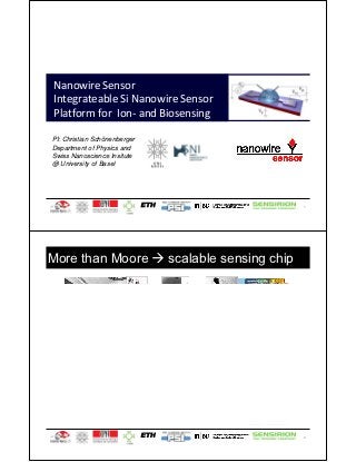
- 1. Nanowire Sensor Integrateable Si Nanowire Sensor Platform for Ion‐ and Biosensing PI: Christian Schönenberger Department of Physics and Swiss Nanoscience Insitute @ University of Basel 1 More than Moore scalable sensing chip 2
- 2. Bio- / chemical Sensor a device that can detect molecules in a with some specificity how can this information be read ? mechanically a) mass change (QCM) b) strain (cantilever) optically a) labelled (DNA chip) b) refractive index c) Plasmonics electrically a) impedance spectroscopy b) CV spectroscopy c) potentiometric (e.g. zeta potential) 3 Potentiometric Sensing IS-FET P. Bergveld / Sensors and Actuators B 88 1–20 (2003) 4
- 3. Ion Sensitive FET (IS-FET) channel conductance (i.e. threshold) depends on gate charge e.g. heparime binding on protamie p-channel, threshold regime - - - (source-drain current) - SHIFT source drain - - - (gate potential) 5 Electronic Biochip Concept Bergveld and others not C. Lieber et al. one ... .... .... but m any 6
- 4. Project fabrication technology (PSI, Basel, EPFL) surface functionalization (FHNW, ETHZ Basel‐Pharma) on-chip and system microfluidics simulation integration (ETHZ, Basel) electrical characterization (D‐BSSE, EPFL) and biochemical validation (all) 7 NW fabrication p-type (100) SOI > 30 nm SiO2 ~ 10 – 25 nm Si 40 – 85 nm buried SiO2 (BOX) 350 nm Si handle wafer 300 nm Cr mask HSQ resist contact masks ion implantation 70 nm SiO2 plasma etching in CHF3 Al contact annealing Si wet etching in TMAH 8
- 5. NW fabrication accumulation inversion (non‐implanted, Al‐contacts) 9 NW fabrication Novel fabricated GAA (gate all around) SiNWs SS = 62 mV/dec Ion/Ioff = 105-106 S.Rigante, M.Najmzadeh and A. M. Ionescu, EPFL 10
- 7. Results: Nernst limit vs liquid gate vs back gate µ ¶ kT ±Vlg−shif t = ±pHB 2.3 ·α q µ ¶ Cdl,ox corrected ±Vbg−shif t = ±Vlg−shif t Cbg O. Knopfmacher et al. Nano Lett. 10, 2268 (2010) 15 Results: Noise Measurements C. Beenakker and C. Schönenberger, Physics Today, Vol. 56, issue 5, page 37-42 (2003) FFT Tarasov et al. , APL, 98, 012114, (2011) 16
- 8. Results: Noise Measurements threshold noise: 400 ppm of pH Tarasov et al. , APL, 98, 012114, (2011) 17 Functionalized surface R1=NH2, Cl, CH3 bare alumina: 45‐55 mV/pH a) APTES: 26 mV/pH b) CPTO+APTES: 17 mV/pH c) after UV ozone: 32 mV/pH d) alkane with R=CH3: 0 mV/pH 18
- 9. Biosensing Affinity Determination of Receptor-Ligand Interaction (lectin-sugar interaction) Human Asialoglycoprotein-Receptor (hASGP-R) ligand + cargo and the ligand GalNAc (N-acetyl-galactosamine) adapted from the thesis of Claudia Riva, Uni Basel 2007 ASGP-R plays an important role in the endocytosis in liver cells ASGP-R is a glycoproteins that binds to Gal terminal GalNAc immobilized on ASGP-R silicon nanowire H OH N O O SiNW Si O O with binding 2 AcHN O OH OH site HL-1 CRD H OH N O O Si O O AcHN O 2 OH OH H OH B. Ernst et al. N O O Si O O AcHN O 2 OH OH 19 Biosensing add ASGP receptor glycoconjugate Gal frequency change (Hz) R= GluNAc (glucose) 1 GalNA (galactose) 2 3 6 5 time (min) QCM test experiment: Change in 4 frequency for the GalNAc ligand (yellow) and negative control having the GluNAc ligand (grey) 20
- 11. Advanced Nanowire Chip and Flow Cell • 4 electrodes per nanowire region • Integrated platinum counter electrodes • Integrated silver reference electrodes • SU‐8 for isolation • Openings to each nanowire region channel CE / Ag‐ref 25 Advanced Nanowire Chip and Flow Cell 26
- 12. Advanced Nanowire Chip and Flow Cell 27 Combined metall & Si device redish = Au on top Si-nanowire diameter: ~40nm height: Au ~5nm 28
- 13. Upscaling quarter of 8``SOI‐wafer (supplier Soitec) for implantation: 20 x 20 mm2 chips are required 100 mm => containing four devices (1) 20 mm 2 9 10 20 mm 100 mm 8/1 8/2 3 8 16 8/4 8/3 4 7 12 15 5 6 13 14 17 number of number of 20x20mm2 device chip 16 x 4 devices with 48 FETs each = 3‘072 FETs (written at once with e-beam) 29 Upscaling 30
- 14. Upscaling 31 Upscaling & Integration 32
- 15. Integration • 16 nanowires can be interfaced in parallel • Voltage across each nanowire is kept constant, and the current flowing through is measured • The measured current is then digitized • Two different analog‐to‐digital converter architectures are used (12 bits resolution) • Current range: 1 nA to 5 μA 33 Readout The nanowire drain‐source voltage is clamped. Differential measurement using a reference and a sensing nanowire. sigma‐delta converter compact and power‐efficient implementation. Shepherd, L. et al., ``A novel voltage-clamped CMOS ISFET sensor Interface”, ISCAS 2007 34
- 16. CMOS interface: first prototype chip Contacts for integrated gold nanowires Deposited by 3.4 mm PSI in a CMOS post‐ converters buffers processing Sigma‐Delta Voltag procedure modulators I to F e Fabricated in 0.35μm CMOS PAD technology S 35 4 mm Summary demonstrated reproducible and hysteresis‐free field‐effect behavior in NW‐ FETs demonstrated leakage‐free liquid‐gate operation demonstrated pH sensing with nanowires surface functionalization for (a) passivated nanowires (b) glycoprotein‐binding nanowires Signal and signal‐to‐noise: noise measurements and modelling of sensitivity systematic evaluation of physical parameters, e.g. width, length, doping, ion concentration, length of molecules etc. onoing system concepts 36
- 17. Thanks to.... Uni Basel Uni Basel physics pharma Christian Oren Wangyang Fu Mathias Wipf Michel Calame Alexey Tarasov Beat Ernst Arjan Odedra Schönenberger Knopfmacher EPFL PSI Mohammad Birgit Vitaliy Christian Adrian Ionescu Sara Rigante Jens Gobrecht Kristine Bedner Najmzadeh Päivänranta Guzenko David ETHZ D-BSSE Bernd Robert Andreas Janos Vörös Paolo Livi Yihui Chen Dielacher MacKenzie Hierlemann FHNW Sensirion Uwe Pieles Jolanta Kurz Matthias Sreiff 37