1. www.www.sagaxsagax..huhu
SagaxSagax,, LtdLtd..
HallerHaller u. 11-13.u. 11-13.
1096 Budapest, HUNGARY1096 Budapest, HUNGARY
Universal SDR PlatformUniversal SDR Platform
Intentions of the project:
Development of a universal Software Defined Radio (SDR)
hardware platform and operating software for multichannel,
wideband and phased array applications which can be used as
prototyping tool for further applications.
Technical objectives:
•High-speed, high-bandwidth converters
•Desktop PCI based expansion cards
•Supporting transmit and receive path to
•Sample memory and digital conversion
•Real-time interface to DSP resources
•Analog frequency conversion front-end
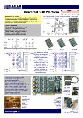
PCI
HOST
Interface
PCI
BUS
FPGA
LOGIC and DSP
resource
MCU
Config
EEPROM
Control
EEPROM
PROM
JTAG
FPGA
JTAG
Dedicated
data
connection
RS-232
serial control
interface
Front-end
BUS
Control
BUS
CLK DRV
/2, /4
X2, X4SCLK
OSC
External
CLK in/out
LCLK
OSC
Sampling
CLK
Local
CLK
I2C
FPGA CFG
Clock
lines
Different
front-end
configurations
External
TRG in/out
The SDR card family is based on feature-reach PCI base board:
14-Bit
ADC
(AD6644)
Clocking
and
Timing
Cross
Connect
Switch
(CPLD)
Cross
Connect
Switch
(CPLD)
Cross
Connect
Switch
(CPLD)
Cross
Connect
Switch
(CPLD)
Digital
Receive
Processor
(AD6624)
Digital
Receive
Processor
(AD6624)
Digital
Receive
Processor
(AD6624)
Digital
Receive
Processor
(AD6624)
Local
DSP
and
Data
Routing
Resource
(Xilinx
FPGA)
HOST
Interface
(PLX9054)
PCI
Bus
RCh1
RCLK
Config
Control
TRG
DRU-204
Dedicted
Data ports
14-Bit
ADC
(AD664)
14-Bit
ADC
(AD6644)
14-Bit
ADC
(AD6644)
14-Bit
ADC
(AD6644)
Clocking
and
Timing
Cross
Connect
Switch
(CPLD)
Cross
Connect
Switch
(CPLD)
Cross
Connect
Switch
(CPLD)
Cross
Connect
Switch
(CPLD)
Digital
Receive
Processor
(AD6624)
Digital
Receive
Processor
(AD6624)
Digital
Receive
Processor
(AD6624)
Digital
Receive
Processor
(AD6624)
Local
DSP
and
Data
Routing
Resource
(Xilinx
FPGA)
HOST
Interface
(PLX9054)
PCI
Bus
RCh1
RCh2
RCh3
RCh4
RCLK
Config
Control
Dedicted
Data ports
TRG
DRU-204
One of the main feature
of the converter cards is
the programmable
universal cross-connect
switch.
Using these connection
elements the signal can
be routed to form
multidrop multichannel
(up to 16ch/board) or
phased array (up to
4ch/board) receiver or
transmitter board.
Link port or
serial port can
be used for
real-time data
connection to
the DSP
Technology enhancements include:
•Up to 80MHz sampling clock
•270MHz input bandwidth
•Slot card or stand alone operation
•Control trough the PCI or on-board uC
•FPGA firmware booting trough PCI or by uC
•Using master mode PCI interface chip
•Local bus logic implementation in FPGA
•On-board Digital Down Conversion chips
•External connection (link, serial) to DSP
•Multifunctional triggering IO
•Internal or external clocking
Type Analog
input
channels
Analog
input
BW
ADC Input
sample
FIFO
DDC Analog
output
channel
s
Analog
output
BW
DAC Output
sample
FIFO
DUC
DIU-202 2 250
MHz
14bit
65MHz
2KW-
65KW
-
DOU-202 2 300
MHz
14bit
80MHz
2KW-
65KW
-
DCU-202 1 250
MHz
14bit
65MHz
2KW-
65KW
- 1 300
MHz
14bit
80MHz
2KW-
65KW
-
DCU-204 2 250
MHz
14bit
65MHz
2KW-
65KW
- 2 300
MHz
14bit
80MHz
2KW-
65KW
-
DRU-204 4 250
MHz
14bit
65MHz
- 16ch
DTU-204 4 300
MHz
14bit
80MHz
- 16ch
DCU-204 DRU-204 DTU-204
Typical
integrated
SDR platform
based on
Pentium SBC,
Sharc DSP,
DRU-204
converter
and FCU
Frequency
conversion unit
is implemented
as typical
analog RF
signal
processing
hardware
element