Wide linear range OTA
•Als PPTX, PDF herunterladen•
0 gefällt mir•621 views

Wide linear range operational trans conductance amplifier design for ultra low power applications

Empfohlen
Weitere ähnliche Inhalte
Was ist angesagt?
Was ist angesagt? (20)
Ähnlich wie Wide linear range OTA
Ähnlich wie Wide linear range OTA (20)
Kürzlich hochgeladen
Kürzlich hochgeladen (20)
Wide linear range OTA
- 1. 1
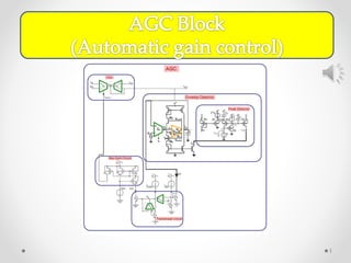
- 2. 1st AGC • The AGC compresses this input Dynamic range from 77dB to a narrower 57-dB internal dynamic range (IDR) at which each of the 16 channels of the processor operate. • Implementation: -The AGC circuit of the processor is implemented by regulating the trans conductance of a simple trans conductance-resistance variable gain amplifier (VGA). A=Gm1*R=Gm1*Gm2 • How to regulate (control) : • Using the Trans-linear compression circuit : Used to decreases the gain current to the VGA as the envelop level of the output signal increases (controlled by Iref & Ied) 2
- 3. 1st AGC cont’ -A current Ig, proportional to Ln 𝐼𝑖𝑛 𝐼𝑟𝑒𝑓 ,is output by the trans conductance amplifier with bias current I1 -Ig converted to a voltage on the effective load resistance G2 created by the trans conductance amplifier with bias current I2 . -The voltage Vg is exponentiated by the output transistor to Create Iout , which is conveyed through a cascode transistor and current mirror to create Icontrol . 3
- 4. Maximum gain circuit • A minimum-current circuit enforces a maximum gain by comparing the gain current Imax with Igain and switching the smaller of the two to the VGA. 4
- 5. WLR • Why we need a WLR? 1st: :The constant range means a constant gain. 2nd: The linear range means that the gain is variable but increases linearly. • How to obtain a WLR? • The trans-conductance output shape is a tanh curve. Then we can obtain WLR by 1- winding the tanh . 2- or decreasing the ratio of trans-conductance to bias current . • Used topologies: 1. Feed-back technique of emitter degeneration. 2. Fifth order technique. 3. Trans-linear circuit and a resistor technique. 4. Bi-CMOS trans-conductor technique. 5. Our novel technique. 5
- 6. WLR cont’ Can we use a simple differential pair? NO we can’t such that the linear range of it extends to only 75mv (a very low range) Then we need to make improvements in the known differential pair circuit to increase its linear range. 6
- 7. The novel technique. -This method uses a combination of four techniques to improve the differential-pair transistor : a. Well terminals of the input differential-pair transistors are used as the amplifier inputs. b. Source degeneration. c. Gate degeneration. d. Bump-linearization. 7
- 8. The novel technique cont’ a- Why we choose the well to be an input terminal ? -Then if K>0.5( which is almost always the case)then the well trans-conductance has a lower magnitude than the gate trans-conductance, and the well is preferable over the gate as a low-trans-conductance input. Degradation: Since Gm = 𝐼𝑠 𝑉𝑡 Then Gm α Is 8
- 9. The novel technique cont’ b- What is the idea behind source degeneration? • The idea behind source degeneration is to convert the current flowing through a transistor into a voltage through a resistor or diode, and then to feed this voltage back to the source of the transistor to decrease its current. c- What is the idea behind gate degeneration? • The idea behind gate degeneration is to convert the current flowing through a transistor into a voltage through a diode, and then to feed this voltage back to the gate of the transistor to decrease its current. • There are another function of this technique The gate-degeneration diode is essentially free in our circuit, because it is part of the current mirror that feeds the differential- arm currents to the output. 9
- 10. The novel technique cont’ 10
- 11. The novel technique cont’ d-Bump linearization: • it is a technique for linearizing a tanh and extending the linear range of the differential pair. • Since the region near the origin is linear (at low currents) • Then we will use a combination of two series transistors to steel current from the differential pair output. • Due to experiment it found that the maximum linear range found at 𝑊 𝐿 = 2 . 11
- 12. The novel technique cont’ • The experimental data: Due to all the previous techniques and after adding the current mirror biasing circuit (whose transistors mentioned by M) we found: 12