3-D imaging by terahertz scanner
•
1 gefällt mir•457 views

With the recent development of improved 3D imaging, ARP’s terahertz scanner is now capable of “seeing” inside of wafers and image defects. Thus, in addition to quantifying the defect size, one is also able to visualize the defects on the nanometer scale.

Empfohlen
Empfohlen
Weitere ähnliche Inhalte
Mehr von Applied Research and Photonics, Inc.
Mehr von Applied Research and Photonics, Inc. (20)
Kürzlich hochgeladen
Kürzlich hochgeladen (20)
3-D imaging by terahertz scanner
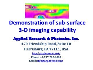
- 1. Demonstration of sub-surface 3-D imaging capability Applied Research & Photonics, Inc. 470 Friendship Road, Suite 10 Harrisburg, PA 17111, USA http://arphotonics.net/ Phone: +1-717-220-1003 Email: info@arphotonics.net
- 2. Demonstration of sub-surface 3-D imaging capability With the recent development of improved 3D imaging, ARP’s terahertz scanner is now capable of “seeing” inside of wafers and other opaque substrates. A scanning image is generated pinpointing location and size of particulate, void, and other defects. In addition, defect size is quantified by to-the- scale direct measurements. It can also visualize the defects on the nanometer scale.
- 3. Snap shot of patterns on a wafer Scanned surface image of a wafer. Total scan length is ~5 µm.
- 4. 360° inside view of the object 360° view of a wafer. Color contrast represents objects of different size and material.
- 5. Scanner details • The terahertz sub-surface scanner from ARP is a user friendly, easy to use machine. • All operations are automated via included software. • The machine exhibits an unprecedented resolution of a few nanometers in 3 axial directions. • Yet scanning is fast
- 6. Scanner details (contd.) • Screen shot of measurement console shown in the next slide. • All parameters are entered by the front- end interface. • Measured data are accessible for further manipulations.
- 7. Measurement Console Screen shot of measurement console. All parameters are entered via the front-end. Data are easily accessible.
- 8. Contact information For more information, please contact: Anis Rahman, PhD email: info@arphotonics.net Phone: 717-623-8201