Flipchip Technologies & Market Trends 2015 Report by Yole Developpement
•
8 gefällt mir•11,567 views

Flipchip Technologies & Market Trends Flip chip More information on that report at http://www.i-micronews.com/reports.html

Empfohlen
Empfohlen
Weitere ähnliche Inhalte
Was ist angesagt?
Was ist angesagt? (20)
Ähnlich wie Flipchip Technologies & Market Trends 2015 Report by Yole Developpement
Ähnlich wie Flipchip Technologies & Market Trends 2015 Report by Yole Developpement (20)
Mehr von Yole Developpement
Mehr von Yole Developpement (20)
Kürzlich hochgeladen
Kürzlich hochgeladen (20)
Flipchip Technologies & Market Trends 2015 Report by Yole Developpement
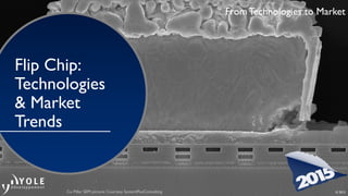
- 1. From Technologies to Market Flip Chip: Technologies & Market Trends From Technologies to Market © 2015Cu Pillar SEM picture: Courtesy SystemPlusConsulting
- 2. 2 Biography & contact ©2015 | www.yole.fr | Flip Chip Report 2015 Thibault Buisson Santosh Kumar Santosh Kumar is currently working as Senior Technology & Market Research Analyst at Yole Développement. He worked as senior R&D engineer at MK Electron Co. Ltd where he was engaged in the electronics packaging materials development and technical marketing. His main interest areas are advanced electronic packaging materials and technology including TSV and 3D packaging, modeling and simulation, reliability and material characterization, wire bonding and novel solder materials and process etc. He received the bachelor and master degree in engineering from the Indian Institute of Technology (IIT), Roorkee and University of Seoul respectively. He has published more than 20 papers in peer reviewed journals and has obtained 2 patents. He has presented and given talks at numerous conferences and technical symposiums related to advanced microelectronics packaging. Contact: kumar@yole.fr Thibault Buisson is currently working as Technology and Market Research Analyst in the Advanced Packaging team at Yole Développement. He graduated from INPG with a Master of Research in Micro and Nano electronics and from Polytech’ Grenoble with an engineering degree in Material Sciences. He then joined NXP Semiconductors as R&D process engineer in the thermal treatment area to develop CMOS technology node devices from 65 to 45nm. Afterwards, he joined IMEC Leuven and worked for more than 5 years as process integration engineer in the field of 3D technology. During this time, he has worked on several topics from TSV to micro-bumping and stacking. He has authored or co-authored fifteen international publications in the semiconductor field and given talks at several conferences and technical symposiums. Contact: buisson@yole.fr
- 3. 3©2015 | www.yole.fr | Flip Chip Report 2015 WHAT IS NEW? • Updated market capacity and wafer forecast from 2014 to 2020 • Flip Chip players and 2014 ranking. • Recent M&A • Technology roadmap for Flip Chip bumping • Updated information for Flip Chip on devices and applications • Focus on LEDs and CMOS image sensors
- 4. 4©2015 | www.yole.fr | Flip Chip Report 2015 TABLE OF CONTENT Part 1/2 I. Introduction, Definitions & Methodology-----------------------------------------------------------2 • Glossary • Report Objectives • Who should be interested in this report • Companies cited in the report • Methodology II. Executive Summary-------------------------------------------------------------------------------------15 III. Flip Chip Technology-----------------------------------------------------------------------------------37 • Packaging and Interconnections Trends • Technology (Flip Chip) Roadmap IV. Flip Chip Players----------------------------------------------------------------------------------------52 • Geographical locations of Flip Chip Players • Repartition of FC players • Players manufacturing Au Stud bumps • Players manufacturing Au ECD bumps • Players manufacturing Solder Bump • Players manufacturing Cu Pillar IV. Flip Chip Market update-----------------------------------------------------------------------------60 • Market drivers • Players Ranking by wafer capacity • All Players • Cu Pillar players • ECD Players • Au ECD Players • Au Stud bump Players • Au bumping • Au bumping drivers • Flip Chip Au ECD bump capacity forecast – breakdown by players • Flip Chip Au ECD bump capacity share – breakdown by players • Flip Chip Au ECD bump capacity – breakdown by business model • Flip Chip Au ECD – summary IV. Flip Chip Market update • Au bumping • Flip Chip Au stud bump capacity forecast – breakdown by players • Flip Chip Au stud bump capacity share – breakdown by players • Flip Chip Au stud bump capacity – breakdown by business model • Flip Chip Au stud – summary • Flip Chip Au (stud + ECD) bump capacity forecast – breakdown by players • Flip Chip Au (stud + ECD) bump capacity share – breakdown by players • Flip Chip (Au+ECD) stud – summary • Solder bump • Flip Chip solder bump capacity forecast – breakdown by players • Flip Chip solder bump capacity share – breakdown by players • Flip Chip solder bump capacity – breakdown by business model • Flip Chip solder bump – summary • Samsung Galaxy S6 teardonw PoP Package teardown • AMD graphic card radeon R9 Fury X package teardown • Cu Pillar • Flip Chip copper pillar capacity forecast – breakdown by players • Flip Chip copper pillar capacity share – breakdown by players • Flip Chip copper pillar capacity – breakdown by business model • Flip Chip copper pillar – summary • Flip Chip Market • FC Bump capacity forecast – summary • FC capacity forecast – breakdown by FC technology • FC Wafer start expected • FC bump capacity vs demand • Market segments • FCIP and Chip on Board • FC Forecast – breakdown by market segment • FC Forecast – breakdown by IC type • FC Units shipment forecast • FC Market value
- 5. 5©2015 | www.yole.fr | Flip Chip Report 2015 TABLE OF CONTENT Part 2/2 IV. Flip Chip Market update • Flip Chip Market • FC bump capacity – breadkown by business models • FC makert – Key figures! • Focus on LED-----------------------------------------------------------------------------121 • Focus on CIS------------------------------------------------------------------------------149 V. Recent Headlines-------------------------------------------------------------------------------------156 • Capacity increase / M&A / joint ventures • Comments on recent press releases VI. Supply Chain------------------------------------------------------------------------------------------160 • Flip Chip supply chain • Supply chain cases • Quaclomm case • AMD case • TI case • Intel Case • Sony for CIS • Comments on the supply chain VII. Assembly Technology----------------------------------------------------------------------------170 • Substrate • Underfills • Flip Chip Bonders • Thermal Interface Materials • Alternative to FlipChip VIII. Conclusion------------------------------------------------------------------------------------------234 • Summary • Future perspectives Appendix VIII. Flip Chip Definitions and Process Flows-------------------------------------------------------239 • FC Definition • FC Process flow • FC Overview • Under Bump Metallization Definition • Difference between FC and WLCSP • Bumping hierarchy in FC – 3D/2.5D case • ECD solder and Au plated bump • Electroplated bump deposition • C4 Bump • Cu pillar • Au ECD bump process flow • Cu Pillar • Au stud bumping • Stud bumping definition • Stud bumping process flow IX. Yole Presentation--------------------------------------------------------------------------------------269
- 6. 6©2015 | www.yole.fr | Flip Chip Report 2015 REPORT OBJECTIVES The objectives of this report are: • To provide analysis and understanding of Flip Chip markets, player dynamics and key trends • To provide market data on Flip Chip capacity forecasts in wafer starts and $M for 2014–2020. • To identify future Flip Chip strategy evolution and opportunities • To provide an overview of Flip Chip technology and trends
- 7. 7©2015 | www.yole.fr | Flip Chip Report 2015 COMPANIES CITED IN THE REPORT AMD, AMKOR TECHNOLOGY, APPLE, ASE, GROUP, ATP, AT&S, CARSEM, CHINA WLCSP, CHIPBOND, CHIPMOS, CITIZEN, COWELL, CREE, E-SILICON, EDISEN-OPTO, ELEC-TECH, EPILEDS, EPISTAR, EVERLIGHT, FIRST LEVEL INC, FLIP CHIP INTERNATIONAL, FORMOSA EPITAXY, FREESCALE, GENESIS PHOTONICS, GLOBALFOUNDRIES, HC SEMITEK, HONGLITRONICS, IBIDEN, IBM, ILIJN LED, INARI TECHNOLOGY, INTEL, IPDIA, J-DEVICES, JCET, KUNSHAN HUATIAN, LBSEMICON, LEXTAR, LG INNOTEK, LUMENS, LUMILEDS, LUMEX, MICRON, MURATA, NEPES, NICHIA, NYPCB, OPEN- SILICON, OPTOCAP, ORIENT SEMICONDUCTOR, OSRAM, PACTECH, PANASONIC CORPORATION, POWERTECH TECHNOLOGY, PRIMAX, QUALCOMM, QUIK-PAK, RENESAS, SAMSUNG ELECTRONICS, SANAN, SEMCO, SEMCO- WISOL, SEMILEDS, SHARP, SHINKO, SIGNETICS, SK HYNIX, SMIC, SONY, SPIL, STATSCHIPPAC, STMICROLECTRONICS, TAIYOYUDEN, TEKCORE,TEXAS INSTRUMENTS,THEIL,TRIQUINT,TSMC, UNIMICRON, UNISEM… and more
- 8. 8©2015 | www.yole.fr | Flip Chip Report 2015 WHO SHOULD BE INTERESTED IN THIS REPORT? o OSAT, IDMs, foundries companies: • To have a broad overview Flip Chip applications & markets • To identify new markets • To monitor and benchmark potential competitors o Financial & Strategic investors: • To understand the potential for Flip Chip technology. • To know the latest M&A • To get a list of Flip Chip players and their activities o R&D players: • To understand new technical challenges in Flip Chip technology o Equipment & Material suppliers: • To understand the technical evolution of Flip chip bumps. • To identify business opportunities and prospects o OEMs & Integrators: • To evaluate benefits of using Flip chip technology in systems
- 9. 9©2015 | www.yole.fr | Flip Chip Report 2015 The semiconductor industry is facing a new era: • FEOL transistor scaling and cost reduction will not continue on the same path they followed for the past few decades, with Moore’s law in its foundation • Advanced technology nodes do not bring the desired cost benefit anymore and R&D investments in new lithography solutions and devices below 10 nm nodes are rising substantially • New market shifts are expected in due time, with “Internet ofThings” getting ready to take over pole market driver position from mobile THE GROWTH OF ADVANCED PACKAGING Why Advanced Packaging? Advanced packaging is transitioning to high-performance,high-density,low-cost collective wafer level packaging techniques. • While FEOL scaling options remain uncertain and IoT promises application diversification, the spotlight is now turned to advanced packages for: • Cost reduction • Performance boost • Functionality boost • In order to answer market demands, the advanced packaging segment focuses on integration and wafer level packages Mobile ©2015 | www.yole.fr | Fan-in WLP: Market and Technology Trends Flip chip BGA type of package
- 10. 10©2015 | www.yole.fr | Flip Chip Report 2015 Surface Mount Ball grid arrays SiPs Fan-inWLP FC BGA PoP More SiPs Interposers 3D IC TSV FO WLP 1980 Packaging technology evolution GapFeaturesSivsPCB Through hole Increase in Packaging Technology Solutions Flip Chip is a key Technology MICROELECTRONICs PACKAGE EVOLUTION Mature 1970 1990 2000 2010 DIP, PGA SOP, QFP, PLCC CSPs/BGAs Today Established Emerging Feature sizes of PCBs Feature sizes CMOS Bridging the Gap Between Si and PCB Processing Capabilities ©2015 | www.yole.fr | Fan-in WLP: Market and Technology Trends
- 11. 11©2015 | www.yole.fr | Flip Chip Report 2015 SILICON / INTERCONNECTION TREND Transistor scaling will not continue on the same path, alternatives are sought for cost reduction 500 020406080100 20.000 10.000 1500 CMOS90 CMOS45 CMOS28 CMOS14CMOS65 FinFET CMOS Tech. Node [nm] Transistor scaling and cost reduction will not continue on the same path – reaching sub 10nm grey zone 10 Cost reduction vs. Technology opportunities I/O per cm² WHAT ARETHE OPTIONS? • Continue with development of advanced technology nodes (follow Moore’s Law) • Develop new alternative technologies/packages (More than Moore) to meet the market requirements ©2015 | www.yole.fr | Fan-in WLP: Market and Technology Trends
- 12. 12©2015 | www.yole.fr | Flip Chip Report 2015 FLIP CHIP MARKET DRIVERS CPUs / GPUs/chipsets, the earlier adopters of flip chip packaging, continue to grow at steady rate • Almost all central processor units (CPUs), graphical processor units (GPUs) and chipsets are packaged using flip-chip. e.g, all CPUs & GPUs Intel,AMD & Nvidia • CPUs and chipsets are mainly packaged in fcLGA (land grid array) and GPUs in fcBGA format. • The main benefit that drive the use of flip chip for these devices are high I/Os, large chip to package area, superior electrical and thermal performance. chipsets
- 13. 13©2015 | www.yole.fr | Flip Chip Report 2015 FLIP CHIP MARKET DRIVERS Benefits provided by flip chip technology drive its adoption across various segments APE CPU GPU BB PMU RF FPGA DD Memory ASIC CIS LED High I/O density Large chip to package area Fine pitch interconnection Electrical performance Thermal dissipation Ergonomics, topology Flip chip assembly technology provide various benefits such as high I/Os, fine pitch interconnection, superior electrical and thermal performance which drives its applications across specific segments as seen below. -DD is display driver -CIS is CMOS image sensor -BB is baseband processor -PMU is power management unit More details in the report
- 14. 14©2015 | www.yole.fr | Flip Chip Report 2015 PACKAGING TRENDS From standard package types to advanced packages With the number of I/O constantly increasing Flip Chip is a key Technology! 2000mm² FOOTPRINT I/O64 144 500 1531 3000 3000mm² 1000mm² 20mm² FCBGA 55*55mm FCBGA 40*40mm FCBGA 31*31mm PBGA 27*27mm LFBGA 17*17mm BGA 15*15mm SO BGA 10*10mm QFP WLCSP WIRELESS COMMUNICATION COMPUTING/ NETWORKING CONSUMER FCBGA Substrate Build-Up SubstratesLaminate SubstratesLead-frame FCCSP Hybrid FCCSP/FCBGA
- 15. 15©2015 | www.yole.fr | Flip Chip Report 2015 FLIP CHIP TECHNOLOGY ROADMAP Current 2016 2017 20192018 2020 ≤ 32nm 28nm 14nm Siliconnode 10nm Sn-Pb Lead free Cu Pillar Bumping Technology MetallurgyPitch Au bump >150um 40-150um <40um Bump Height Solder Cu pillar More details in the report
- 16. 16©2015 | www.yole.fr | Flip Chip Report 2015 FLIP CHIP BUMP CAPACITY FORECAST Breakdown by Flip Chip Technology 26M 12’’eq wafers capacity in 2020! • Cu Pillar will take market share from the others flip chip technology • Wafer capacity forecast will increase from 16M in 2014 up to 26M in 2020 • 9% CAGR expected for bumping capacity - 5 000 000 10 000 000 15 000 000 20 000 000 25 000 000 30 000 000 0% 10% 20% 30% 40% 50% 60% 70% 80% 90% 100% 2014 2015 2016 2017 2018 2019 2020 WaferCounrt[12"eq.wspy] 2014-2020 Flip Chip Bump Capacity Forecast Breakdown by Flip ChipTechnology (12''eq. wspy) Cu Pillar Au (ECD+Stud) ECD Solder Total Note: CIS and LED not included
- 17. 17©2015 | www.yole.fr | Flip Chip Report 2015 FLIP CHIP TECHNOLOGY Accross different Market Segment …And much more! Consumer Automotive Medical Industrial Mobile/wireless Computing Smartphones Tablets Laptops UHDTV Game Station Desktop PC Set-up Box Cars Ultrasonic Handler Servers
- 18. 18©2015 | www.yole.fr | Flip Chip Report 2015 SAMSUNG GALAXY S6 Processor Package Teardown Solder Bumping used for flip chip of the process in the Samsung Galaxy S6 Samsung Exynos 7420 + K3RG3G30MM-DGCH Solder bump used to stack the processor onto the organic substrate Courtesy System+Consulting Courtesy System+Consulting
- 19. 19©2015 | www.yole.fr | Flip Chip Report 2015 OSAT 36% IDM 26% IC Foundry 11% Bumping House 27% OSAT 41% IDM 28% IC Foundry 10% Bumping House 21% 2014 - 2020 Flip Chip Bump Capacity Breakdown by business model (12''eq. wspy) FLIP CHIP BUMP CAPACITY Breakdown by Business Models including all type for Flip Chip Bumps OSAT & IDM are the key business models for flip chip technology • OSATs are the leading business model for flip chip bumps with 36% of the wafer capacity followed by bumping houses and IDMs with respectively 27% and 26% • IC foundry business model has the smallest percentage with only 11% of the wafer capacity • OSATs will continue to grow up to 41% in wafer capacity in 2020 whereas IC foundry and bumping houses will decrease in wafer capacity • IDMs will also continue to gain share in wafer capacity up to 28% in 2020 2020 2014
- 20. 20©2015 | www.yole.fr | Flip Chip Report 2015 FLIP CHIP PLAYERS IN LED Key Players Identified Majority of players are located in Asia (Taiwan, Korea & China) Lumileds, Lumex, CREE Osram1 Lumens, Iljin LED, Samsung, LG Nichia, Citizen Genesis Photonics, Everlight, Epistar, Formosa Epitaxy2, Lextar, Epileds, TSMC, Edison Opto, Tekcore, SemiLEDs Elec-Tech, Sanan, APT, HC Semitek, Honglitronics • 1. Osram use its UX:3 thin-film flip-chip manufacturing platform however the technology is much more similar to vertical LED technology than Flip Chip LED technology. • 2. Formosa Epitaxy was Acquired by Epistar in July 2014. During our analysis, we were not able to identify any involvement from Sharp, Optogan or Citizen Electronics in Flip Chip product development and / or commercialization.
- 21. 21©2015 | www.yole.fr | Flip Chip Report 2015 CIS: IPHONE6 CAMERA MODULE TEARDOWN Au stud bump on ceramic substrate!
- 22. 22©2015 | www.yole.fr | Flip Chip Report 2015 TOP PLAYERS IN 2014 Flip chip assembly #1 players 2014 (#1player ) Bumping & Assembly location TAIWAN Advanced Underfill HENKEL Flip chip bonder BESI Solder ECD bumping SPIL Gold bumping ChipBOND Cu pillar bumping INTEL Top Players
- 23. © 2015 Yole Développement FromTechnologies to Market
- 24. 24 MEMS & Sensors LED Compound Semi. Imaging Photonics MedTech Manufacturing Advanced Packaging PV Power Electronics FIELDS OF EXPERTISE Yole Développement’s 30 analysts operate in the following areas ©2015 | www.yole.fr | Name of the report
- 25. 25 4 BUSINESS MODELS o Consulting and Analysis • Market data & research, marketing analysis • Technology analysis • Strategy consulting • Reverse engineering & costing • Patent analysis www.yole.fr o Reports • Market & Technology reports • Patent Investigation and patent infringement risk analysis • Teardowns & Reverse Costing Analysis • Cost Simulation Tool www.i-Micronews.com/reports o Financial services • M&A (buying and selling) • Due diligence • Fundraising • Maturation of companies • IP portfolio management & optimization www.yolefinance.com www.bmorpho.com o Media • i-Micronews.com website • @Micronews e-newsletter • Technology magazines • Communication & webcast services • Events www.i-Micronews.com ©2015 | www.yole.fr | Name of the report
- 26. 26 A GROUP OF COMPANIES Market, technology and strategy consulting www.yole.fr M&A operations Due diligences www.yolefinance.com Fundraising Maturation of companies IP portfolio management & optimization www.bmorpho.com Manufacturing costs analysis Teardown and reverse engineering Cost simulation tools www.systemplus.fr IP analysis Patent assessment www.knowmade.fr ©2015 | www.yole.fr | Name of the report
- 27. 27 OUR GLOBAL ACTIVITY Yole Japan Yole Inc. Yole Korea 40% of our business is in EU countries 30% of our business is in North America 30% of our business is in Asia ©2015 | www.yole.fr | Name of the report
- 28. 28 SERVING THE ENTIRE SUPPLY CHAIN Our analysts provide market analysis, technology evaluation, and business plan along the entire supply chain Integrators and end-users Device makers Suppliers: material, equipment, OSAT, foundries… Financial investors, R&D centers ©2015 | www.yole.fr | Name of the report
- 29. 29 CONTACT INFORMATION o Consulting and Specific Analysis • North America: Steve LaFerriere, Business Development Manager,Yole Inc Email: laferriere@yole.fr • Japan:Yutaka Katano, General Manager,Yole Japan & President,Yole K.K. Email: katano@yole.fr • RoW: Jean-Christophe Eloy, President & CEO,Yole Développement Email: eloy@yole.fr o Report business • North America: Steve LaFerriere, Business Development Manager,Yole Inc Email: laferriere@yole.fr • Europe: Jérôme Azemar, Business Development Manager, European Office Email: azemar@yole.fr • Japan & Asia:Takashi Onozawa, Sales Asia & General Manager,Yole K.K. Email: onozawa@yole.fr • Korea: HaileyYang, Business Development Manager, Korean Office Email: yang@yole.fr o Financial services • Jean-Christophe Eloy, CEO & President Email: eloy@yole.fr o General Follow us on ©2015 | www.yole.fr | Name of the report