SlideShare ist ein Scribd-Unternehmen logo
1 von 9
Downloaden Sie, um offline zu lesen
Standardized Direct Charge Device ESD Test For
Magnetoresistive Recording Heads I
Tim Cheung (2), Lydia Baril (1), Albert Wallash (1)
(1) Maxtor Corporation, 500 McCarthy Blvd, Milpitas, CA 95035 USA
Tel.: 408-324-7067, fax: 408-894-3207, e-mail: lydia_baril@maxtor.com
(2) Previously at ReadRite Corporation, 44100 Osgood Rd, Fremont, CA 94359 USA
Tel: 805-967-8152, email: tocheung2u@yahoo.com
Abstract – The effects of the Human Body Model (HBM) Electrostatic Discharge (ESD) waveform on Giant
Magnetoresistive (GMR) recording heads is well characterized. This information has provided a starting point
for understanding ESD damage to magnetic recording heads but the HBM no longer reflect the reality of ESD
mechanisms along the production lines. Damage will most likely occur from metal contact to the MR
electrodes (metal) rather than from bare fingers. Direct Charged Device Model (DCDM) can be used to
simulate metal-to-metal contact discharge. A manual DCDM was characterized using disk capacitors. DCDM
manual ESD testing of grounded (suspension is grounded) and floating suspension (suspension is not connected
to ground) GMR heads was performed, and a DCDM breakdown voltage ranging from 3V to 9V was measured.
Pspice simulation was used to simulate the DCDM discharging events, the results agree well with the DCDM
manual discharge data.
I. Introduction
It is well known the GMR heads are sensitive to
damage from an electrostatic discharge (ESD) event,
as the areal density increases dramatically in magnetic
recording industry, the magnetic recording heads
become more susceptible to electro-overstress (EOS),
and electrostatic discharge (ESD) events. HBM no
longer reflects the reality of ESD damage along the
manufacturing lines. ESD will mostly occur from
direct charging the GMR head capacitances then
followed by metal contact to an input, MR+ or MR-,
of a GMR head. ESD damage to GMR heads during
all stages of handling and assembly is a serious
problem in magnetic recording head manufacturing.
The GMR sensor will have a voltage if the sensor is
itself charged, or if it is in the electric field of a
nearby, charged insulator. Tribocharging during
handling of a head gimbal assembly (HGA) with an
insulating Kapton flex circuit has often been the root
cause of severe ESD problems. ESD testing that
directly charges and then grounds the MR+ or MR- of
a GMR head, known as “DCDM” shows that if the
GMR sensor at about 4V is grounded, then the current
that flows through the GMR sensor is severe enough
to change the sensor resistance. The discharge current
waveform from metal contact and DCDM to a GMR
head are similar. The purpose of this paper is to
characterize the DCDM and understand how the
system behaves using disk capacitors, GMR heads,
and Pspice simulations.
II. Experimental Setup
The experimental setup consisted of the following
components:
1) Manual DCDM test jig
2) Tektronix CT-6 current probe
3) Tektronix 3GHz TDS694C Digital Oscilloscope
4) HP Digital Control Power Supply
5) Gold plated metal plate
6) Disk capacitors
Figure 1a. Schematic representation of the DCDM manual test jig
for disk capacitors.
High Speed
Oscilloscope
+ GND
10MCT-6
Ground Plate
Short Wire
Power Supply
Disk
Capacitor
The purpose of using a manual test jig is that it has
very small parasitic capacitance and inductance.
Figure 1a shows the schematic representation of
DCDM manual test jig. The inductanceless disk
capacitors are made out of 0.8 mm thick FR-4 double-
sided printed circuit board (PCB). One side of the
board is gold-plated etched to a circular disk, and the
other is gold-plated ground plane. The capacitance
depends on the size of a circular disk (the spacing is
fixed). The larger the circular disk is the higher the
capacitance. Figure 1b shows four different sizes of
disk capacitance, 0.5pF, 2.2pF, 4.4pF, and 11.5pF.
Figure 1b. Four disk capacitors 0.5pF, 2.2pF, 4.4pF and 11.5pF.
Figure 1c. DCDM manual test jig for disk capacitors.
The bottom plate of the capacitor lies on a grounded
gold-plated metal. The grounded metal plate is gold-
plated for good contact between the bottom plate of
disk capacitor and metal plate. A voltage source
provides voltage to the top plate of the disk capacitor
through a 10MΩ resistor. The voltage source is
continuously charging the disk capacitor. A short
wire of about half inch long is connected to a
grounded metal plate through a CT-6 current probe
(See Figure 1c). The disk capacitor surface and the
grounded wire must be cleaned. The discharge of the
disk capacitor is done manually contacting one end of
the ground wire to the top disk plate. During
discharge process, the manual contact must be very
fast and precise. The discharge current waveforms are
detected with a CT-6 current probe and the
waveforms are captured from a high-speed digital
oscilloscope Tektronix TDS 694C 3GHz and 10GS/s.
Figure 2 shows that the grounded and floating
suspension GMR heads were tested on the same
DCDM manual test jig. A grounded suspension HGA
means that the suspension contacts the grounded
metal plate. A floating suspension HGA means that
the suspension is isolated from the grounded metal
plate. A 10MΩ resistor is connected from a power
supply to the MR+ of a GMR head. Then, the
grounded short wire contacts the MR+ or MR- pad for
discharge the charged GMR head. The CT-6 current
probe captures the discharge current; the high speed
oscilloscope is used to monitor the discharge current,
and an Ohmmeter is used to measure the MR
resistance after each discharge event until the MR
resistance changed more than 1%. (Note: Use the MR
resistance failure for reference only, magnetic
performance is more susceptible to ESD damage).
Figure 2. Schematic representation of the DCDM manual test jig
for GMR head.
III. Experimental Results and
Analysis
Figure 3 shows a simplified electrical equivalent
circuit for DCDM manual test jig. The voltage source
is not shown in the circuit. Cdisk is the disk capacitor,
L1 is the inductance of the grounded wire, Cp is the
parasitic capacitance of the circuit, Rspark is the spark
resistance, which is created during the grounded wire
contacts the charged disk capacitor.
High Speed
Oscilloscope
+ GND
10MCT-6
Metal Plate
Short Wire
Power Supply
HGA
10 MΩ resistor
CT6
Short wire
Power supply +
Ground
To Oscilloscope Metal plate
Figure 3. Electrical equivalent circuit for DCDM manual testing
for disk capacitor.
Figure 4 shows an example of discharge current
waveform for a disk capacitor 4.4pF at charging
voltage of 4V. The first peak current reaches 54mA
and the pulse width is about 0.47ns. There is a second
peak of opposite polarity or undershoot. Its peak
current level is about –21mA. Waveforms obtained in
the same manner for the same capacitance and the
same charging voltage is mostly reproducible, i.e.
peak current and pulse width values are within +/-
10%. Waveforms were captured for a range of
capacitor values and charging voltages.
Figure 4. Discharge current waveform of a 4.4pF disk capacitor at
4V.
Figure 5a shows the manual test discharge current for
four different capacitances and voltages. The
discharge current equation is given by:
)sin()( tetI t
L
V
ωα
ω
−
= (3)
where α = R/2L, ω = 2πf = ,
I(t) is the discharge current and V is the voltage on the
capacitor. The equation (3) shows that the voltage on
the capacitor is doubled, the discharge current is also
doubled. Figure 5b shows that the pulse width
decreases as the voltage on the capacitor increases.
The hypothesis for the decreasing pulse width at
higher voltage are the bandwidth limitation of a CT-6
current probe and the lower spark resistance as a
result of smaller change of time constant. Figure 5c
shows the discharge current saturated at high
capacitance. This is due to the smaller the
capacitance, the higher the discharge path impedance,
which limits the current. The magnitude of
impedance Z is given by:
,
where ω = 2πf, R is the equivalent resistance of the
inductor L1, the L is the inductance of the L1. Pspice
simulation will be used to verify this behavior.
Manual Charging/Discharging on Disk Capacitors
11.5pF y = 17.786x - 5.5478
4.4pF y = 12.151x - 3.4174
2.2pF y = 5.1043x + 0.0087
0.5pF y = 2.1426x + 0.3652
0
20
40
60
80
100
120
140
160
0 2 4 6 8 10
DCDM Voltage (V)
measuredIp(mA)
11.5pF
4.4pF
2.2pF
0.5pF
Figure 5a. Charging voltage versus discharge current for four
capacitors.
Manual DCDM 4.4pF @4V
-3.0E-02
-2.0E-02
-1.0E-02
0.0E+00
1.0E-02
2.0E-02
3.0E-02
4.0E-02
5.0E-02
6.0E-02
-1.E-09 0.E+00 1.E-09 2.E-09 3.E-09 4.E-09 5.E-09
Time (ns)
PeakCurrent(A)
Time (sec.)
Cdisk
Rspark
Cp
L1
SW
2
2
1
− ( )L
R
LC
( )22
LRZ ω+=
0.0
0.2
0.4
0.6
0.8
1.0
1.2
0 2 4 6 8 10
DCDM Voltage (V)
PeakWidthatHalfAmplitude(ns)
11.5pF
4.4pF
2.2pF
0.5pF
Figure 5b. Pulse width versus charging voltage for four
capacitances.
0
20
40
60
80
100
120
140
0 1 2 3 4 5 6 7 8 9 10 11 12 13
Capacitance (pF)
Ip(mA)
8V
4V
2V
1V
Figure 5c. Discharge current versus capacitance for four charging
voltages.
Figure 6 shows an electrical circuit model of the
DCDM manual testing for grounded suspension GMR
heads. The capacitance from the MR leads to
suspension is larger than other capacitance when the
suspension is grounded. The total capacitance of the
HGA depends on the type of flexcircuit. In this
particular flexcircuit HGAs, the total capacitance is
about 22pF from the MR leads to suspension. Figure
7 shows a simplified equivalent electrical circuit of
Figure 6. Where 22pF is the total head capacitance,
L1 is the total inductance of the MR lead and
inductance of discharge path.
Figure 6. Electrical circuit model of the DCDM manual testing for
grounded suspension GMR heads.
Figure 7. Simplified equivalent electrical circuit model for
grounded suspension GMR heads.
Figure 8 shows the discharge current of 51mA and the
pulse width of about 2ns at 4V for the grounded
suspension GMR head.
Figure 8. Discharge current waveform at 4V for grounded
suspension GMR head.
Figure 9 shows the electrical circuit model of the
DCDM, and the floating suspension GMR heads
(floating suspension means the suspension is not
connected to ground). The head capacitance is
dominated by the capacitance between the suspension
and the system ground.
Figure 9. Electrical circuit model of the DCDM and the floating
suspension GMR heads.
Manual DCDM: Grounded suspension
Criteria: MRR > 1%
-0.02
-0.01
0
0.01
0.02
0.03
0.04
0.05
0.06
-1.E-09 0.E+00 1.E-09 2.E-09 3.E-09 4.E-09 5.E-09 6.E-09 7.E-09 8.E-09 9.E-09
Time (ns)
Totaldischargecurrent(A)
breakdown at 4V
Time (sec.)
Rspark
L1
SW
CMR-to-grounded suspension 22pF
V
30nH30nH10nH
5pF 5pF
11pF
2pF
11pF
0.1pF
5pF
DCDM
MR
42Ω
1G
2Ω
10G
100G100G
Rsp
33Ω
1G
MR pad+ MR pad-
Bottom Shield
System Ground Substrate/Suspension
SW
V
10MΩ
2Ω
30nH30nH10nH
5pF 5pF
11pF
2pF
11pF
0.1pF
5pF
DCDM
MR
42Ω
1G
2Ω
10G
100G100G
40
1G
MR pad+ MR pad-
Bottom Shield
System Ground
Substrate/Suspension
SW
5pF 100G
V
10MΩ
2Ω
When the GMR head suspension is not grounded, the
capacitance from suspension to grounded metal plate
is approximately 5pF. Figure 10a shows the CMR-to-
suspension in series with the Csuspension-to-ground. The
total head capacitance can be calculated as follows:
C=(22pF)(5pF)/(22pF+5pF)=4pF
Figure 10a. Simplified electrical circuit model for a floating
suspension GMR head.
Figure 10b shows a simplified head capacitance from
MR-to-ground for floating suspension GMR head.
An equivalent head capacitance can be represented by
a single 4pF.
Figure 10b. Simplified electrical circuit model for a floating
suspension GMR heads with a total equivalent capacitance of 4pF.
Figure 11 shows the discharge current waveforms at
different charging voltages from 3V to 9V. The MR
resistance of this floating suspension head changed
from 42Ω to 54Ω at 9V breakdown. The peak current
amplitude at 9V is about 65mA, and the pulse width is
about 0.8ns.
Figure 11. Discharge current waveform at breakdown voltage of
9V for a floating suspension GMR head.
Figure 12 shows that the comparison of the
breakdown voltage for the grounded suspension and
the floating suspension GMR heads. The grounded
suspension heads were broken down at about 3V to
4V, and the floating suspension head was broken
down at about 9V at the GMR resistance changing
more than 1%. The floating suspension exhibits
higher breakdown voltage than the grounded
suspension GMR head because the grounded
suspension has a larger head capacitance than the
floating suspension GMR head reference to grounded
metal plate. The grounded suspension HGA has a
total head capacitance of about 22pF, and the floating
suspension HGA has a total head capacitance of about
4pF. The total head energy to damage to MR sensor
can be calculated and compared as follows:
For grounded suspension HGA:
A total head capacitance C of 22pF with a charging
voltage (V) at breakdown of 4V, then the total energy
can be calculated based on the equation:
E=1/2(C V 2
)=0.176nJ
For floating suspension HGA:
A total equivalent head capacitance C of 4pF with a
charging voltage (V) at breakdown of 9V, then the
total energy can be calculated based on the equation:
E=1/2(C V 2
)=0.162nJ
Comparing the two total energies, the floating
suspension HGA requires higher voltage to reach the
same energy level as for the grounded suspension
HGA that can damage the GMR sensor (assume same
MR resistance for both type). This is due to the
floating suspension HGA has lower head capacitance
than the grounded suspension HGA reference to
ground.
Csuspension-to-ground
CMR-to-suspension
Rspark
L1
SW
22pF
5pF
Rspark
L1
SW
4pF
V
CMR-to-ground
M a n u a l DCDM: Floating Suspension
-0.04
-0.02
0
0.0 2
0.0 4
0.0 6
0.0 8
-1.00E-09 0.00E+00 1.00E-09 2.00E-09 3.00E-09 4.00E-09 5.00E-09 6 .00E-09 7.00E-09 8.00E-09 9.00E-09
Tim e (ns )
Totaldischargecurrent(A)
3.05V 4V 4.5V 5V 5.5V 6 V 6.5 V 7V 7.5V 8V 8.5V 9 V 2.54V
Ip = 65mA @ 9V breakdown
PW50 = 0.8ns
Figure 12. GMR resistance versus DCDM breakdown voltage for
grounded and floating suspension GMR heads.
Discharge current occurs when the grounded wire is
brought near a charged disk capacitor, the electric
field between them increases to an extreme value.
When the field exceeds the dielectric breakdown
strength of air, current begins to flow by an avalanche
process. Eventually a low resistance spark develops.
The spark resistance can be affected by the contact
conditions such as humidity, contact speed, grounded
wire/disk capacitor plate material, the size and the
shape of the grounded wire tip and the contamination
between the grounded wire tip and the disk capacitor.
The following setup can be used for initial spark
resistance study.
Figure 13 shows the spark resistance test setup. A
low inductance surface mount resistor must be used.
The purpose of using additional resistance in series
with the discharge path is that the behavior of the
pulse width and the amplitude of the discharge current
can be observed. (See Figure 14)
Figure 13. Schematic representation of the spark resistance test
setup.
Figure 14 shows the discharge current waveforms
varying the different series resistances. The higher
the series resistance in the discharge path is the lower
the discharge current amplitude and wider the pulse
width. Both the resistance and impedance of the
inductor L1 in the discharge path can affect the
discharge current amplitude and the pulse wide.
The total resistance, Rt, in the discharge path is
approximately related by the following expression:
Rt = Rseries + Rspark + | Z | (4)
The magnitude of impedance Z is given by:
( )22 LRZ ω+= , (5)
where fπω = 2 , R is the equivalent resistance of the
inductor wire and L is the equivalent inductance, f is
the frequency. The Rspark and the impedance can be
calculated from the Equation (4):
Rspark + | Z | = Vc/Ip - Rseries
where Vc is the charging voltage on the capacitor, and
the Ip is the discharging current.
Figure 14. Discharge current versus Rseries at charging voltage
of 4V.
Figure 15 shows the Rspark and the impedance Z as a
function of charging voltage. The manual DCDM test
jig was used to perform this experiment (See Figure
13). The spark resistance plus the impedance Z
without adding the series resistance is 44Ω at 4V.
Based on the experimental data, the Rspark plus the
impedance Z increase as the charging voltage
decreases. However, we expected higher spark
resistance with the increasing of the charging voltage.
More experiments need to be conducted and analyzed
in this area.
-0.04
-0.02
0
0.02
0.04
0.06
0.08
0.1
-2.E-09 -1.E-09 0.E+00 1.E-09 2.E-09 3.E-09 4.E-09 5.E-09 6.E-09 7.E-09 8.E-09
Time (sec.)
DischargeCurrent(A)
No Rseries
11 Ohms
51 Ohms
100 Ohms
High Speed
Oscilloscope
+ GND
10MCT-6
Ground Plate
Series resistor
Power Supply
Disk
Capacitor
Manual DCDM: Grounded vs Floating suspension
Criteria: MRR >1%
40
42
44
46
48
50
52
54
56
0 1 2 3 4 5 6 7 8 9 10
DCDM Voltage (V)
Col
d
M
RR
Hd1 Hd2 Hd3 Hd4
Floating suspensionGrounded suspension
Figure 15. Spark resistance versus DCDM voltage
IV. Pspice Simulation
The DCDM manual discharge behavior can be
confirmed by Pspice simulation.
Figure 16 shows the Pspice simulation of discharge
current waveform from discharging a disk capacitor of
4.4pF at 4V, inductance L1 of 10nH and spark
resistance of 24Ω. As can be seen, the DCDM
manual discharge waveform and the Pspice simulation
waveform are comparable.
Figure 16. DCDM manual testing (solid line) and simulation
(dashed line) comparison using 4.4pF at 4V.
Figure 17. Pspice simulation of discharge current for the grounded
suspension GMR head at 4V. Dashed line is the current through
GMR sensor.
The total current flows through the GMR heads can be
measured but the current flows through the GMR
sensor can not be measured. Pspice simulation can be
used to observe the current flows through the GMR
sensor. Figure 17 shows the Pspice simulation of the
total discharge current (solid line), and the current
flows through the GMR sensor (dashed line) for the
grounded suspension GMR head at breakdown
voltage of 4V. The discharge current of 22mA flows
through the GMR sensor. The reason for the current
flows through the GMR sensor less than 50% of the
total current because the GMR sensor resistance limits
the current. The total discharge current using the
manual discharge (See Figure 8), and the Pspice
simulation (See Figure 17) for a grounded suspension
GMR head are comparable.
The Pspice simulated discharge current for the
floating suspension GMR head at the breakdown
voltage of 9V (See Figure 18) is comparable to the
manual discharge (See Figure 11). The total
discharge current is about 66mA; 22mA flows
through the GMR sensor, and the pulse width is about
0.8ns.
Figure 18. Pspice simulation of discharge current for a floating
suspension GMR head. Dashed line is the current through GMR
sensor.
Figure 19 shows the Pspice simulation of discharge
current per charging voltage (mA/V) relationship for 4
different disk capacitors. The simulation results agree
well with the DCDM manual discharge.
Figure 19. Pspice simulation of peak current versus DCDM
voltage.
0
20
40
60
80
100
120
140
0 5 10 15 20
DCDM Voltage (V)
Rspark+Z(Ohm)
Series resistance 51 Ohms
Series resistance 11 Ohms
Series resistance 100 Ohms
Pspice Simulated V vs I vs C
y = 16.208x + 0.1125 11.5pF
y = 11.13x + 0.5917 4.4pF
y = 8.1211x - 0.275 2.2pF
y = 2.7734x + 0.125 0.5pF
0
20
40
60
80
100
120
140
160
180
0 2 4 6 8 10 12
DCDM Voltage (V)
Ip(mA)
-0.03
-0.02
-0.01
0
0.01
0.02
0.03
0.04
0.05
0.06
0.0E+00 1.0E-09 2.0E-09 3.0E-09 4.0E-09 5.0E-09
time (sec.)
DischargeCurrent(A)
Dashed line: simulated, Ip=54mA, PW50=0.47ns
Solid line: manual tested, Ip=54mA, PW50=0.47ns
-0.04
-0.02
0
0.02
0.04
0.06
0.08
0.0E+00 1.0E-09 2.0E-09 3.0E-09 4.0E-09 5.0E-09 6.0E-09 7.0E-09 8.0E-09 9.0E-09
time (sec.)
DischargeCurrent(A)
Solid line: total discharge current = 66mA
Dashed line: discharge current through MR = 22mA
PW50 = 0.8ns
-0.02
-0.01
0
0.01
0.02
0.03
0.04
0.05
0.06
-1.E-09 0.E+00 1.E-09 2.E-09 3.E-09 4.E-09 5.E-09 6.E-09 7.E-09 8.E-09 9.E-09
time (sec.)
DischargeCurrent(A)
IMR=22mA
Itotal=52mA
PW50=2ns
Figure 20 shows the Pspice simulation of discharge
current pulse width as a function of DCDM voltage
for 6 different disk capacitors. The spark resistance,
inductance and capacitance are no changed. The
pulse width maintains constant throughout the
charging voltage ranging from 1V to 16V. However,
the simulation conditions and the experimental
condition is slightly different. The experimental data
shows that the spark resistance changes as varying the
charging voltage.
Figure 20. Pspice simulation of discharge current pulse width
versus charging voltage.
Figure 21 shows the discharge currents are saturated
as increasing the capacitance. The experimental data
and simulation data are comparable.
0
20
40
60
80
100
120
140
0 1 2 3 4 5 6 7 8 9 10 11 12 13
Capacitance (pF)
PeakCurrent(mA)
4V
8V
2V
1V
Figure 21. Pspice simulation of discharge current versus
capacitance for four charging voltages.
Figure 22 shows that if the DCDM module varies the
spark resistance from 10Ω to 60Ω during ESD testing,
75% less energy (not shown) flows through the GMR
sensor at 60? .
Figure 22. Pspice simulation of discharge current flows through
the GMR sensor at the charging voltage of 4V with varying the
spark resistance Rsp of the DCDM from 10Ω to 60Ω.
Figure 23 shows that if the DCDM module varies the
discharge path inductance from 5nH to 65nH, the
energy (not shown) increases about 23% at 65nH.
Figure 23. Pspice simulation of discharge current flows through
the GMR sensor at the charging voltage of 4V with varying the
discharge path inductance from 5 to 65nH.
V. Data Summary
Table 1 shows the rise time of discharge currents for
four capacitors at charging voltage ranging from 1V,
2V, 4V and 8V. The experimental (exp) and
simulation (sim) results are closed.
Table 1. Discharge current risetime comparison for four
capacitances at charging voltages ranging from 1V, 2V, 4V and
8V.
0.5pF 2.2pF 4.4pF 11.5pF
tr(ns) exp sim exp sim exp sim exp sim
V
1 0.25 0.177 0.21 0.203 0.39 0.215 0.53 0.32
2 0.18 0.17 0.25 0.197 0.31 0.226 0.42 0.32
4 0.17 0.175 0.26 0.209 0.29 0.225 0.4 0.32
8 0.14 0.175 0.19 0.192 0.34 0.228 0.44 0.32
Ave 0.19 0.17 0.23 0.20 0.33 0.22 0.45 0.32
-0.02
-0.015
-0.01
-0.005
0
0.005
0.01
0.015
0.02
0.025
0.03
0.035
0.0E+00 2.0E-09 4.0E-09 6.0E-09 8.0E-09 1.0E-08 1.2E-08 1.4E-08
Time (sec.)
DischargeCurrentthruMR(A)
10 Ohms
60 Ohms
-0.01
-0.005
0
0.005
0.01
0.015
0.02
0.025
0.03
0.0E+0
0
2.0E-09 4.0E-09 6.0E-09 8.0E-09 1.0E-08 1.2E-08 1.4E-08
Time (sec.)
DischargeCurrentthruMR(A)
5nH
65nH
0
0.1
0.2
0.3
0.4
0.5
0.6
0.7
0.8
0 2 4 6 8 10
Charging Voltage (V)
PW50(ns)
0.5pF
2.2pF
4.4pF
11.5pF
Table 2 shows the sensitivity of discharge current per
charging voltage (mA/V) for four capacitances. There
is about 9% different between experimental and
simulation results for both 11.5pF and 4.4pF.
Table 2. Discharge current per charging voltage sensitivity
comparison for four capacitances.
Table 3 shows the pulse width for four capacitances at
charging voltage ranging from 1V, 2V, 4V and 8V.
The experimental and simulation results are close, but
the simulation data are slightly less than the
experimental data. Selection of component values for
simulation can affect the results.
Table 3. Discharge current pulse width comparison for four
capacitances at charging voltages ranging from 1V, 2V, 4V and
8V.
VI. Conclusion
We have learned from the manual testing, and Pspice
simulations, the spark resistance; parasitic capacitance
and inductance of the DCDM system can change the
characteristic of a DCDM discharging current
waveform. The Pspice simulation and experimental
data are comparable. The data shows the grounded
suspension GMR head is more sensitive than the
floating suspension GMR head. The spark resistance,
the DCDM parasitic inductance and capacitance can
affect the results of ESD testing. More spark
resistance experiments need to be conducted and
analyzed. It is a big challenge for the test equipment
vendors to design a DCDM tester with very small
parasitic inductance and capacitance.
REFERENCES
[1] Socket Device Model Testing, ESD Association
technical report TR 08-00
[2] The SDM Test Method: Past, Present, and Future.
Michael Chaine, Ion Barth, Tilo Bordeck, Leo G. Henry,
Mark A. Kelly, and Tom Meusen Compliance Engineering.
Ce-mag.com 09-10/2001
[3] Charge Device Model. ESD Association standard test
method. ESD STM5.3.1-1999
[4] Standardized Direct Charged Device ESD Test for
Magnetoresistive Recording Heads II. Lydia Baril, Tim
Cheung, Albert Wallash. Submitted to EOS/ESD
Symposium 2002
[5] “Direct Charging” Charge Device Model Testing of
Magnetoresistive Recording Heads. Tim Cheung,
EOS/ESD Symposium 1997
0.5pF 2.2pF 4.4pF 11.5pF
exp sim exp sim exp sim exp sim
mA/V 2.14 2.8 5.1 8.1 12.2 11.1 17.8 16.2
0.5pF 2.2pF 4.4pF 11.5pF
PW50 exp sim exp sim exp sim exp sim
V
1 0.37 0.2 0.44 0.33 0.65 0.46 1.00 0.72
2 0.35 0.2 0.42 0.33 0.58 0.45 0.95 0.72
4 0.34 0.2 0.39 0.33 0.49 0.45 0.85 0.73
8 0.25 0.22 0.43 0.33 0.49 0.46 0.79 0.73
Ave 0.33 0.21 0.42 0.33 0.55 0.46 0.90 0.73

Weitere ähnliche Inhalte

Was ist angesagt?

Components the diode
Components   the diodeComponents   the diode
Components the diodesld1950
 
Ferrite Specifications and ACME Ferrites (4)
Ferrite Specifications and ACME Ferrites (4)Ferrite Specifications and ACME Ferrites (4)
Ferrite Specifications and ACME Ferrites (4)Ray Lai
 
A Design Technique To Reduce Nbti Effects From 5t Sram Cells
A Design Technique To Reduce Nbti Effects From 5t Sram CellsA Design Technique To Reduce Nbti Effects From 5t Sram Cells
A Design Technique To Reduce Nbti Effects From 5t Sram CellsIJERA Editor
 
Snubber circuits
Snubber circuitsSnubber circuits
Snubber circuitshugosaldano
 
Presentation on-FET( Field Effect Transistor)
Presentation on-FET( Field Effect Transistor)Presentation on-FET( Field Effect Transistor)
Presentation on-FET( Field Effect Transistor)UthsoNandy
 
Ee1 chapter13 impedance
Ee1 chapter13 impedanceEe1 chapter13 impedance
Ee1 chapter13 impedanceCK Yang
 
FET lecture_Electronics by Arif Sir
FET lecture_Electronics by Arif SirFET lecture_Electronics by Arif Sir
FET lecture_Electronics by Arif SirMuntasir Mahdi
 
Transmission line By Lipun
Transmission line By LipunTransmission line By Lipun
Transmission line By LipunNanigopal Jena
 
White paper pi 11012011
White paper pi 11012011White paper pi 11012011
White paper pi 11012011Hany Fahmy
 
Introduction to TVS Overvoltage Protection Devices
Introduction to TVS Overvoltage Protection DevicesIntroduction to TVS Overvoltage Protection Devices
Introduction to TVS Overvoltage Protection DevicesPremier Farnell
 

Was ist angesagt? (20)

Fe ts mosfet
Fe ts mosfetFe ts mosfet
Fe ts mosfet
 
75
7575
75
 
Components the diode
Components   the diodeComponents   the diode
Components the diode
 
Ferrite Specifications and ACME Ferrites (4)
Ferrite Specifications and ACME Ferrites (4)Ferrite Specifications and ACME Ferrites (4)
Ferrite Specifications and ACME Ferrites (4)
 
Omar saady
Omar saadyOmar saady
Omar saady
 
Presentation on JFET
Presentation on JFETPresentation on JFET
Presentation on JFET
 
A Design Technique To Reduce Nbti Effects From 5t Sram Cells
A Design Technique To Reduce Nbti Effects From 5t Sram CellsA Design Technique To Reduce Nbti Effects From 5t Sram Cells
A Design Technique To Reduce Nbti Effects From 5t Sram Cells
 
Chap2 s11b
Chap2 s11bChap2 s11b
Chap2 s11b
 
Snubber circuits
Snubber circuitsSnubber circuits
Snubber circuits
 
Aec manual for III SEM ECE Students VTU
Aec manual for III SEM ECE Students VTUAec manual for III SEM ECE Students VTU
Aec manual for III SEM ECE Students VTU
 
Presentation on-FET( Field Effect Transistor)
Presentation on-FET( Field Effect Transistor)Presentation on-FET( Field Effect Transistor)
Presentation on-FET( Field Effect Transistor)
 
Ee1 chapter13 impedance
Ee1 chapter13 impedanceEe1 chapter13 impedance
Ee1 chapter13 impedance
 
FET lecture_Electronics by Arif Sir
FET lecture_Electronics by Arif SirFET lecture_Electronics by Arif Sir
FET lecture_Electronics by Arif Sir
 
Transmission line By Lipun
Transmission line By LipunTransmission line By Lipun
Transmission line By Lipun
 
Jfet electronica 2
Jfet  electronica 2Jfet  electronica 2
Jfet electronica 2
 
White paper pi 11012011
White paper pi 11012011White paper pi 11012011
White paper pi 11012011
 
Ijetae 1214 83
Ijetae 1214 83Ijetae 1214 83
Ijetae 1214 83
 
Introduction to TVS Overvoltage Protection Devices
Introduction to TVS Overvoltage Protection DevicesIntroduction to TVS Overvoltage Protection Devices
Introduction to TVS Overvoltage Protection Devices
 
84
8484
84
 
Eg1108 rectifiers
Eg1108 rectifiersEg1108 rectifiers
Eg1108 rectifiers
 

Andere mochten auch

T2 protección nacional-2013
T2 protección nacional-2013T2 protección nacional-2013
T2 protección nacional-2013Gerardo Penas
 
Groovyスクリプト"再"入門 起動編
Groovyスクリプト"再"入門 起動編Groovyスクリプト"再"入門 起動編
Groovyスクリプト"再"入門 起動編Yasuharu Hayami
 
Conferencia filosofia 360 goethe sloterdijk: biopolítica, posthumanismo ...
Conferencia   filosofia 360 goethe    sloterdijk: biopolítica, posthumanismo ...Conferencia   filosofia 360 goethe    sloterdijk: biopolítica, posthumanismo ...
Conferencia filosofia 360 goethe sloterdijk: biopolítica, posthumanismo ...Adolfo Vasquez Rocca
 
Paisajes agrarios españoles
Paisajes agrarios españolesPaisajes agrarios españoles
Paisajes agrarios españolessevillano33
 
Presentacion 4ºA Fanta -PAULA
Presentacion 4ºA Fanta -PAULAPresentacion 4ºA Fanta -PAULA
Presentacion 4ºA Fanta -PAULAPaula1902
 
Ejemplo-proyecto-completo-pmbok
Ejemplo-proyecto-completo-pmbokEjemplo-proyecto-completo-pmbok
Ejemplo-proyecto-completo-pmbokGs Importations
 

Andere mochten auch (7)

T2 protección nacional-2013
T2 protección nacional-2013T2 protección nacional-2013
T2 protección nacional-2013
 
Groovyスクリプト"再"入門 起動編
Groovyスクリプト"再"入門 起動編Groovyスクリプト"再"入門 起動編
Groovyスクリプト"再"入門 起動編
 
Conferencia filosofia 360 goethe sloterdijk: biopolítica, posthumanismo ...
Conferencia   filosofia 360 goethe    sloterdijk: biopolítica, posthumanismo ...Conferencia   filosofia 360 goethe    sloterdijk: biopolítica, posthumanismo ...
Conferencia filosofia 360 goethe sloterdijk: biopolítica, posthumanismo ...
 
Paisajes agrarios españoles
Paisajes agrarios españolesPaisajes agrarios españoles
Paisajes agrarios españoles
 
Presentacion 4ºA Fanta -PAULA
Presentacion 4ºA Fanta -PAULAPresentacion 4ºA Fanta -PAULA
Presentacion 4ºA Fanta -PAULA
 
Двигайтесь!
Двигайтесь!Двигайтесь!
Двигайтесь!
 
Ejemplo-proyecto-completo-pmbok
Ejemplo-proyecto-completo-pmbokEjemplo-proyecto-completo-pmbok
Ejemplo-proyecto-completo-pmbok
 

Ähnlich wie Standardized Direct Charge Device ESD Test For Magnetoresistive Heads

Simple 100 w inverter circuit
Simple 100 w inverter circuitSimple 100 w inverter circuit
Simple 100 w inverter circuitNarasimha Reddy
 
Si Intro(100413)
Si Intro(100413)Si Intro(100413)
Si Intro(100413)imsong
 
Memristor-Capacitor Based Startup Circuit for Voltage Reference Generators
Memristor-Capacitor Based Startup Circuit for Voltage Reference GeneratorsMemristor-Capacitor Based Startup Circuit for Voltage Reference Generators
Memristor-Capacitor Based Startup Circuit for Voltage Reference Generatorsmangal das
 
Design of Two CMOS Differential Amplifiers
Design of Two CMOS Differential AmplifiersDesign of Two CMOS Differential Amplifiers
Design of Two CMOS Differential Amplifiersbastrikov
 
02 Simulating Electrostatic Discharge.pdf
02 Simulating Electrostatic Discharge.pdf02 Simulating Electrostatic Discharge.pdf
02 Simulating Electrostatic Discharge.pdfRAJARAMALINGAM12
 
EC8252 NOTES 3rd to 5th unit_compressed.pdf
EC8252 NOTES 3rd to 5th unit_compressed.pdfEC8252 NOTES 3rd to 5th unit_compressed.pdf
EC8252 NOTES 3rd to 5th unit_compressed.pdfkabileshsk2
 
Datasheet
DatasheetDatasheet
Datasheetolvit
 
Resonant Response of RLC Circuits
Resonant Response of RLC Circuits Resonant Response of RLC Circuits
Resonant Response of RLC Circuits Sachin Mehta
 
Diodo de Tunelamento Ressonante: Teoria de operação e aplicações
Diodo de Tunelamento Ressonante: Teoria de operação e aplicaçõesDiodo de Tunelamento Ressonante: Teoria de operação e aplicações
Diodo de Tunelamento Ressonante: Teoria de operação e aplicaçõesREGIANE APARECIDA RAGI PEREIRA
 
factors affecting internal resistance/emf of the cell
factors affecting internal resistance/emf of the cellfactors affecting internal resistance/emf of the cell
factors affecting internal resistance/emf of the cellYogesh Baghel
 
International Refereed Journal of Engineering and Science (IRJES)
International Refereed Journal of Engineering and Science (IRJES)International Refereed Journal of Engineering and Science (IRJES)
International Refereed Journal of Engineering and Science (IRJES)irjes
 

Ähnlich wie Standardized Direct Charge Device ESD Test For Magnetoresistive Heads (20)

Simple 100 w inverter circuit
Simple 100 w inverter circuitSimple 100 w inverter circuit
Simple 100 w inverter circuit
 
Si Intro(100413)
Si Intro(100413)Si Intro(100413)
Si Intro(100413)
 
Memristor-Capacitor Based Startup Circuit for Voltage Reference Generators
Memristor-Capacitor Based Startup Circuit for Voltage Reference GeneratorsMemristor-Capacitor Based Startup Circuit for Voltage Reference Generators
Memristor-Capacitor Based Startup Circuit for Voltage Reference Generators
 
Capacitores
CapacitoresCapacitores
Capacitores
 
Thyrister/SCR
Thyrister/SCRThyrister/SCR
Thyrister/SCR
 
Electric Arc Welding
Electric Arc WeldingElectric Arc Welding
Electric Arc Welding
 
Design of Two CMOS Differential Amplifiers
Design of Two CMOS Differential AmplifiersDesign of Two CMOS Differential Amplifiers
Design of Two CMOS Differential Amplifiers
 
02 Simulating Electrostatic Discharge.pdf
02 Simulating Electrostatic Discharge.pdf02 Simulating Electrostatic Discharge.pdf
02 Simulating Electrostatic Discharge.pdf
 
EC8252 NOTES 3rd to 5th unit_compressed.pdf
EC8252 NOTES 3rd to 5th unit_compressed.pdfEC8252 NOTES 3rd to 5th unit_compressed.pdf
EC8252 NOTES 3rd to 5th unit_compressed.pdf
 
Datasheet
DatasheetDatasheet
Datasheet
 
Resonant Response of RLC Circuits
Resonant Response of RLC Circuits Resonant Response of RLC Circuits
Resonant Response of RLC Circuits
 
Modeling and Simulation of Memristor using SPICE Model
Modeling and Simulation of Memristor using SPICE ModelModeling and Simulation of Memristor using SPICE Model
Modeling and Simulation of Memristor using SPICE Model
 
Diodo de Tunelamento Ressonante: Teoria de operação e aplicações
Diodo de Tunelamento Ressonante: Teoria de operação e aplicaçõesDiodo de Tunelamento Ressonante: Teoria de operação e aplicações
Diodo de Tunelamento Ressonante: Teoria de operação e aplicações
 
Lecture_18.ppt
Lecture_18.pptLecture_18.ppt
Lecture_18.ppt
 
factors affecting internal resistance/emf of the cell
factors affecting internal resistance/emf of the cellfactors affecting internal resistance/emf of the cell
factors affecting internal resistance/emf of the cell
 
Voltage Drop Calculation.pdf
Voltage Drop Calculation.pdfVoltage Drop Calculation.pdf
Voltage Drop Calculation.pdf
 
CT and VT.pptx
CT and VT.pptxCT and VT.pptx
CT and VT.pptx
 
Lecture 6
Lecture 6Lecture 6
Lecture 6
 
Datasheet 1
Datasheet 1Datasheet 1
Datasheet 1
 
International Refereed Journal of Engineering and Science (IRJES)
International Refereed Journal of Engineering and Science (IRJES)International Refereed Journal of Engineering and Science (IRJES)
International Refereed Journal of Engineering and Science (IRJES)
 

Mehr von Tsuyoshi Horigome

Update 46 models(Solar Cell) in SPICE PARK(MAY2024)
Update 46 models(Solar Cell) in SPICE PARK(MAY2024)Update 46 models(Solar Cell) in SPICE PARK(MAY2024)
Update 46 models(Solar Cell) in SPICE PARK(MAY2024)Tsuyoshi Horigome
 
SPICE PARK APR2024 ( 6,793 SPICE Models )
SPICE PARK APR2024 ( 6,793 SPICE Models )SPICE PARK APR2024 ( 6,793 SPICE Models )
SPICE PARK APR2024 ( 6,793 SPICE Models )Tsuyoshi Horigome
 
Update 22 models(Schottky Rectifier ) in SPICE PARK(APR2024)
Update 22 models(Schottky Rectifier ) in SPICE PARK(APR2024)Update 22 models(Schottky Rectifier ) in SPICE PARK(APR2024)
Update 22 models(Schottky Rectifier ) in SPICE PARK(APR2024)Tsuyoshi Horigome
 
SPICE PARK APR2024 ( 6,747 SPICE Models )
SPICE PARK APR2024 ( 6,747 SPICE Models )SPICE PARK APR2024 ( 6,747 SPICE Models )
SPICE PARK APR2024 ( 6,747 SPICE Models )Tsuyoshi Horigome
 
Update 31 models(Diode/General ) in SPICE PARK(MAR2024)
Update 31 models(Diode/General ) in SPICE PARK(MAR2024)Update 31 models(Diode/General ) in SPICE PARK(MAR2024)
Update 31 models(Diode/General ) in SPICE PARK(MAR2024)Tsuyoshi Horigome
 
SPICE PARK MAR2024 ( 6,725 SPICE Models )
SPICE PARK MAR2024 ( 6,725 SPICE Models )SPICE PARK MAR2024 ( 6,725 SPICE Models )
SPICE PARK MAR2024 ( 6,725 SPICE Models )Tsuyoshi Horigome
 
Update 29 models(Solar cell) in SPICE PARK(FEB2024)
Update 29 models(Solar cell) in SPICE PARK(FEB2024)Update 29 models(Solar cell) in SPICE PARK(FEB2024)
Update 29 models(Solar cell) in SPICE PARK(FEB2024)Tsuyoshi Horigome
 
SPICE PARK FEB2024 ( 6,694 SPICE Models )
SPICE PARK FEB2024 ( 6,694 SPICE Models )SPICE PARK FEB2024 ( 6,694 SPICE Models )
SPICE PARK FEB2024 ( 6,694 SPICE Models )Tsuyoshi Horigome
 
Circuit simulation using LTspice(Case study)
Circuit simulation using LTspice(Case study)Circuit simulation using LTspice(Case study)
Circuit simulation using LTspice(Case study)Tsuyoshi Horigome
 
Mindmap of Semiconductor sales business(15FEB2024)
Mindmap of Semiconductor sales business(15FEB2024)Mindmap of Semiconductor sales business(15FEB2024)
Mindmap of Semiconductor sales business(15FEB2024)Tsuyoshi Horigome
 
2-STAGE COCKCROFT-WALTON [SCHEMATIC] using LTspice
2-STAGE COCKCROFT-WALTON [SCHEMATIC] using LTspice2-STAGE COCKCROFT-WALTON [SCHEMATIC] using LTspice
2-STAGE COCKCROFT-WALTON [SCHEMATIC] using LTspiceTsuyoshi Horigome
 
PSpice simulation of power supply for TI is Error
PSpice simulation of power supply  for TI is ErrorPSpice simulation of power supply  for TI is Error
PSpice simulation of power supply for TI is ErrorTsuyoshi Horigome
 
IGBT Simulation of Results from Rgext or Rgint
IGBT Simulation of Results from Rgext or RgintIGBT Simulation of Results from Rgext or Rgint
IGBT Simulation of Results from Rgext or RgintTsuyoshi Horigome
 
Electronic component sales method centered on alternative proposals
Electronic component sales method centered on alternative proposalsElectronic component sales method centered on alternative proposals
Electronic component sales method centered on alternative proposalsTsuyoshi Horigome
 
Electronic component sales method focused on new hires
Electronic component sales method focused on new hiresElectronic component sales method focused on new hires
Electronic component sales method focused on new hiresTsuyoshi Horigome
 
Mindmap(electronics parts sales visions)
Mindmap(electronics parts sales visions)Mindmap(electronics parts sales visions)
Mindmap(electronics parts sales visions)Tsuyoshi Horigome
 
Chat GPTによる伝達関数の導出
Chat GPTによる伝達関数の導出Chat GPTによる伝達関数の導出
Chat GPTによる伝達関数の導出Tsuyoshi Horigome
 
伝達関数の理解(Chatgpt)
伝達関数の理解(Chatgpt)伝達関数の理解(Chatgpt)
伝達関数の理解(Chatgpt)Tsuyoshi Horigome
 
DXセミナー(2024年1月17日開催)のメモ
DXセミナー(2024年1月17日開催)のメモDXセミナー(2024年1月17日開催)のメモ
DXセミナー(2024年1月17日開催)のメモTsuyoshi Horigome
 
0Ω抵抗を評価ボードで採用する理由は何ですか?
0Ω抵抗を評価ボードで採用する理由は何ですか?0Ω抵抗を評価ボードで採用する理由は何ですか?
0Ω抵抗を評価ボードで採用する理由は何ですか?Tsuyoshi Horigome
 

Mehr von Tsuyoshi Horigome (20)

Update 46 models(Solar Cell) in SPICE PARK(MAY2024)
Update 46 models(Solar Cell) in SPICE PARK(MAY2024)Update 46 models(Solar Cell) in SPICE PARK(MAY2024)
Update 46 models(Solar Cell) in SPICE PARK(MAY2024)
 
SPICE PARK APR2024 ( 6,793 SPICE Models )
SPICE PARK APR2024 ( 6,793 SPICE Models )SPICE PARK APR2024 ( 6,793 SPICE Models )
SPICE PARK APR2024 ( 6,793 SPICE Models )
 
Update 22 models(Schottky Rectifier ) in SPICE PARK(APR2024)
Update 22 models(Schottky Rectifier ) in SPICE PARK(APR2024)Update 22 models(Schottky Rectifier ) in SPICE PARK(APR2024)
Update 22 models(Schottky Rectifier ) in SPICE PARK(APR2024)
 
SPICE PARK APR2024 ( 6,747 SPICE Models )
SPICE PARK APR2024 ( 6,747 SPICE Models )SPICE PARK APR2024 ( 6,747 SPICE Models )
SPICE PARK APR2024 ( 6,747 SPICE Models )
 
Update 31 models(Diode/General ) in SPICE PARK(MAR2024)
Update 31 models(Diode/General ) in SPICE PARK(MAR2024)Update 31 models(Diode/General ) in SPICE PARK(MAR2024)
Update 31 models(Diode/General ) in SPICE PARK(MAR2024)
 
SPICE PARK MAR2024 ( 6,725 SPICE Models )
SPICE PARK MAR2024 ( 6,725 SPICE Models )SPICE PARK MAR2024 ( 6,725 SPICE Models )
SPICE PARK MAR2024 ( 6,725 SPICE Models )
 
Update 29 models(Solar cell) in SPICE PARK(FEB2024)
Update 29 models(Solar cell) in SPICE PARK(FEB2024)Update 29 models(Solar cell) in SPICE PARK(FEB2024)
Update 29 models(Solar cell) in SPICE PARK(FEB2024)
 
SPICE PARK FEB2024 ( 6,694 SPICE Models )
SPICE PARK FEB2024 ( 6,694 SPICE Models )SPICE PARK FEB2024 ( 6,694 SPICE Models )
SPICE PARK FEB2024 ( 6,694 SPICE Models )
 
Circuit simulation using LTspice(Case study)
Circuit simulation using LTspice(Case study)Circuit simulation using LTspice(Case study)
Circuit simulation using LTspice(Case study)
 
Mindmap of Semiconductor sales business(15FEB2024)
Mindmap of Semiconductor sales business(15FEB2024)Mindmap of Semiconductor sales business(15FEB2024)
Mindmap of Semiconductor sales business(15FEB2024)
 
2-STAGE COCKCROFT-WALTON [SCHEMATIC] using LTspice
2-STAGE COCKCROFT-WALTON [SCHEMATIC] using LTspice2-STAGE COCKCROFT-WALTON [SCHEMATIC] using LTspice
2-STAGE COCKCROFT-WALTON [SCHEMATIC] using LTspice
 
PSpice simulation of power supply for TI is Error
PSpice simulation of power supply  for TI is ErrorPSpice simulation of power supply  for TI is Error
PSpice simulation of power supply for TI is Error
 
IGBT Simulation of Results from Rgext or Rgint
IGBT Simulation of Results from Rgext or RgintIGBT Simulation of Results from Rgext or Rgint
IGBT Simulation of Results from Rgext or Rgint
 
Electronic component sales method centered on alternative proposals
Electronic component sales method centered on alternative proposalsElectronic component sales method centered on alternative proposals
Electronic component sales method centered on alternative proposals
 
Electronic component sales method focused on new hires
Electronic component sales method focused on new hiresElectronic component sales method focused on new hires
Electronic component sales method focused on new hires
 
Mindmap(electronics parts sales visions)
Mindmap(electronics parts sales visions)Mindmap(electronics parts sales visions)
Mindmap(electronics parts sales visions)
 
Chat GPTによる伝達関数の導出
Chat GPTによる伝達関数の導出Chat GPTによる伝達関数の導出
Chat GPTによる伝達関数の導出
 
伝達関数の理解(Chatgpt)
伝達関数の理解(Chatgpt)伝達関数の理解(Chatgpt)
伝達関数の理解(Chatgpt)
 
DXセミナー(2024年1月17日開催)のメモ
DXセミナー(2024年1月17日開催)のメモDXセミナー(2024年1月17日開催)のメモ
DXセミナー(2024年1月17日開催)のメモ
 
0Ω抵抗を評価ボードで採用する理由は何ですか?
0Ω抵抗を評価ボードで採用する理由は何ですか?0Ω抵抗を評価ボードで採用する理由は何ですか?
0Ω抵抗を評価ボードで採用する理由は何ですか?
 

Kürzlich hochgeladen

Concrete Mix Design - IS 10262-2019 - .pptx
Concrete Mix Design - IS 10262-2019 - .pptxConcrete Mix Design - IS 10262-2019 - .pptx
Concrete Mix Design - IS 10262-2019 - .pptxKartikeyaDwivedi3
 
CCS355 Neural Network & Deep Learning Unit II Notes with Question bank .pdf
CCS355 Neural Network & Deep Learning Unit II Notes with Question bank .pdfCCS355 Neural Network & Deep Learning Unit II Notes with Question bank .pdf
CCS355 Neural Network & Deep Learning Unit II Notes with Question bank .pdfAsst.prof M.Gokilavani
 
CCS355 Neural Network & Deep Learning UNIT III notes and Question bank .pdf
CCS355 Neural Network & Deep Learning UNIT III notes and Question bank .pdfCCS355 Neural Network & Deep Learning UNIT III notes and Question bank .pdf
CCS355 Neural Network & Deep Learning UNIT III notes and Question bank .pdfAsst.prof M.Gokilavani
 
Electronically Controlled suspensions system .pdf
Electronically Controlled suspensions system .pdfElectronically Controlled suspensions system .pdf
Electronically Controlled suspensions system .pdfme23b1001
 
Application of Residue Theorem to evaluate real integrations.pptx
Application of Residue Theorem to evaluate real integrations.pptxApplication of Residue Theorem to evaluate real integrations.pptx
Application of Residue Theorem to evaluate real integrations.pptx959SahilShah
 
Call Girls Narol 7397865700 Independent Call Girls
Call Girls Narol 7397865700 Independent Call GirlsCall Girls Narol 7397865700 Independent Call Girls
Call Girls Narol 7397865700 Independent Call Girlsssuser7cb4ff
 
Introduction-To-Agricultural-Surveillance-Rover.pptx
Introduction-To-Agricultural-Surveillance-Rover.pptxIntroduction-To-Agricultural-Surveillance-Rover.pptx
Introduction-To-Agricultural-Surveillance-Rover.pptxk795866
 
Biology for Computer Engineers Course Handout.pptx
Biology for Computer Engineers Course Handout.pptxBiology for Computer Engineers Course Handout.pptx
Biology for Computer Engineers Course Handout.pptxDeepakSakkari2
 
Gfe Mayur Vihar Call Girls Service WhatsApp -> 9999965857 Available 24x7 ^ De...
Gfe Mayur Vihar Call Girls Service WhatsApp -> 9999965857 Available 24x7 ^ De...Gfe Mayur Vihar Call Girls Service WhatsApp -> 9999965857 Available 24x7 ^ De...
Gfe Mayur Vihar Call Girls Service WhatsApp -> 9999965857 Available 24x7 ^ De...srsj9000
 
Churning of Butter, Factors affecting .
Churning of Butter, Factors affecting  .Churning of Butter, Factors affecting  .
Churning of Butter, Factors affecting .Satyam Kumar
 
Instrumentation, measurement and control of bio process parameters ( Temperat...
Instrumentation, measurement and control of bio process parameters ( Temperat...Instrumentation, measurement and control of bio process parameters ( Temperat...
Instrumentation, measurement and control of bio process parameters ( Temperat...121011101441
 
Arduino_CSE ece ppt for working and principal of arduino.ppt
Arduino_CSE ece ppt for working and principal of arduino.pptArduino_CSE ece ppt for working and principal of arduino.ppt
Arduino_CSE ece ppt for working and principal of arduino.pptSAURABHKUMAR892774
 
Study on Air-Water & Water-Water Heat Exchange in a Finned Tube Exchanger
Study on Air-Water & Water-Water Heat Exchange in a Finned Tube ExchangerStudy on Air-Water & Water-Water Heat Exchange in a Finned Tube Exchanger
Study on Air-Water & Water-Water Heat Exchange in a Finned Tube ExchangerAnamika Sarkar
 
Call Us ≽ 8377877756 ≼ Call Girls In Shastri Nagar (Delhi)
Call Us ≽ 8377877756 ≼ Call Girls In Shastri Nagar (Delhi)Call Us ≽ 8377877756 ≼ Call Girls In Shastri Nagar (Delhi)
Call Us ≽ 8377877756 ≼ Call Girls In Shastri Nagar (Delhi)dollysharma2066
 
An experimental study in using natural admixture as an alternative for chemic...
An experimental study in using natural admixture as an alternative for chemic...An experimental study in using natural admixture as an alternative for chemic...
An experimental study in using natural admixture as an alternative for chemic...Chandu841456
 
Call Girls Delhi {Jodhpur} 9711199012 high profile service
Call Girls Delhi {Jodhpur} 9711199012 high profile serviceCall Girls Delhi {Jodhpur} 9711199012 high profile service
Call Girls Delhi {Jodhpur} 9711199012 high profile servicerehmti665
 
INFLUENCE OF NANOSILICA ON THE PROPERTIES OF CONCRETE
INFLUENCE OF NANOSILICA ON THE PROPERTIES OF CONCRETEINFLUENCE OF NANOSILICA ON THE PROPERTIES OF CONCRETE
INFLUENCE OF NANOSILICA ON THE PROPERTIES OF CONCRETEroselinkalist12
 
computer application and construction management
computer application and construction managementcomputer application and construction management
computer application and construction managementMariconPadriquez1
 

Kürzlich hochgeladen (20)

Concrete Mix Design - IS 10262-2019 - .pptx
Concrete Mix Design - IS 10262-2019 - .pptxConcrete Mix Design - IS 10262-2019 - .pptx
Concrete Mix Design - IS 10262-2019 - .pptx
 
CCS355 Neural Network & Deep Learning Unit II Notes with Question bank .pdf
CCS355 Neural Network & Deep Learning Unit II Notes with Question bank .pdfCCS355 Neural Network & Deep Learning Unit II Notes with Question bank .pdf
CCS355 Neural Network & Deep Learning Unit II Notes with Question bank .pdf
 
CCS355 Neural Network & Deep Learning UNIT III notes and Question bank .pdf
CCS355 Neural Network & Deep Learning UNIT III notes and Question bank .pdfCCS355 Neural Network & Deep Learning UNIT III notes and Question bank .pdf
CCS355 Neural Network & Deep Learning UNIT III notes and Question bank .pdf
 
Electronically Controlled suspensions system .pdf
Electronically Controlled suspensions system .pdfElectronically Controlled suspensions system .pdf
Electronically Controlled suspensions system .pdf
 
Application of Residue Theorem to evaluate real integrations.pptx
Application of Residue Theorem to evaluate real integrations.pptxApplication of Residue Theorem to evaluate real integrations.pptx
Application of Residue Theorem to evaluate real integrations.pptx
 
Call Girls Narol 7397865700 Independent Call Girls
Call Girls Narol 7397865700 Independent Call GirlsCall Girls Narol 7397865700 Independent Call Girls
Call Girls Narol 7397865700 Independent Call Girls
 
Introduction-To-Agricultural-Surveillance-Rover.pptx
Introduction-To-Agricultural-Surveillance-Rover.pptxIntroduction-To-Agricultural-Surveillance-Rover.pptx
Introduction-To-Agricultural-Surveillance-Rover.pptx
 
Biology for Computer Engineers Course Handout.pptx
Biology for Computer Engineers Course Handout.pptxBiology for Computer Engineers Course Handout.pptx
Biology for Computer Engineers Course Handout.pptx
 
Gfe Mayur Vihar Call Girls Service WhatsApp -> 9999965857 Available 24x7 ^ De...
Gfe Mayur Vihar Call Girls Service WhatsApp -> 9999965857 Available 24x7 ^ De...Gfe Mayur Vihar Call Girls Service WhatsApp -> 9999965857 Available 24x7 ^ De...
Gfe Mayur Vihar Call Girls Service WhatsApp -> 9999965857 Available 24x7 ^ De...
 
Churning of Butter, Factors affecting .
Churning of Butter, Factors affecting  .Churning of Butter, Factors affecting  .
Churning of Butter, Factors affecting .
 
9953056974 Call Girls In South Ex, Escorts (Delhi) NCR.pdf
9953056974 Call Girls In South Ex, Escorts (Delhi) NCR.pdf9953056974 Call Girls In South Ex, Escorts (Delhi) NCR.pdf
9953056974 Call Girls In South Ex, Escorts (Delhi) NCR.pdf
 
Instrumentation, measurement and control of bio process parameters ( Temperat...
Instrumentation, measurement and control of bio process parameters ( Temperat...Instrumentation, measurement and control of bio process parameters ( Temperat...
Instrumentation, measurement and control of bio process parameters ( Temperat...
 
Arduino_CSE ece ppt for working and principal of arduino.ppt
Arduino_CSE ece ppt for working and principal of arduino.pptArduino_CSE ece ppt for working and principal of arduino.ppt
Arduino_CSE ece ppt for working and principal of arduino.ppt
 
Study on Air-Water & Water-Water Heat Exchange in a Finned Tube Exchanger
Study on Air-Water & Water-Water Heat Exchange in a Finned Tube ExchangerStudy on Air-Water & Water-Water Heat Exchange in a Finned Tube Exchanger
Study on Air-Water & Water-Water Heat Exchange in a Finned Tube Exchanger
 
Call Us ≽ 8377877756 ≼ Call Girls In Shastri Nagar (Delhi)
Call Us ≽ 8377877756 ≼ Call Girls In Shastri Nagar (Delhi)Call Us ≽ 8377877756 ≼ Call Girls In Shastri Nagar (Delhi)
Call Us ≽ 8377877756 ≼ Call Girls In Shastri Nagar (Delhi)
 
An experimental study in using natural admixture as an alternative for chemic...
An experimental study in using natural admixture as an alternative for chemic...An experimental study in using natural admixture as an alternative for chemic...
An experimental study in using natural admixture as an alternative for chemic...
 
Call Girls Delhi {Jodhpur} 9711199012 high profile service
Call Girls Delhi {Jodhpur} 9711199012 high profile serviceCall Girls Delhi {Jodhpur} 9711199012 high profile service
Call Girls Delhi {Jodhpur} 9711199012 high profile service
 
Design and analysis of solar grass cutter.pdf
Design and analysis of solar grass cutter.pdfDesign and analysis of solar grass cutter.pdf
Design and analysis of solar grass cutter.pdf
 
INFLUENCE OF NANOSILICA ON THE PROPERTIES OF CONCRETE
INFLUENCE OF NANOSILICA ON THE PROPERTIES OF CONCRETEINFLUENCE OF NANOSILICA ON THE PROPERTIES OF CONCRETE
INFLUENCE OF NANOSILICA ON THE PROPERTIES OF CONCRETE
 
computer application and construction management
computer application and construction managementcomputer application and construction management
computer application and construction management
 

Standardized Direct Charge Device ESD Test For Magnetoresistive Heads

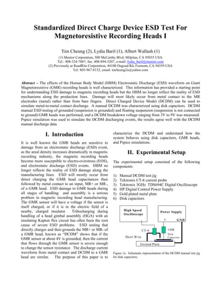
  • 1. Standardized Direct Charge Device ESD Test For Magnetoresistive Recording Heads I Tim Cheung (2), Lydia Baril (1), Albert Wallash (1) (1) Maxtor Corporation, 500 McCarthy Blvd, Milpitas, CA 95035 USA Tel.: 408-324-7067, fax: 408-894-3207, e-mail: lydia_baril@maxtor.com (2) Previously at ReadRite Corporation, 44100 Osgood Rd, Fremont, CA 94359 USA Tel: 805-967-8152, email: tocheung2u@yahoo.com Abstract – The effects of the Human Body Model (HBM) Electrostatic Discharge (ESD) waveform on Giant Magnetoresistive (GMR) recording heads is well characterized. This information has provided a starting point for understanding ESD damage to magnetic recording heads but the HBM no longer reflect the reality of ESD mechanisms along the production lines. Damage will most likely occur from metal contact to the MR electrodes (metal) rather than from bare fingers. Direct Charged Device Model (DCDM) can be used to simulate metal-to-metal contact discharge. A manual DCDM was characterized using disk capacitors. DCDM manual ESD testing of grounded (suspension is grounded) and floating suspension (suspension is not connected to ground) GMR heads was performed, and a DCDM breakdown voltage ranging from 3V to 9V was measured. Pspice simulation was used to simulate the DCDM discharging events, the results agree well with the DCDM manual discharge data. I. Introduction It is well known the GMR heads are sensitive to damage from an electrostatic discharge (ESD) event, as the areal density increases dramatically in magnetic recording industry, the magnetic recording heads become more susceptible to electro-overstress (EOS), and electrostatic discharge (ESD) events. HBM no longer reflects the reality of ESD damage along the manufacturing lines. ESD will mostly occur from direct charging the GMR head capacitances then followed by metal contact to an input, MR+ or MR-, of a GMR head. ESD damage to GMR heads during all stages of handling and assembly is a serious problem in magnetic recording head manufacturing. The GMR sensor will have a voltage if the sensor is itself charged, or if it is in the electric field of a nearby, charged insulator. Tribocharging during handling of a head gimbal assembly (HGA) with an insulating Kapton flex circuit has often been the root cause of severe ESD problems. ESD testing that directly charges and then grounds the MR+ or MR- of a GMR head, known as “DCDM” shows that if the GMR sensor at about 4V is grounded, then the current that flows through the GMR sensor is severe enough to change the sensor resistance. The discharge current waveform from metal contact and DCDM to a GMR head are similar. The purpose of this paper is to characterize the DCDM and understand how the system behaves using disk capacitors, GMR heads, and Pspice simulations. II. Experimental Setup The experimental setup consisted of the following components: 1) Manual DCDM test jig 2) Tektronix CT-6 current probe 3) Tektronix 3GHz TDS694C Digital Oscilloscope 4) HP Digital Control Power Supply 5) Gold plated metal plate 6) Disk capacitors Figure 1a. Schematic representation of the DCDM manual test jig for disk capacitors. High Speed Oscilloscope + GND 10MCT-6 Ground Plate Short Wire Power Supply Disk Capacitor
  • 2. The purpose of using a manual test jig is that it has very small parasitic capacitance and inductance. Figure 1a shows the schematic representation of DCDM manual test jig. The inductanceless disk capacitors are made out of 0.8 mm thick FR-4 double- sided printed circuit board (PCB). One side of the board is gold-plated etched to a circular disk, and the other is gold-plated ground plane. The capacitance depends on the size of a circular disk (the spacing is fixed). The larger the circular disk is the higher the capacitance. Figure 1b shows four different sizes of disk capacitance, 0.5pF, 2.2pF, 4.4pF, and 11.5pF. Figure 1b. Four disk capacitors 0.5pF, 2.2pF, 4.4pF and 11.5pF. Figure 1c. DCDM manual test jig for disk capacitors. The bottom plate of the capacitor lies on a grounded gold-plated metal. The grounded metal plate is gold- plated for good contact between the bottom plate of disk capacitor and metal plate. A voltage source provides voltage to the top plate of the disk capacitor through a 10MΩ resistor. The voltage source is continuously charging the disk capacitor. A short wire of about half inch long is connected to a grounded metal plate through a CT-6 current probe (See Figure 1c). The disk capacitor surface and the grounded wire must be cleaned. The discharge of the disk capacitor is done manually contacting one end of the ground wire to the top disk plate. During discharge process, the manual contact must be very fast and precise. The discharge current waveforms are detected with a CT-6 current probe and the waveforms are captured from a high-speed digital oscilloscope Tektronix TDS 694C 3GHz and 10GS/s. Figure 2 shows that the grounded and floating suspension GMR heads were tested on the same DCDM manual test jig. A grounded suspension HGA means that the suspension contacts the grounded metal plate. A floating suspension HGA means that the suspension is isolated from the grounded metal plate. A 10MΩ resistor is connected from a power supply to the MR+ of a GMR head. Then, the grounded short wire contacts the MR+ or MR- pad for discharge the charged GMR head. The CT-6 current probe captures the discharge current; the high speed oscilloscope is used to monitor the discharge current, and an Ohmmeter is used to measure the MR resistance after each discharge event until the MR resistance changed more than 1%. (Note: Use the MR resistance failure for reference only, magnetic performance is more susceptible to ESD damage). Figure 2. Schematic representation of the DCDM manual test jig for GMR head. III. Experimental Results and Analysis Figure 3 shows a simplified electrical equivalent circuit for DCDM manual test jig. The voltage source is not shown in the circuit. Cdisk is the disk capacitor, L1 is the inductance of the grounded wire, Cp is the parasitic capacitance of the circuit, Rspark is the spark resistance, which is created during the grounded wire contacts the charged disk capacitor. High Speed Oscilloscope + GND 10MCT-6 Metal Plate Short Wire Power Supply HGA 10 MΩ resistor CT6 Short wire Power supply + Ground To Oscilloscope Metal plate
  • 3. Figure 3. Electrical equivalent circuit for DCDM manual testing for disk capacitor. Figure 4 shows an example of discharge current waveform for a disk capacitor 4.4pF at charging voltage of 4V. The first peak current reaches 54mA and the pulse width is about 0.47ns. There is a second peak of opposite polarity or undershoot. Its peak current level is about –21mA. Waveforms obtained in the same manner for the same capacitance and the same charging voltage is mostly reproducible, i.e. peak current and pulse width values are within +/- 10%. Waveforms were captured for a range of capacitor values and charging voltages. Figure 4. Discharge current waveform of a 4.4pF disk capacitor at 4V. Figure 5a shows the manual test discharge current for four different capacitances and voltages. The discharge current equation is given by: )sin()( tetI t L V ωα ω − = (3) where α = R/2L, ω = 2πf = , I(t) is the discharge current and V is the voltage on the capacitor. The equation (3) shows that the voltage on the capacitor is doubled, the discharge current is also doubled. Figure 5b shows that the pulse width decreases as the voltage on the capacitor increases. The hypothesis for the decreasing pulse width at higher voltage are the bandwidth limitation of a CT-6 current probe and the lower spark resistance as a result of smaller change of time constant. Figure 5c shows the discharge current saturated at high capacitance. This is due to the smaller the capacitance, the higher the discharge path impedance, which limits the current. The magnitude of impedance Z is given by: , where ω = 2πf, R is the equivalent resistance of the inductor L1, the L is the inductance of the L1. Pspice simulation will be used to verify this behavior. Manual Charging/Discharging on Disk Capacitors 11.5pF y = 17.786x - 5.5478 4.4pF y = 12.151x - 3.4174 2.2pF y = 5.1043x + 0.0087 0.5pF y = 2.1426x + 0.3652 0 20 40 60 80 100 120 140 160 0 2 4 6 8 10 DCDM Voltage (V) measuredIp(mA) 11.5pF 4.4pF 2.2pF 0.5pF Figure 5a. Charging voltage versus discharge current for four capacitors. Manual DCDM 4.4pF @4V -3.0E-02 -2.0E-02 -1.0E-02 0.0E+00 1.0E-02 2.0E-02 3.0E-02 4.0E-02 5.0E-02 6.0E-02 -1.E-09 0.E+00 1.E-09 2.E-09 3.E-09 4.E-09 5.E-09 Time (ns) PeakCurrent(A) Time (sec.) Cdisk Rspark Cp L1 SW 2 2 1 − ( )L R LC ( )22 LRZ ω+=
  • 4. 0.0 0.2 0.4 0.6 0.8 1.0 1.2 0 2 4 6 8 10 DCDM Voltage (V) PeakWidthatHalfAmplitude(ns) 11.5pF 4.4pF 2.2pF 0.5pF Figure 5b. Pulse width versus charging voltage for four capacitances. 0 20 40 60 80 100 120 140 0 1 2 3 4 5 6 7 8 9 10 11 12 13 Capacitance (pF) Ip(mA) 8V 4V 2V 1V Figure 5c. Discharge current versus capacitance for four charging voltages. Figure 6 shows an electrical circuit model of the DCDM manual testing for grounded suspension GMR heads. The capacitance from the MR leads to suspension is larger than other capacitance when the suspension is grounded. The total capacitance of the HGA depends on the type of flexcircuit. In this particular flexcircuit HGAs, the total capacitance is about 22pF from the MR leads to suspension. Figure 7 shows a simplified equivalent electrical circuit of Figure 6. Where 22pF is the total head capacitance, L1 is the total inductance of the MR lead and inductance of discharge path. Figure 6. Electrical circuit model of the DCDM manual testing for grounded suspension GMR heads. Figure 7. Simplified equivalent electrical circuit model for grounded suspension GMR heads. Figure 8 shows the discharge current of 51mA and the pulse width of about 2ns at 4V for the grounded suspension GMR head. Figure 8. Discharge current waveform at 4V for grounded suspension GMR head. Figure 9 shows the electrical circuit model of the DCDM, and the floating suspension GMR heads (floating suspension means the suspension is not connected to ground). The head capacitance is dominated by the capacitance between the suspension and the system ground. Figure 9. Electrical circuit model of the DCDM and the floating suspension GMR heads. Manual DCDM: Grounded suspension Criteria: MRR > 1% -0.02 -0.01 0 0.01 0.02 0.03 0.04 0.05 0.06 -1.E-09 0.E+00 1.E-09 2.E-09 3.E-09 4.E-09 5.E-09 6.E-09 7.E-09 8.E-09 9.E-09 Time (ns) Totaldischargecurrent(A) breakdown at 4V Time (sec.) Rspark L1 SW CMR-to-grounded suspension 22pF V 30nH30nH10nH 5pF 5pF 11pF 2pF 11pF 0.1pF 5pF DCDM MR 42Ω 1G 2Ω 10G 100G100G Rsp 33Ω 1G MR pad+ MR pad- Bottom Shield System Ground Substrate/Suspension SW V 10MΩ 2Ω 30nH30nH10nH 5pF 5pF 11pF 2pF 11pF 0.1pF 5pF DCDM MR 42Ω 1G 2Ω 10G 100G100G 40 1G MR pad+ MR pad- Bottom Shield System Ground Substrate/Suspension SW 5pF 100G V 10MΩ 2Ω
  • 5. When the GMR head suspension is not grounded, the capacitance from suspension to grounded metal plate is approximately 5pF. Figure 10a shows the CMR-to- suspension in series with the Csuspension-to-ground. The total head capacitance can be calculated as follows: C=(22pF)(5pF)/(22pF+5pF)=4pF Figure 10a. Simplified electrical circuit model for a floating suspension GMR head. Figure 10b shows a simplified head capacitance from MR-to-ground for floating suspension GMR head. An equivalent head capacitance can be represented by a single 4pF. Figure 10b. Simplified electrical circuit model for a floating suspension GMR heads with a total equivalent capacitance of 4pF. Figure 11 shows the discharge current waveforms at different charging voltages from 3V to 9V. The MR resistance of this floating suspension head changed from 42Ω to 54Ω at 9V breakdown. The peak current amplitude at 9V is about 65mA, and the pulse width is about 0.8ns. Figure 11. Discharge current waveform at breakdown voltage of 9V for a floating suspension GMR head. Figure 12 shows that the comparison of the breakdown voltage for the grounded suspension and the floating suspension GMR heads. The grounded suspension heads were broken down at about 3V to 4V, and the floating suspension head was broken down at about 9V at the GMR resistance changing more than 1%. The floating suspension exhibits higher breakdown voltage than the grounded suspension GMR head because the grounded suspension has a larger head capacitance than the floating suspension GMR head reference to grounded metal plate. The grounded suspension HGA has a total head capacitance of about 22pF, and the floating suspension HGA has a total head capacitance of about 4pF. The total head energy to damage to MR sensor can be calculated and compared as follows: For grounded suspension HGA: A total head capacitance C of 22pF with a charging voltage (V) at breakdown of 4V, then the total energy can be calculated based on the equation: E=1/2(C V 2 )=0.176nJ For floating suspension HGA: A total equivalent head capacitance C of 4pF with a charging voltage (V) at breakdown of 9V, then the total energy can be calculated based on the equation: E=1/2(C V 2 )=0.162nJ Comparing the two total energies, the floating suspension HGA requires higher voltage to reach the same energy level as for the grounded suspension HGA that can damage the GMR sensor (assume same MR resistance for both type). This is due to the floating suspension HGA has lower head capacitance than the grounded suspension HGA reference to ground. Csuspension-to-ground CMR-to-suspension Rspark L1 SW 22pF 5pF Rspark L1 SW 4pF V CMR-to-ground M a n u a l DCDM: Floating Suspension -0.04 -0.02 0 0.0 2 0.0 4 0.0 6 0.0 8 -1.00E-09 0.00E+00 1.00E-09 2.00E-09 3.00E-09 4.00E-09 5.00E-09 6 .00E-09 7.00E-09 8.00E-09 9.00E-09 Tim e (ns ) Totaldischargecurrent(A) 3.05V 4V 4.5V 5V 5.5V 6 V 6.5 V 7V 7.5V 8V 8.5V 9 V 2.54V Ip = 65mA @ 9V breakdown PW50 = 0.8ns
  • 6. Figure 12. GMR resistance versus DCDM breakdown voltage for grounded and floating suspension GMR heads. Discharge current occurs when the grounded wire is brought near a charged disk capacitor, the electric field between them increases to an extreme value. When the field exceeds the dielectric breakdown strength of air, current begins to flow by an avalanche process. Eventually a low resistance spark develops. The spark resistance can be affected by the contact conditions such as humidity, contact speed, grounded wire/disk capacitor plate material, the size and the shape of the grounded wire tip and the contamination between the grounded wire tip and the disk capacitor. The following setup can be used for initial spark resistance study. Figure 13 shows the spark resistance test setup. A low inductance surface mount resistor must be used. The purpose of using additional resistance in series with the discharge path is that the behavior of the pulse width and the amplitude of the discharge current can be observed. (See Figure 14) Figure 13. Schematic representation of the spark resistance test setup. Figure 14 shows the discharge current waveforms varying the different series resistances. The higher the series resistance in the discharge path is the lower the discharge current amplitude and wider the pulse width. Both the resistance and impedance of the inductor L1 in the discharge path can affect the discharge current amplitude and the pulse wide. The total resistance, Rt, in the discharge path is approximately related by the following expression: Rt = Rseries + Rspark + | Z | (4) The magnitude of impedance Z is given by: ( )22 LRZ ω+= , (5) where fπω = 2 , R is the equivalent resistance of the inductor wire and L is the equivalent inductance, f is the frequency. The Rspark and the impedance can be calculated from the Equation (4): Rspark + | Z | = Vc/Ip - Rseries where Vc is the charging voltage on the capacitor, and the Ip is the discharging current. Figure 14. Discharge current versus Rseries at charging voltage of 4V. Figure 15 shows the Rspark and the impedance Z as a function of charging voltage. The manual DCDM test jig was used to perform this experiment (See Figure 13). The spark resistance plus the impedance Z without adding the series resistance is 44Ω at 4V. Based on the experimental data, the Rspark plus the impedance Z increase as the charging voltage decreases. However, we expected higher spark resistance with the increasing of the charging voltage. More experiments need to be conducted and analyzed in this area. -0.04 -0.02 0 0.02 0.04 0.06 0.08 0.1 -2.E-09 -1.E-09 0.E+00 1.E-09 2.E-09 3.E-09 4.E-09 5.E-09 6.E-09 7.E-09 8.E-09 Time (sec.) DischargeCurrent(A) No Rseries 11 Ohms 51 Ohms 100 Ohms High Speed Oscilloscope + GND 10MCT-6 Ground Plate Series resistor Power Supply Disk Capacitor Manual DCDM: Grounded vs Floating suspension Criteria: MRR >1% 40 42 44 46 48 50 52 54 56 0 1 2 3 4 5 6 7 8 9 10 DCDM Voltage (V) Col d M RR Hd1 Hd2 Hd3 Hd4 Floating suspensionGrounded suspension
  • 7. Figure 15. Spark resistance versus DCDM voltage IV. Pspice Simulation The DCDM manual discharge behavior can be confirmed by Pspice simulation. Figure 16 shows the Pspice simulation of discharge current waveform from discharging a disk capacitor of 4.4pF at 4V, inductance L1 of 10nH and spark resistance of 24Ω. As can be seen, the DCDM manual discharge waveform and the Pspice simulation waveform are comparable. Figure 16. DCDM manual testing (solid line) and simulation (dashed line) comparison using 4.4pF at 4V. Figure 17. Pspice simulation of discharge current for the grounded suspension GMR head at 4V. Dashed line is the current through GMR sensor. The total current flows through the GMR heads can be measured but the current flows through the GMR sensor can not be measured. Pspice simulation can be used to observe the current flows through the GMR sensor. Figure 17 shows the Pspice simulation of the total discharge current (solid line), and the current flows through the GMR sensor (dashed line) for the grounded suspension GMR head at breakdown voltage of 4V. The discharge current of 22mA flows through the GMR sensor. The reason for the current flows through the GMR sensor less than 50% of the total current because the GMR sensor resistance limits the current. The total discharge current using the manual discharge (See Figure 8), and the Pspice simulation (See Figure 17) for a grounded suspension GMR head are comparable. The Pspice simulated discharge current for the floating suspension GMR head at the breakdown voltage of 9V (See Figure 18) is comparable to the manual discharge (See Figure 11). The total discharge current is about 66mA; 22mA flows through the GMR sensor, and the pulse width is about 0.8ns. Figure 18. Pspice simulation of discharge current for a floating suspension GMR head. Dashed line is the current through GMR sensor. Figure 19 shows the Pspice simulation of discharge current per charging voltage (mA/V) relationship for 4 different disk capacitors. The simulation results agree well with the DCDM manual discharge. Figure 19. Pspice simulation of peak current versus DCDM voltage. 0 20 40 60 80 100 120 140 0 5 10 15 20 DCDM Voltage (V) Rspark+Z(Ohm) Series resistance 51 Ohms Series resistance 11 Ohms Series resistance 100 Ohms Pspice Simulated V vs I vs C y = 16.208x + 0.1125 11.5pF y = 11.13x + 0.5917 4.4pF y = 8.1211x - 0.275 2.2pF y = 2.7734x + 0.125 0.5pF 0 20 40 60 80 100 120 140 160 180 0 2 4 6 8 10 12 DCDM Voltage (V) Ip(mA) -0.03 -0.02 -0.01 0 0.01 0.02 0.03 0.04 0.05 0.06 0.0E+00 1.0E-09 2.0E-09 3.0E-09 4.0E-09 5.0E-09 time (sec.) DischargeCurrent(A) Dashed line: simulated, Ip=54mA, PW50=0.47ns Solid line: manual tested, Ip=54mA, PW50=0.47ns -0.04 -0.02 0 0.02 0.04 0.06 0.08 0.0E+00 1.0E-09 2.0E-09 3.0E-09 4.0E-09 5.0E-09 6.0E-09 7.0E-09 8.0E-09 9.0E-09 time (sec.) DischargeCurrent(A) Solid line: total discharge current = 66mA Dashed line: discharge current through MR = 22mA PW50 = 0.8ns -0.02 -0.01 0 0.01 0.02 0.03 0.04 0.05 0.06 -1.E-09 0.E+00 1.E-09 2.E-09 3.E-09 4.E-09 5.E-09 6.E-09 7.E-09 8.E-09 9.E-09 time (sec.) DischargeCurrent(A) IMR=22mA Itotal=52mA PW50=2ns
  • 8. Figure 20 shows the Pspice simulation of discharge current pulse width as a function of DCDM voltage for 6 different disk capacitors. The spark resistance, inductance and capacitance are no changed. The pulse width maintains constant throughout the charging voltage ranging from 1V to 16V. However, the simulation conditions and the experimental condition is slightly different. The experimental data shows that the spark resistance changes as varying the charging voltage. Figure 20. Pspice simulation of discharge current pulse width versus charging voltage. Figure 21 shows the discharge currents are saturated as increasing the capacitance. The experimental data and simulation data are comparable. 0 20 40 60 80 100 120 140 0 1 2 3 4 5 6 7 8 9 10 11 12 13 Capacitance (pF) PeakCurrent(mA) 4V 8V 2V 1V Figure 21. Pspice simulation of discharge current versus capacitance for four charging voltages. Figure 22 shows that if the DCDM module varies the spark resistance from 10Ω to 60Ω during ESD testing, 75% less energy (not shown) flows through the GMR sensor at 60? . Figure 22. Pspice simulation of discharge current flows through the GMR sensor at the charging voltage of 4V with varying the spark resistance Rsp of the DCDM from 10Ω to 60Ω. Figure 23 shows that if the DCDM module varies the discharge path inductance from 5nH to 65nH, the energy (not shown) increases about 23% at 65nH. Figure 23. Pspice simulation of discharge current flows through the GMR sensor at the charging voltage of 4V with varying the discharge path inductance from 5 to 65nH. V. Data Summary Table 1 shows the rise time of discharge currents for four capacitors at charging voltage ranging from 1V, 2V, 4V and 8V. The experimental (exp) and simulation (sim) results are closed. Table 1. Discharge current risetime comparison for four capacitances at charging voltages ranging from 1V, 2V, 4V and 8V. 0.5pF 2.2pF 4.4pF 11.5pF tr(ns) exp sim exp sim exp sim exp sim V 1 0.25 0.177 0.21 0.203 0.39 0.215 0.53 0.32 2 0.18 0.17 0.25 0.197 0.31 0.226 0.42 0.32 4 0.17 0.175 0.26 0.209 0.29 0.225 0.4 0.32 8 0.14 0.175 0.19 0.192 0.34 0.228 0.44 0.32 Ave 0.19 0.17 0.23 0.20 0.33 0.22 0.45 0.32 -0.02 -0.015 -0.01 -0.005 0 0.005 0.01 0.015 0.02 0.025 0.03 0.035 0.0E+00 2.0E-09 4.0E-09 6.0E-09 8.0E-09 1.0E-08 1.2E-08 1.4E-08 Time (sec.) DischargeCurrentthruMR(A) 10 Ohms 60 Ohms -0.01 -0.005 0 0.005 0.01 0.015 0.02 0.025 0.03 0.0E+0 0 2.0E-09 4.0E-09 6.0E-09 8.0E-09 1.0E-08 1.2E-08 1.4E-08 Time (sec.) DischargeCurrentthruMR(A) 5nH 65nH 0 0.1 0.2 0.3 0.4 0.5 0.6 0.7 0.8 0 2 4 6 8 10 Charging Voltage (V) PW50(ns) 0.5pF 2.2pF 4.4pF 11.5pF
  • 9. Table 2 shows the sensitivity of discharge current per charging voltage (mA/V) for four capacitances. There is about 9% different between experimental and simulation results for both 11.5pF and 4.4pF. Table 2. Discharge current per charging voltage sensitivity comparison for four capacitances. Table 3 shows the pulse width for four capacitances at charging voltage ranging from 1V, 2V, 4V and 8V. The experimental and simulation results are close, but the simulation data are slightly less than the experimental data. Selection of component values for simulation can affect the results. Table 3. Discharge current pulse width comparison for four capacitances at charging voltages ranging from 1V, 2V, 4V and 8V. VI. Conclusion We have learned from the manual testing, and Pspice simulations, the spark resistance; parasitic capacitance and inductance of the DCDM system can change the characteristic of a DCDM discharging current waveform. The Pspice simulation and experimental data are comparable. The data shows the grounded suspension GMR head is more sensitive than the floating suspension GMR head. The spark resistance, the DCDM parasitic inductance and capacitance can affect the results of ESD testing. More spark resistance experiments need to be conducted and analyzed. It is a big challenge for the test equipment vendors to design a DCDM tester with very small parasitic inductance and capacitance. REFERENCES [1] Socket Device Model Testing, ESD Association technical report TR 08-00 [2] The SDM Test Method: Past, Present, and Future. Michael Chaine, Ion Barth, Tilo Bordeck, Leo G. Henry, Mark A. Kelly, and Tom Meusen Compliance Engineering. Ce-mag.com 09-10/2001 [3] Charge Device Model. ESD Association standard test method. ESD STM5.3.1-1999 [4] Standardized Direct Charged Device ESD Test for Magnetoresistive Recording Heads II. Lydia Baril, Tim Cheung, Albert Wallash. Submitted to EOS/ESD Symposium 2002 [5] “Direct Charging” Charge Device Model Testing of Magnetoresistive Recording Heads. Tim Cheung, EOS/ESD Symposium 1997 0.5pF 2.2pF 4.4pF 11.5pF exp sim exp sim exp sim exp sim mA/V 2.14 2.8 5.1 8.1 12.2 11.1 17.8 16.2 0.5pF 2.2pF 4.4pF 11.5pF PW50 exp sim exp sim exp sim exp sim V 1 0.37 0.2 0.44 0.33 0.65 0.46 1.00 0.72 2 0.35 0.2 0.42 0.33 0.58 0.45 0.95 0.72 4 0.34 0.2 0.39 0.33 0.49 0.45 0.85 0.73 8 0.25 0.22 0.43 0.33 0.49 0.46 0.79 0.73 Ave 0.33 0.21 0.42 0.33 0.55 0.46 0.90 0.73