電源回路のデバイスモデリングとLTspiceを活用したノイズシミュレーション
•Als PPTX, PDF herunterladen•
0 gefällt mir•4,246 views

電源回路のデバイスモデリングとLTspiceを活用したノイズシミュレーション

Empfohlen
Weitere ähnliche Inhalte
Was ist angesagt?
Was ist angesagt? (20)
Ähnlich wie 電源回路のデバイスモデリングとLTspiceを活用したノイズシミュレーション
Ähnlich wie 電源回路のデバイスモデリングとLTspiceを活用したノイズシミュレーション (20)
Mehr von Tsuyoshi Horigome
Mehr von Tsuyoshi Horigome (20)
電源回路のデバイスモデリングとLTspiceを活用したノイズシミュレーション
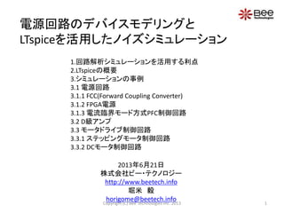
- 1. 電源回路のデバイスモデリングと LTspiceを活用したノイズシミュレーション 2013年6月21日 株式会社ビー・テクノロジー http://www.beetech.info 堀米 毅 horigome@beetech.info 1.回路解析シミュレーションを活用する利点 2.LTspiceの概要 3.シミュレーションの事例 3.1 電源回路 3.1.1 FCC(Forward Coupling Converter) 3.1.2 FPGA電源 3.1.3 電流臨界モード方式PFC制御回路 3.2 D級アンプ 3.3 モータドライブ制御回路 3.3.1 ステッピングモータ制御回路 3.3.2 DCモータ制御回路 1Copyright (C) Bee Technologies Inc. 2013
- 3. ①回路実験では観察しにくい電流波形が簡単に見える コイルの電流波形も1クリック表示 部品の上で電流プローブを表示させてクリックするだけ 1.回路解析シミュレーションを活用する利点 3Copyright (C) Bee Technologies Inc. 2013
- 4. ①回路実験では観察しにくい電流波形が簡単に見える シミュレーション結果より、コイルに8[A]も流れることが判明。コイルには、 直流重畳特性があり、8[A]でもインダクタンス値が変わらないコイルを 選定したい。 1.回路解析シミュレーションを活用する利点 コイルの電流波形も簡単表示 4Copyright (C) Bee Technologies Inc. 2013
- 5. ②損失計算も1クリック ハイサイドのPower MOSFET(Q1)とローサイドのPower MOSFET(Q2)の損失計算 も部品上で「Altキー」を押しながら、クリックで損失波形を簡単表示 1.回路解析シミュレーションを活用する利点 5Copyright (C) Bee Technologies Inc. 2013
- 6. ③ノイズ現象も見れる ハイサイドのPower MOSFET(Q1)のドレイン電流の波形を観察すると、ノイズ現象 が見られる 1.回路解析シミュレーションを活用する利点 6Copyright (C) Bee Technologies Inc. 2013
- 7. 回路解析シミュレーションの活用で、 設計品質を向上させる 安全設計を行う 回路動作を理論的に把握する 回路解析シミュレータは回路設計を効率良く 行うための「道具」です。関数電卓よりは賢い。 1.回路解析シミュレーションを活用する利点 7Copyright (C) Bee Technologies Inc. 2013
- 9. Tr1がONの場合 ON ON 9Copyright (C) Bee Technologies Inc. 2013 3.1.1 FCC(Forward Coupling Converter)
- 10. Tr1がOFFの場合 OFF ON 10Copyright (C) Bee Technologies Inc. 2013 3.1.1 FCC(Forward Coupling Converter)
- 11. 回路モデルの考え方 11Copyright (C) Bee Technologies Inc. 2013 等価的に回路モデルを考える 3.1.1 FCC(Forward Coupling Converter)
- 12. 回路モデルの考え方 トランス2次側入力波形をパルス電源で表現する 整流側ダイオードとフライホイル側ダイオードを忠実に再現する チョークコイルを等価的に考える コンデンサの等価回路を考える 配線長の影響を考慮する 12Copyright (C) Bee Technologies Inc. 2013 3.1.1 FCC(Forward Coupling Converter)
- 13. トランス2次側入力波形 トランス2次側入力波形をパルス電源 に置き換えます。 実際の回路基板があれば、オシロスコープでトランス2次側入力波形を 確認し、その波形をパルス電源に置き換えます。 13Copyright (C) Bee Technologies Inc. 2013 3.1.1 FCC(Forward Coupling Converter) V1:初期電圧 V2:パルス電圧 TD:遅延値 TR:立ち上がり時間 TF:立ち下がり時間 PW:パルス幅 PER:周期値
- 14. 【参考】ダイオードモデルの弱点について ダイオードのパラメータであるTTは、逆回復特性のtrr(trj+trb)のtrjの部分しか 表現出来ません。この弱点を克服する為には、trj+trbを表現する等価回路を作成 する必要があります。 + 等価回路モデル Trjのみ表現可能である 整流側ダイオードとフライホイル側ダイオード 14Copyright (C) Bee Technologies Inc. 2013 3.1.1 FCC(Forward Coupling Converter)
- 15. 整流側ダイオードとフライホイル側ダイオード ここでのポイントは、逆回復特性の表現です。通常のダイオード・モデルパラメータでは正確に逆 回復特性を表現する事が出来ません。ここでは、プロフェッショナル・モデルを採用致します。 Simulation Measurement プロフェッショナルモデルとは、逆回復特性(trj,trb)を忠実に再現した等価回路モデルです。 15Copyright (C) Bee Technologies Inc. 2013 3.1.1 FCC(Forward Coupling Converter)
- 16. チョークコイル チョークコイルは等価的に考えます。本格的にシミュレーションする場合は、 周波数を考慮した等価回路モデルが必要になります。ここでは、特に回路 に影響する要因を考え、等価モデルを作成します。 C4を追加する事で、回路による影響要因を 加える事が出来ます。 16Copyright (C) Bee Technologies Inc. 2013 3.1.1 FCC(Forward Coupling Converter)
- 17. 【参考】インダクタの等価回路の考え方 10 -3 10 0 10 3 10 6 10 9 (Hz) Impedance vs. Frequency Inductor model R1L1 L1 R1 R1L1 C1 L1 10 -3 10 0 10 3 10 6 10 9 (Hz) Impedance vs. Frequency Inductor model R1L1 R1L1 L1 R1 L1 R1 R1L1 C1 R1L1 C1 L1L1 17Copyright (C) Bee Technologies Inc. 2013 3.1.1 FCC(Forward Coupling Converter)
- 18. Frequency 1.0KHz 10KHz 100KHz 1.0MHz 10MHz V(V1:+)/ I(V1) 1.0 10 100 1.0K 10K 100K (2.1878M,234.735K) All Rights Reserved Copyright (C) Bee Technologies Inc. 18Copyright (C) Bee Technologies Inc. 2013 3.1.1 FCC(Forward Coupling Converter)
- 19. ラダー・モデル(Rudder Model) Frequency 100Hz 1.0KHz 10KHz 100KHz 1.0MHz 10MHz 100MHz V(N01685)/I(V2) 10m 100m 1.0 10 100 1.0K 10K 19Copyright (C) Bee Technologies Inc. 2013 3.1.1 FCC(Forward Coupling Converter) C1 1 2 R1 L2 C2 L1 R2 RS *$ *PART NUMBER: SF-T5-25-01-PF *MANUFACTURER: TDK *All Rights Reserved Copyright (c) Bee Technologies Inc. 2006 .SUBCKT SF-T5-25-01-PF 1 2 R1 1 N4 2.89441k RS N4 2 37.9262m C1 1 N4 5.81894p L1 1 N3 12.151u L2 N3 N4 24.0673u R2 N3 N4 592.966 C2 N3 N4 2.2969p .ENDS *$ SPICEシミュレーション結果 インピーダンス測定結果(Agilent 4294A)
- 20. コンデンサ コンデンサの内部にはESRとESLが存在します。回路動作にESR及び ESLが影響する場合は、回路図上に無くても、回路解析シミュレーション をする場合は、具体的な値を入れなくてはいけません。ESR値及びESL値 をサプライヤー企業にお問合わせするか。プレシジョン・インピーダンス・ アナライザで計測を行う必要があります。 20Copyright (C) Bee Technologies Inc. 2013 3.1.1 FCC(Forward Coupling Converter)
- 21. 【参考】 コンデンサの等価回路の考え方 Impedance vs. Frequency Capacitor model 10 -3 10 0 10 3 10 6 10 9 (Hz) Impedance vs. Frequency Capacitor model 10 -3 10 0 10 3 10 6 10 9 (Hz) コンデンサの種類により、ESR値及びESL値には傾向があります。 その特性も考慮しなければなりません。 21Copyright (C) Bee Technologies Inc. 2013 3.1.1 FCC(Forward Coupling Converter) 3素子モデル(3 Elements Model) 電源回路シミュレーションで採用 5素子モデル(5 Elements Model) ラダー・モデル(Rudder Model) CPU周辺及び高速動作の回路シミュレーションで採用
- 22. *$ *PART NUMBER: DE1B3KX101KA5B *MANUFACTURER: MURATA *All Rights Reserved Copyright (c) Bee Technologies Inc. 2013 .SUBCKT DE1B3KX101KA5B 1 4 L1 1 2 39.7352n C1 2 3 92.4504p R1 3 4 2.28354 .ENDS *$ L1 C1 R1 All Rights Reserved Copyright (C) Bee Technologies Inc. 22Copyright (C) Bee Technologies Inc. 2013 3.1.1 FCC(Forward Coupling Converter) SPICEシミュレーション結果 インピーダンス測定結果(Agilent 4294A)
- 23. 電解コンデンサの事例 All Rights Reserved Copyright (C) Bee Technologies Inc. 23Copyright (C) Bee Technologies Inc. 2013 3.1.1 FCC(Forward Coupling Converter) Frequency 100Hz 1.0KHz 10KHz 100KHz 1.0MHz 10MHz 100MHz V(N00027)/ I(V2) 1.0 10 100 1.0K 0 U1 ECEA0JKG470_25C V2 1Vac 0Vdc V1 0Vdc *$ *PART NUMBER: ECEAOJKG470 *MANUFACTURER: Panasonic *All Rights Reserved Copyright (C) Bee Technologies Inc. 2013 .SUBCKT ECEAOJKG470_25C 1 4 L1 1 2 775.427nH C1 2 3 35.762uF R1 3 4 2.04763 .ENDS *$
- 24. 5素子モデル(5 Elements Model) *$ *PART NUMBER: F25case2V1200uF *MANUFACTURER: NIPPON CHEMI-CON *CAP=1200uF,Vmax=2V *All Rights Reserved Copyright (C) Bee Technologies Inc. 2013 .SUBCKT F25case2V1200uF 1 2 C_C2 N1 N3 11uF R_R1 N2 2 942.2070u L_LS 1 N1 1.3500pH C_C1 N1 N2 1.2mF R_R2 N3 2 10u .ENDS *$ 24Copyright (C) Bee Technologies Inc. 2013 3.1.1 FCC(Forward Coupling Converter) 21 R1 LS C1 R2C2 Frequency 100KHz 1.0MHz 10MHz 100MHz 1.0GHz 10GHz V(U1:1)/ I(V1) 10u 100u 1.0m 10m 100m 1.0 SPICEシミュレーション結果 インピーダンス測定結果(Agilent 4294A) V1 1Vac 0Vdc 0 V2 0Vdc U1 F25CASE2V1200UF
- 25. ラダー・モデル(Rudder Model) *$ *PART NUMBER: F25case2V1200uF *MANUFACTURER: NIPPON CHEMI-CON *CAP=1200uF,Vmax=2V *All Rights Reserved Copyright (C) Bee Technologies Inc. 2013 .SUBCKT F25case2V1200uF 1 2 R_R2 N3 N4 14.6480Ω R_R3 N4 N5 11.3548uΩ R_R4 N5 N6 1.998mΩ C_CS 1 N1 1.25mF L_LS N1 N2 1.35pH C_C1 N3 2 11uF C_C2 N4 2 1.9862mF C_C3 N5 2 2.7169mF C_C4 N6 2 2.1047nF R_RS N2 2 905.7567uΩ R_R1 N2 N3 518.3787nΩ .ENDS *$ All Rights Reserved Copyright (C) Bee Technologies Inc. 25Copyright (C) Bee Technologies Inc. 2013 3.1.1 FCC(Forward Coupling Converter) RS R1 R2 R3 R4CS LS C1 C2 C3 C4 1 2Frequency 100KHz 1.0MHz 10MHz 100MHz 1.0GHz 10GHz V(U1:1)/ I(V1) 10u 100u 1.0m 10m 100m 1.0 SPICEシミュレーション結果 インピーダンス測定結果(Agilent 4294A)
- 26. 配線長 配線長の影響が回路動作に与える場合、配線長のインダクタンス値は 回路図にはありませんが、配線長のインダクタンス成分を負荷しなければ なりません。この回路の場合、特に影響度合いが強い箇所に配線長の値 を入れております。L5のインダクタンスは配線長です。 26Copyright (C) Bee Technologies Inc. 2013 3.1.1 FCC(Forward Coupling Converter)
- 27. 収束問題について 回路解析シミュレーションにおいて、収束問題に直面します。回避方法は、 回路図を工夫するか。もしくは.OPTIONで回避するかの2通りがあります。 実際には.OPTIONで回避します。.OPTIONで回避出来ない場合は、 回路図上に問題があると考えた方がいいです。 .OPTION RELTOL=0.01 VNTOL=1m ABSTOL=1n GMIN=1E-10 ITL1=500 ITL2=200 ITL4=40 27Copyright (C) Bee Technologies Inc. 2013 事例 FCC LTspice Version can simulate without .OPTION Settings 3.1.1 FCC(Forward Coupling Converter)
- 28. Simulation Measurement 28Copyright (C) Bee Technologies Inc. 2013 3.1.1 FCC(Forward Coupling Converter)
- 29. Simulation Measurement 29Copyright (C) Bee Technologies Inc. 2013 3.1.1 FCC(Forward Coupling Converter)
- 30. 30Copyright (C) Bee Technologies Inc. 2013 3.1.1 FCC(Forward Coupling Converter)
- 31. Simulation Measurement 31Copyright (C) Bee Technologies Inc. 2013 3.1.1 FCC(Forward Coupling Converter)
- 32. 3.1.2 FPGA電源 32Copyright (C) Bee Technologies Inc. 2013 エミフィル プロードライザー FPGAのコア電圧が1.2[V]の場合、許容電圧範囲は、プラスマイナス50m[V]になります。この許容範囲は非常に小さい値です。 低電圧大電流のため、例えば、10[A]の電流変化が発生した場合、電源ライン(FPGA電源とFPGAの配線間)に5m[Ω]の抵抗成分 があるだけで、許容範囲である50m[V]の電圧変動が発生します。この抵抗成分は、配線の抵抗成分であったり、電源ラインにある デカップリングコンデンサの内部直列抵抗成分(ESR)だったりします。つまり、ESRが5m[Ω]あるだけで、10[A]の電流変化には十分 機能しない電源供給になります。これらを考慮して、ノイズ対策をしなければなりません。
- 33. 3.1.2 FPGA電源 33Copyright (C) Bee Technologies Inc. 2013 B-PSG間の周波数 特性の測定結果 CB-CG間の周波数 特性の測定結果 B-CB間の周波数 特性の測定結果 データシートのデータシート に掲載されていた等価回路図 デバイスモデリングで得られた等価回路図 エミフィルのデバイスモデリング
- 34. 3.1.2 FPGA電源 34Copyright (C) Bee Technologies Inc. 2013 プロードライザーのデバイスモデリング PIN1-GND間の周波数 特性の測定結果 PIN2-GND間の周波数 特性の測定結果 PIN1-PIN2間の周波数 特性の測定結果 デバイスモデリングで得 られた等価回路図
- 35. 3.1.2 FPGA電源 35Copyright (C) Bee Technologies Inc. 2013 出力特性シミュレーション
- 36. 3.1.2 FPGA電源 背景:FPGA電源の出力ラインのノイズを削減する必要性がある。大電流低電圧であり、 許容される電圧変動が小さいため、ノイズ対策が必要である。ノイズ除去フィルター等 を活用する。 LTspice ノイズ除去回路 入力信号 ノイズ波形 出力波形で ノイズの低減 の効果を確認 実際のノイズ波形をオシロスコープで測定し、波形データをCSV形式で取得する 36Copyright (C) Bee Technologies Inc. 2013
- 37. 37Copyright (C) Bee Technologies Inc. 2013 3.1.2 FPGA電源
- 38. 38Copyright (C) Bee Technologies Inc. 2013 3.1.2 FPGA電源
- 39. http://youtu.be/QTy4JOxtZRA 39Copyright (C) Bee Technologies Inc. 2013 3.1.2 FPGA電源
- 40. Most electronic ballasts and switching power supplies use a bridge rectifier and a bulk storage capacitor to derive raw dc voltage from the utility ac line, figure above: Vin=100Vac, 50Hz and PO=200W. Copyright (C) Bee Technologies Inc. 2013 40 Vin AC_IN1 PARAMETERS: f req = 50Hz Vin = 100Vac AC_IN2 Cbulk 2000uF 0 bulkDB1 DB2DB3 Diode DB4 Load 1.414Adc Iline Vbulk 3.1.3 電流臨界モード方式PFC制御回路
- 41. Time 160ms 164ms 168ms 172ms 176ms 180ms 184ms 188ms 192ms 196ms 200ms AVG(ABS(W(Vin)))/(RMS(ABS(V(AC_IN1,AC_IN2)))*RMS(ABS(I(Vin)))) 0 0.2 0.4 0.6 0.8 1.0 ABS( I(Vin) ) 0A 10A 20A ABS( V(AC_IN1,AC_IN2) ) V(bulk) 0V 100V 200V SEL>> The Uncorrected Power Factor rectifying circuit draws current from the ac line when the ac voltage exceeds the capacitor voltage (Vbulk). The current (Iline) is non-sinusoidal. This results in a poor power factor condition where the apparent input power is much higher than the real power, figure above, power factor ratios of 0.5 to 0.7 are common. Copyright (C) Bee Technologies Inc. 2013 41 |VAC, in, 100V| (VPEAK, in=100*2=141.42V) and Vbulk |Iline| Power Factor Ratio = Pin, avg./(Vin, rms* Iin, rms) 3.1.3 電流臨界モード方式PFC制御回路
- 42. Vac, in C1 1uF C2 200u ILoad 0.5A L1 12 Diode D2 Q1 MOSFET R7 L2 1 2 0 0 Rectifiers PFC TB6819AFG Controller Circuit PARAMETERS: f req = 50Hz Vin = 100Vac The Power Factor Correction (PFC) circuit, as an off-line active preconverter, is designed to draw a sinusoidal current from the AC line that is in phase with input voltage. As a result, the power factor ratio is improved to be near to ideal (1). The TB6819AFG is a critical conduction mode (CRM) PFC controller IC. The description including equation and constants as a guide to understand its designing process is included in this document. Copyright (C) Bee Technologies Inc. 2013 42 Iline VDC, OUT 3.1.3 電流臨界モード方式PFC制御回路
- 43. Time*10 100ms 104ms 108ms 112ms 116ms 120ms 124ms 128ms 132ms 136ms 140ms AVG(ABS(W(Vin))) / (RMS(ABS(V(AC_IN1,AC_IN2)))*RMS(ABS(I(Vin)))) 0 0.2 0.4 0.6 0.8 1.0 -I(Vin) -8.0A 0A 8.0A SEL>> 1 V(AC_IN1,AC_IN2) 2 V(VOUT) -160V 0V 160V 1 200V 400V 600V 2 >> The poor power factor load is corrected by keeping the ac line current sinusoidal and in phase with the line voltage. This results with power factor ratio is 0.85. Copyright (C) Bee Technologies Inc. 2013 43 VAC, in, 100V and VDC, OUT, 400V Iline Power Factor Ratio = 0.85 *simulation result at tscale = 10 3.1.3 電流臨界モード方式PFC制御回路
- 44. Load 0.5A R12 39k C9 0.1uF Vin FREQ = {f req} VAMPL = {Vin*1.414} AC_IN1 R4 100 PARAMETERS: f req = 50 Vin = 100 C6 3300p AC_IN2 C1 1u 0 0 R9 3MEG R10 22k C5 10nF C8 47uF IC = 17.9 D5 DZ18V R11 360k R6 68k R8 100k MULT Rtf C3 0.47uF IC = 3.74 L1 {L} 12 PARAMETERS: L = 230u N = {1/9.6} N=N2/N1, L2=(N^2)*L1 VCC V1 R7 0.11 POUT V2 U1 TB6819AFG FB_IN COMP MULT ISZCD GND POUT VCC FB_IN IS ZCD C7 8p R3 10k C4 1uF VOUT R2 1.5MEG R1 9.53k C2 200uF IC = {2.51*1509.53/9.53} COMP L2 {N*N*L} 1 2 K K1 COUPLING = 1 K_Linear L1 = L1 L2 = L2 DB1 Diode D2 Diode D3 Diode D4 DB2DB3 Diode DB4 Q1 MOSFET R5 10 Copyright (C) Bee Technologies Inc. 2013 44 VAC, in=85-265VAC PO = 200W, VDC, OUT = 400VDC *Analysis directives: .TRAN 0 20ms 0 100n .OPTIONS ABSTOL= 100n .OPTIONS GMIN= 1.0E-8 .OPTIONS ITL1= 500 .OPTIONS ITL2= 200 .OPTIONS ITL4= 40 .OPTIONS RELTOL= 0.01 .OPTIONS VNTOL= 100u 3.1.3 電流臨界モード方式PFC制御回路
- 45. Time 18.00ms 18.25ms 18.50ms 18.75ms 19.00ms 19.25ms 19.50ms 19.75ms 20.00ms ID(Q1) -6A 0A 6A 12A V(Q1:d,Q1:s) 0V 200V 400V 600V I(D2) 8A 16A -2A SEL>> V(D2:2,D2:1) 0V 200V 400V 600V Switching Devices VPEAK and IPEAK at Steady State Copyright (C) Bee Technologies Inc. 2013 45 D2 VKA, Peak ≈ 400V at steady state Total simulation time = 976.83 seconds D2 IF, Peak ≈ 12A at steady state Q1 VDS, Peak ≈ 400V at steady state Q1 ID, Peak ≈ 7.2A at steady state 3.1.3 電流臨界モード方式PFC制御回路
- 46. Load 0.5A R12 39k C9 0.1uF Vin FREQ = {f req*tscale} VAMPL = {Vin*1.414} AC_IN1 R4 100 PARAMETERS: f req = 50 Vin = 85 C6 3300p AC_IN2 C1 1u 0 0 R9 3MEG R10 22k C5 {10n/tscale} C8 47uF IC = 17.9 D5 DZ18V R11 360k R6 68k R8 100k MULT Rtf C3 {0.47u/tscale} L1 {L} 12 PARAMETERS: L = 230u N = {1/9.6} N=N2/N1, L2=(N^2)*L1 VCC V1 R7 0.11 POUT V2 U1 TB6819AFG FB_IN COMP MULT ISZCD GND POUT VCC FB_IN ISZCD C7 8p R3 10k C4 {1u/tscale} VOUT R2 1.5MEG R1 9.53k C2 {200u/tscale} PARAMETERS: tscale = 40 COMP L2 {N*N*L} 1 2 K K1 COUPLING = 1 K_Linear L1 = L1 L2 = L2 DB1 Diode D2 Diode D3 Diode D4 DB2DB3 Diode DB4 Q1 MOSFET R5 10 Switching Devices VPEAK and IPEAK at Start Up Copyright (C) Bee Technologies Inc. 2013 46 Vin, min = 85Vac with frequency 50Hz, tscale = 40 Iload = 0.5A as PO=200W at VO=400V I(D2) Switching Diode, D2 *Analysis directives: .TRAN 0 10ms 0m 100n .OPTIONS ABSTOL= 100n .OPTIONS GMIN= 1.0E-8 .OPTIONS ITL1= 500 .OPTIONS ITL2= 200 .OPTIONS ITL4= 40 .OPTIONS RELTOL= 0.01 .OPTIONS VNTOL= 100u ID(Q1) Switching MOSFET, Q1 Rectifier Diode, DB1-4 3.1.3 電流臨界モード方式PFC制御回路
- 47. Time 476us 480us 484us 488us 492us 496us 500us 504us 508us 512us 516us V(V2) 0V 40V -I(L1) 0A 5A 10A V(V1) 0V 250V 500V V(Q1:g) 10V 20V SEL>> Time 0s 0.5ms 1.0ms 1.5ms 2.0ms V(VOUT) 392V 400V Copyright (C) Bee Technologies Inc. 2013 47 The Simulation Waveform with the defaults models V(V1) I (L1) V(V2) V(VOUT) without high frequency ripple which is caused by ESR and ESL of the capacitor model. Gate charge characteristics is not include in the default model. Total simulation time = 132.41 seconds 3.1.3 電流臨界モード方式PFC制御回路
- 48. Load 0.5A R12 39k Q2 2SK2611 C9 0.1uF Vin FREQ = {f req*tscale} VAMPL = {Vin*1.414} AC_IN1 R4 100 PARAMETERS: f req = 50 Vin = 100 C6 3300p AC_IN2 C1 1u 0 0 R9 3MEG R10 22k C5 {10n/tscale} C8 47uF IC = 17.9 D5 DZ18V R11 360k R6 68k R8 100k MULT Rtf C3 {0.47u/tscale} IC = 3.74 L1 {L} 12 PARAMETERS: L = 230u N = {1/9.6} N=N2/N1, L2=(N^2)*L1 VCC V1 R7 0.11 POUT V2 U1 TB6819AFG FB_IN COMP MULT ISZCD GND POUT VCC FB_IN ISZCD C7 8p R3 10k C4 {1u/tscale} VOUT R2 1.5MEG R1 9.53k COMP L2 {N*N*L} 1 2 K K1 COUPLING = 1 K_Linear L1 = L1 L2 = L2 C2 RJJ-35V221MG5-T20 D2 SCS110AG DB1 Diode D3 Diode D4 PARAMETERS: tscale = 10 DB2DB3 Diode DB4 R5 10 Simulation with Models from the SpicePark Copyright (C) Bee Technologies Inc. 2013 48 Capacitor model MOSFET professional model Schottky diode model Replace some default model with models from SpicePark *Analysis directives: .TRAN 0 2ms 0 100n .OPTIONS ABSTOL= 100n .OPTIONS GMIN= 1.0E-8 .OPTIONS ITL1= 500 .OPTIONS ITL2= 200 .OPTIONS ITL4= 100 .OPTIONS RELTOL= 0.01 .OPTIONS VNTOL= 100u 3.1.3 電流臨界モード方式PFC制御回路
- 49. Time 484us 488us 492us 496us 500us 504us 508us 512us 516us 520us 524us V(V2) 0V 40V -I(L1) 0A 5A 10A V(V1) 0V 250V 500V V(Q2:g) 10V 20V SEL>> Time 0s 0.2ms 0.4ms 0.6ms 0.8ms 1.0ms 1.2ms 1.4ms 1.6ms 1.8ms 2.0ms V(VOUT) 392V 400V Simulation with Models from the SpicePark Copyright (C) Bee Technologies Inc. 2013 49 V(VOUT) with high frequency ripple which is caused by ESR and ESL of the capacitor model. Gate charge characteristics is include in the MOSFET Professional model. V(V1) I (L1) V(V2) Total simulation time = 408.13 seconds 3.1.3 電流臨界モード方式PFC制御回路
- 50. Copyright (C) Bee Technologies Inc. 2013 50 パワーMOSFETのスパイスモデルについて MOSFET LEVEL LEVEL=1 Shichman-Hodges Model LEVEL=2 形状に基づいた解析モデル LEVEL=3 半経験則短チャネルモデル LEVEL=4 BSIM Model LEVEL=6 BSIM3 MODEL ・・・・・・・ ・・ MOSFET LEVEL=3 半経験則短チャネルモデルの特徴 (1)2次元的な電位分布によるデバイスの長さ及び幅に対してスレッシュホルド電圧 が敏感に影響を受ける。 (2)ドレインが誘起するBarrier loweringによるドレイン電圧に対してのスレッシュホルド電圧 の考慮。 (3)リニア領域と飽和領域との間での緩やかな変化及びホットエレクトロンの速度 飽和によって若干減少する飽和電圧、飽和電流の考慮。 RB BulkGate Cbs Cgb RG Cgd ROS Cgs RD RS Cbd Drain Source Idrain 3.1.3 電流臨界モード方式PFC制御回路
- 51. Copyright (C) Bee Technologies Inc. 2013 51 Time*1ms 0 8n 16n 24n 32n 40n V(W1:2) V(W201:2) 0V 2V 4V 6V 8V 10V 12V 14V 16V 18V 20V MOSFET LEVEL=3 MODEL Bee Technologies MODEL(Professional) ゲートチャージ特性 ミラー容量が固定値のため、ミラー容量を可変にする 3.1.3 電流臨界モード方式PFC制御回路
- 52. Copyright (C) Bee Technologies Inc. 2013 52 ← 図1 dv/dt Co Io 0 Fig.1 Fig.1の回路図でコンデンサCoにdV/dtなる 立ち上がりを持つ電圧を印加すると流れる 電流は、(1)式になります。 dt dV CoIo ・・・・・・・・・・(1) ここで基準容量Crefを外部電圧VINで制御出来る電圧制御可変容量は、 (2)式になります。 CrefVINVINC )( ・・・・・・・・・・(2) Cref:固定値 3.1.3 電流臨界モード方式PFC制御回路
- 53. Copyright (C) Bee Technologies Inc. 2013 53 I1 1 ABM/I VIN 2 0 図2 Cref 3 I2 1E6*V(2,3)*(V(1,0)-1) ← R1 ← dv/dt C(VIN) Io ← R2 Fig.2 (2)式を満足させる等価回路図(Fig.2)は下記になります。 21 IIIo 21 IIIo ・・・・・・・・・・(3) R2をI2に影響しない微少抵抗(1E-6)とし、IoをC(VIN)に流れる電流と考慮 すると(4)式で表現出来ます。 )3,2(61 2 )3,2( 2 VE R V dt dV CrefI ・・・・・・・・・・(4) 3.1.3 電流臨界モード方式PFC制御回路
- 54. Copyright (C) Bee Technologies Inc. 2013 54 (2),(3),(4)式から dt dV Cref dt dV VINCIIoI )(21 1)0,1()3,2(61 VVE ・・・・・・・・・・(5) dt dV Cref dt dV CrefVIN )3,2(61)1()1( VEVIN dt dV CrefVIN R1はABM/Iなるアナログビヘイビアモデルを使用し、(5)式を満足すれば dt dV CrefVVEIIIo 1)0,1()3,2(6121 ・・・・・・・・・・(6)R1は高抵抗(1E6)とする 3.1.3 電流臨界モード方式PFC制御回路
- 55. Copyright (C) Bee Technologies Inc. 2013 55 C(VIN)は(2)式のように外部電圧VINによって制御出来ます。 C(VIN)>Cref の時、(5)式に従いI1は増加します C(VIN)=Cref の時、I1=0 C(VIN)<Cref の時、 (5)式に従いI1はマイナスになります N13732 N13807 N13744 ABM/I 図3 Run to time: 1us Cref 1u VIN 10v 0 V2 TD = 0 TF = 1us PW = 5us PER = 10us V1 = 0 TR = 1us V2 = 100v Maximum step size: 10ns V1 0Vdc R3 1MEG V(N13732,N13744)*(V(N13807,0)-1)*1E6 R4 1u Fig.3 3.1.3 電流臨界モード方式PFC制御回路
- 56. Copyright (C) Bee Technologies Inc. 2013 56 -Vdg +Vdg Co*(1+Vdg/Vj)^(-M) 図4 0 Co 電圧制御可変容量の等価回路を応用し、ミラー容量に適応させます。 MOSFETのVdg-Cdg特性はFig.4のような特性を示します。 Fig.4 3.1.3 電流臨界モード方式PFC制御回路
- 57. Copyright (C) Bee Technologies Inc. 2013 57 (7)式はVdgが0以下ではCoが一定となります。EVALUEにより、 (7)式によるC(Vdg)を、 M Vj Vdg CoVdgC 1)( ・・・・・・・・・・(7) M Vj Vdg CoVdgE 1)( ・・・・・・・・・・(8) と考え、制御電圧発生回路の出力と考えます。この電圧により、容量可変回 路を制御すればABM/Iの電流はVdgにより、(8)式に従って変化するのでミラー 容量を補正する事が可能になります。 3.1.3 電流臨界モード方式PFC制御回路
- 58. Copyright (C) Bee Technologies Inc. 2013 58 Vdgが0からVdssの区間ではFig.4に示される式にVdg-C(Vdg)特性は依存 し、Vdgがマイナスの区間では容量はCoで一定になります。 G 制御電圧 発生回路 S Vdgリミッタ 図5 EVALUEETABLE → → ABM/I 容量可変回路 Q1 D Fig.5 Fig.5のように制御システムを考慮 すると、Vdgを検出するとETABLE により、Vdgに0~Vdssのリミッタを かけます 3.1.3 電流臨界モード方式PFC制御回路
- 59. 59 Condition : Po = 25[W], 4 Load Analysis Time Domain (Transient) Run to time: 3ms Start saving data after: 1ms Maximum step size: 100n Skip the initial transient bias point calculation (SKIPBP) .Options RELTOL: 0.01 VNTOL: 1.0u ABSTOL: 1.0n CHGTOL: 0.01p GMIN: 1.0E-12 ITL1: 500 ITL2: 200 ITL4: 10 TEST CONDITION: C4 1nF 0 +B 15V + C18 EKMG500ELL222MLP1S C5 1nF 0 R18 10 0 R19 2.2k PARAMETERS: Po = 25W Gv = 15.85 RL = 4 f in = 1kHz C14 MMH250K684 R4 220 C7 10u IC = 10 R2 3k R1 100k C10 22u IC = 15 LOAD {RL} OUT C9 22u IC = 12.85 MUR120RLG D2 IN VS R13 10 R3 47k L1 7G14N-220-RB VB R17 1 R20 3.3k 0 R21 8.2k R8 820 +B VAA 0 VREF R6 8.2k R7 1.2k CSD OCSET IN- IC1 IRS2092 VAA GND IN- COMP CSD VSS VREF OCSET DT COM LO VCC VS HO VB CSH VCC 0 DT VSS 0 COMP R5 820 -B HO R15 10 LO VR1 75 -B -15V 0 C2 10u IC = 7 C8 10u IC = 7 R11 10k V1 FREQ = {f in} VAMPL = {1.4142*SQRT(Po*RL)/Gv } VOFF = 0 VS CSH C13 MMC400K104 0 C12 MMC250K474 R16 10 C11 RPER11H104K2K1A01B C15 RPER11H104K2K1A01B 0 R14 4.7 MUR120RLG D1 0 R9 4.7k + C16 EKMG500ELL222MLP1S C17 RPER11H104K2K1A01B R12 10k C3 RPER11H103K2K1A01B + C1 EKMG500ELL100ME11D C6 AMZ0050J102 FET1 IRFIZ24N FET2 IRFIZ24N Ls1 20nH 1 2 Ls2 20nH 1 2 Ls3 20nH 1 2 Ls4 20nH 1 2 Ls5 20nH 12 Copyright (C) Bee Technologies Inc. 2013 3.2 D級アンプ
- 60. 60 Time 1.0ms 1.5ms 2.0ms 2.5ms 3.0ms 1 AVG(W(LOAD)) -(AVG(W(+B))+AVG(W(-B))) 2 -100*AVG(W(LOAD))/(AVG(W(+B))+AVG(W(-B))) 0W 5W 10W 15W 20W 25W 30W 35W 40W 45W 50W 1 >> 0 10 20 30 40 50 60 70 80 90 100 2 PSUPPLY [W] PO [W] %Efficiency Specifications : Efficiency Simulation Result Copyright (C) Bee Technologies Inc. 2013 3.2 D級アンプ
- 61. + - SPEAKER F120A FET1 IRFIZ24N FET2 IRFIZ24N + C1 EKMG500ELL100ME11D C6 AMZ0050J102C3 RPER11H103K2K1A01B V1 FREQ = {f in} VAMPL = { 1.4142*VOUT/Gv } VOFF = 0 0 C4 1nF +B 15V + C18 EKMG500ELL222MLP1S C5 1nF 0 R18 10 0 R19 2.2k C14 MMH250K684 R4 220 C7 10u IC = 10 R2 3k R1 100k C10 22u IC = 15 OUT C9 22u IC = 12.85 MUR120RLG D2 VS IN R13 10 R3 47k L1 7G14N-220-RB VB R17 1 0 R20 3.3k R21 8.2k R8 820 +B VREF VAA 0 R6 8.2k R7 1.2k CSD OCSET IN- IC1 IRS2092 VAA GND IN- COMP CSD VSS VREF OCSET DT COM LO VCC VS HO VB CSH VCC 0 DT VSS 0 COMP HO R5 820 -B R15 10 LO VR1 75 -B -15V 0 C2 10u IC = 7 C8 10u IC = 7 R11 10k CSH VS C13 MMC400K104 0 C12 MMC250K474 R16 10 C11 RPER11H104K2K1A01B C15 RPER11H104K2K1A01B 0Ls1 20nH 1 2 Ls2 20nH 1 2 Ls3 20nH 1 2 Ls4 20nH 1 2 R14 4.7 MUR120RLG D1 0 R9 4.7k + C16 EKMG500ELL222MLP1S Ls5 20nH 12 C17 RPER11H104K2K1A01B R12 10k PARAMETERS: VOUT = 2 Gv = 15.85 f in = 1k V V V V V V 61 Time 505.0us 510.0us V(VS) -40V 0V 40V Time 505.0us 510.0us V(HO) -40V 0V 40V Time 505us 510us503us 513us V(LO) -20V 0V Time 0.50ms 0.75ms 1.00ms 1.25ms V(IN) 0V -200mV 200mV Time 505.0us 510.0us V(COMP) 0V -1.0V 1.0V Class D amplifier circuit are simulated and compared with measured waveforms from oscilloscope (Tektronix: TDS3054B) Time 0s 0.3ms 0.7ms V(OUT) -4.0V 0V 4.0V Copyright (C) Bee Technologies Inc. 2013 3.2 D級アンプ
- 62. 62 Time 1.988ms 1.990ms 1.992ms 1.994ms 1.996ms 1.998ms V(VS) -40V -30V -20V -10V 0V 10V 20V 30V 40V OUT VS Simulated Measured Copyright (C) Bee Technologies Inc. 2013 3.2 D級アンプ
- 63. 63 Time 1.988ms 1.990ms 1.992ms 1.994ms 1.996ms 1.998ms V(HO) -40V -30V -20V -10V 0V 10V 20V 30V 40V Time 1.992ms 1.994ms 1.996ms 1.998ms 2.000ms 2.002ms V(LO) -40V -30V -20V -10V 0V 10V 20V 30V 40V HO LO Simulated Measured Copyright (C) Bee Technologies Inc. 2013 3.2 D級アンプ
- 64. 64 Self-oscillation frequency = 400kHz (Simulated) Self-oscillation frequency = 400kHz (Measured) Simulated Measured OUT OUT VS VS Self-Oscillating Frequency Copyright (C) Bee Technologies Inc. 2013 3.2 D級アンプ
- 65. + - SPEAKER F120A FET1 IRFIZ24N FET2 IRFIZ24N + C1 EKMG500ELL100ME11D C6 AMZ0050J102C3 RPER11H103K2K1A01B V1 FREQ = 1k VAMPL = 0 VOFF = 0 0 C4 1nF +B 15V + C18 EKMG500ELL222MLP1S C5 1nF 0 R18 10 0 R19 2.2k C14 MMH250K684 R4 220 C7 10u IC = 10 R2 3k R1 100k C10 22u IC = 15 OUT C9 22u IC = 12.85 MUR120RLG D2 VS IN R13 10 R3 47k L1 7G14N-220-RB VB R17 1 0 R21 8.2k R20 3.3k R8 820 +B VREF VAA 0 R6 8.2k R7 1.2k CSD OCSET IN- IC1 IRS2092 VAA GND IN- COMP CSD VSS VREF OCSET DT COM LO VCC VS HO VB CSH VCC 0 DT VSS 0 COMP HO R5 820 -B R15 10 LO VR1 75 -B -15V 0 C2 10u IC = 7 C8 10u IC = 7 R11 10k CSH VS C13 MMC400K104 0 C12 MMC250K474 R16 10 C11 RPER11H104K2K1A01B C15 RPER11H104K2K1A01B 0Ls1 20nH 1 2 Ls2 20nH 1 2 Ls3 20nH 1 2 Ls4 20nH 1 2 R14 4.7 MUR120RLG D1 0 R9 4.7k + C16 EKMG500ELL222MLP1S Ls5 20nH 12 C17 RPER11H104K2K1A01B R12 10k Dead-time 65 Dead-time Mode R20 R21 DT1 (25ns) 3.3k 8.2k DT2 (40ns) 5.6k 4.7k DT3 (65ns) 8.2k 3.3k DT4 (105ns) - < 10k V(DT) Voltage Divider Analysis Time Domain (Transient) Run to time: 1ms Start saving data after: 0.5m Maximum step size: 40n Skip the initial transient bias point calculation (SKIPBP) .Options RELTOL: 0.001 VNTOL: 1.0u ABSTOL: 1.0n CHGTOL: 0.01p GMIN: 1.0E-12 ITL1: 500 ITL2: 200 ITL4: 10 Copyright (C) Bee Technologies Inc. 2013 3.2 D級アンプ
- 66. Dead-time DT1(25ns) 66 Time 0.9976ms 0.9980ms 0.9984ms 0.9988ms 0.9992ms0.9974ms V(LO,-B) V(HO,VS) -4V 0V 4V 8V 12V 16V V(OUT) 0V -400mV 400mV SEL>> DT1(25ns) DT1(25ns) Spike voltage Copyright (C) Bee Technologies Inc. 2013 3.2 D級アンプ
- 67. Dead-time DT3(65ns) 67 Time 0.9976ms 0.9980ms 0.9984ms 0.9988ms 0.9992ms 0.9996ms V(LO,-B) V(HO,VS) -4V 0V 4V 8V 12V 16V V(OUT) 0V -400mV 400mV SEL>> DT3(65ns) DT3(65ns) Spike voltages (Decrease for longer dead time) Copyright (C) Bee Technologies Inc. 2013 3.2 D級アンプ
- 68. + C1 EKMG500ELL100ME11D C6 AMZ0050J102C3 RPER11H103K2K1A01B C17 RPER11H104K2K1A01B + C18 EKMG500ELL222MLP1S FET1 IRFIZ24N FET2 IRFIZ24N + - SPEAKER F120A 0 C4 1nF +B 15V C5 1nF 0 R18 10 0 R19 2.2k C14 MMH250K684 R4 220 C7 10u IC = 10 R2 3k R1 100k C10 22u IC = 15 OUT C9 22u IC = 12.85 MUR120RLG D2 VS IN R13 10 R3 47k L1 7G14N-220-RB VB R17 1 0 R20 3.3k R21 8.2k R8 820 +B VREF VAA 0 R6 8.2k R7 1.2k CSD OCSET IN- IC1 IRS2092 VAA GND IN- COMP CSD VSS VREF OCSET DT COM LO VCC VS HO VB CSH V1 FREQ = 1k VAMPL = 0 VOFF = 0 VCC 0 DT VSS 0 COMP HO R5 820 -B R15 10 LO VR1 75 -B -15V 0 C2 10u IC = 7 C8 10u IC = 7 R11 10k CSH VS C13 MMC400K104 0 C12 MMC250K474 R16 10 C11 RPER11H104K2K1A01B C15 RPER11H104K2K1A01B 0Ls1 20nH 1 2 Ls2 20nH 1 2 Ls3 20nH 1 2 Ls4 20nH 1 2 R14 4.7 MUR120RLG D1 0 R9 4.7k + C16 EKMG500ELL222MLP1S Ls5 20nH 12 R12 10k The total power loss in MOSFET are given by: PTOTAL = PSW+Pcond+Pgd 68 Power losses in the MOSFETs Analysis Time Domain (Transient) Run to time: 500us Start saving data after: 100n Maximum step size: 2n Skip the initial transient bias point calculation (SKIPBP) .Options RELTOL: 0.003 VNTOL: 1.0m ABSTOL: 100n CHGTOL: 0.01p GMIN: 1.0E-12 ITL1: 500 ITL2: 200 ITL4: 20 Copyright (C) Bee Technologies Inc. 2013 3.2 D級アンプ
- 69. Time 23.6us 24.4us 25.2us 26.0us 26.8us 27.6us 1 V(FET1:S,FET1:D) 2 -I(Ls1) 3 V(FET1:D,FET1:S)*-I(Ls1) 0V 100V -60V 1 -1.5A -1.0A -0.5A 0A 0.5A 1.0A 1.5A 2.0A 2.5A 2 >> -50W 0W 20W 3 Power losses FET1(Professional Model) 69 FET1: ID and VDS are simulated and compared with scope (Tektronix: TDS3054B) waveforms PSW ,Pcond ,and Pgd are calculated by PSpice. VDS, ID (Measured) -VDS ID -VDS ID Power loss (VDS*ID) PSWPgd Pcond VDS, ID (Simulated) Copyright (C) Bee Technologies Inc. 2013 3.2 D級アンプ
- 70. Time 492.8us 493.6us 494.4us 495.2us 496.0us 1 V(FET2:D,FET2:S) 2 -I(Ls3:1) 3 V(FET2:D,FET2:S)*-I(Ls3:1) 0V 100V -40V 1 -1.0A -0.5A 0A 0.5A 1.0A 1.5A 2.0A 2.5A 3.0A 2 >> -50W 0W 20W 3 Power losses FET2(Professional Model) 70 FET2: ID and VDS are simulated and compared with scope (Tektronix: TDS3054B) waveforms PSW ,Pcond ,and Pgd are calculated by PSpice. VDS ID VDS ID Power loss (VDS*ID) PSWPgd Pcond VDS, ID (Measured)VDS, ID (Simulated) Copyright (C) Bee Technologies Inc. 2013 3.2 D級アンプ
- 71. • Gate charge characteristics in Professional model has more accurate results than standard model. FET: IRFIZ24N Qg Standard vs. Professional Model 71 IRFIZ24N (Standard) IRFIZ24N (Professional) VDD=44V,ID=10A ,VGS=10V Measurement Simulation Error (%) Standard Model: Qg(nc) 13.400 12.543 -6.396 Professional Model: Qg(nc) 13.400 13.409 0.067 Copyright (C) Bee Technologies Inc. 2013 3.2 D級アンプ
- 72. Time 867us 869us 871us 873us 875us 877us 1 V(OUT) 2 V(VS) -1.0V -0.5V 0V 0.5V 1.0V 1.5V 2.0V 2.5V 3.0V 1 >> -120V -80V -40V 0V 40V 2 72 Simulated (without output capacitor models) Measured OUT OUT VS VS Self-oscillation frequency = 400kHz (Simulated) Self-oscillation frequency = 400kHz (Measured) Simulation Result (without Capacitor Model) Copyright (C) Bee Technologies Inc. 2013 3.2 D級アンプ
- 73. 73 Simulated (with output capacitor models) Measured OUT OUT VS VS Self-oscillation frequency = 400kHz (Simulated) Self-oscillation frequency = 400kHz (Measured) Simulation Result (with Capacitor Model) Copyright (C) Bee Technologies Inc. 2013 3.2 D級アンプ
- 74. Application Circuit Copyright (C) Bee Technologies Inc. 2013 74 O_A O_A1 O_B1 O_B O_B RRSA 0.5ohm O_B1 V5 Vref AB 1.25Vdc O_A1 O_A RSB L2 IC = 0 1 2 0 Cv ref AB 1uF 00 L1 IC = 0 12 RSA RRSB 0.5ohm 0 VM1 24V CVM1 100uF 00 U1 TB62206FG CCP1 = 0.22UF CCP2 = 0.01UF VM = 24 COSC = 560PF ROSC = 3.6K FIN CR VDD VREF_A VREF_B RS_B RS_A VM CCP_C CCP_B CCP_A STANDBY OUT_A1 PHASE_A PHASE_B OUT_A OUT_B ENABLE_A ENABLE_B OUT_B1 TORQUE V_PHASE_A TD = 0 TF = {tf phase} PW = {pwphase} PER = {tphase} V1 = 0 TR = {trphase} V2 = 5V V_PHASE_B TD = {tphase/4} TF = {tf phase} PW = {pwphase} PER = {tphase} V1 = 0V TR = {trphase} V2 = 5 0 0 PARAMETERS: f phase = 250Hz tphase = {1/f phase} tdphase = {trphase+pwphase/2} pwphase = {-2*trphase+tphase/2} trphase = 100n tf phase = {trphase} VDD 5Vdc C1 10uF 0 0 Rosc 3.6kohm 0 Cosc 560pF 0 Cccp_1 0.22uF Cccp_2 0.022uF 250Hz Full Step Ph_B Ph_A Ph_B Ph_A 3.3.1 ステッピングモータ制御回路
- 75. O_B1 O_B O_A O_A1 RSB 7.9ohm L2 9.15mH IC = -0.5 1 2 L1 9.15mH IC = -0.5 12 RSA 7.9ohm O_A O_A1 O_B1 O_B RRSA 0.5ohm V5 Vref AB 1.25Vdc 0 Cv ref AB 1uF 00 RRSB 0.5ohm 0 VM1 24V CVM1 100uF 00 U1 TB62206FG CCP1 = 0.22UF CCP2 = 0.01UF VM = 24 COSC = 560PF ROSC = 3.6K FIN CR VDD VREF_A VREF_B RS_B RS_A VM CCP_C CCP_B CCP_A STANDBY OUT_A1 PHASE_A PHASE_B OUT_A OUT_B ENABLE_A ENABLE_B OUT_B1 TORQUE V_PHASE_A TD = {tphase/4} TF = {tf phase} PW = {pwphase} PER = {tphase} V1 = 0 TR = {trphase} V2 = 5V V_PHASE_B TD = {tphase/2} TF = {tf phase} PW = {pwphase} PER = {tphase} V1 = 0V TR = {trphase} V2 = 5 0 0 PARAMETERS: f phase = 250Hz tphase = {1/f phase} tdphase = {trphase+pwphase/2} pwphase = {-2*trphase+tphase/2} trphase = 100n tf phase = {trphase} VDD 5Vdc C1 10uF 0 0 Rosc 3.6kohm Cosc 560pF 0 0 Cccp_1 0.22uF Cccp_2 0.022uF 250Hz Full Step Ph_B Ph_A Ph_B Ph_A 3.1 Full Step Switching Sequence Copyright (C) Bee Technologies Inc. 2013 75 Full-step sequences control signals Analysis Time Domain (Transient) Run to time: 8ms Start saving data after: 0ms Maximum step size: - .Options RELTOL: 0.01 VNTOL: 1.0m ABSTOL: 1.0n CHGTOL: 1p GMIN: 1.0E-12 ITL1: 500 ITL2: 200 ITL4: 100
- 76. Full Step Switching Sequence Copyright (C) Bee Technologies Inc. 2013 76 • This figure shows the simulation result of the circuit with Full- step switching sequence. Phase A Phase B Enable A Enable B IOUT A IOUT B Time 0s 4.0ms 8.0ms I(U1:OUT_B1) -1.0A 0A 1.0A I(U1:OUT_A1) -1.0A 0A 1.0A V(U1:ENABLE_B) 0V SEL>> V(U1:ENABLE_A) 0V V(PH_B) 0V V(PH_A) 0V 3.3.1 ステッピングモータ制御回路
- 77. Time 2.54ms 2.58ms I(U1:OUT_B1) 400mA 600mA I(U1:OUT_A1) 400mA 600mA SEL>> Output Ripple Current • This figure shows the output ripple current of the Mixed Decay Mode ,which consist of Charge ,Slow decay ,and Fast decay mode ,with 101kHz chopping frequency. Copyright (C) Bee Technologies Inc. 2013 77 IOUT = 0.5A fchop = 101kHz IOUT A IOUT B Charge mode Slow decay mode Fast decay mode 3.3.1 ステッピングモータ制御回路
- 78. Time 2.593ms 2.595ms 2.597ms 2.599ms 2.601ms 2.603ms I(U1:OUT_A1) 300mA 400mA 500mA 600mA 700mA SEL>> Ripple Current Simulation • The simulation result shows the current ripple that agrees to the measurement data. Copyright (C) Bee Technologies Inc. 2013 78 Current ripple Current ripple Simulation Measurement 3.3.1 ステッピングモータ制御回路
- 79. Parameter Settings If there is no measurement data, the default value will be used: Rm: motor winding resistance [] Lm: motor winding inductance [H] Data is given by D.C. motor spec-sheet: V_norm: normal voltage [V] mNm: normal load [mNm] kRPM_norm: speed at normal load [kr/min] I_norm: current at normal load [A] Load Condition: IL: load current [A] Copyright (C) Bee Technologies Inc. 2013 79 Model Parameters: D.C. Motor model and Parameters with Default Value - + U1 SMPL_DC_MOTOR Rm = 0.1 Lm = 100u I_norm = 6.1 mNm = 19.6 V_norm = 7.2 kRPM_norm = 14.4 IL = 6.1 3.3.2 DCモータ制御回路
- 80. Copyright (C) Bee Technologies Inc. 2013 80 Time 0s 40ms 80ms 120ms 160ms 200ms 240ms 280ms 320ms 360ms 400ms I(VIM) 0A 10A 20A V(VM) 0V 5V 10V SEL>> I(X_U1.V_kRPM) 0A 10A 20A V(X_U1.TRQ) 0V 40V 80V D.C. Motor Current = 6.1A D.C. Motor Voltage = 7.2V D.C. Motor Speed = 14.4krpm Torque Load= 19.6mNm 3.3.2 DCモータ制御回路
- 81. Time 0s 40ms 80ms 120ms 160ms 200ms 240ms 280ms 320ms 360ms 400ms I(VIM) 0A 10A 20A V(VM) 0V 5V 10V I(X_U1.V_kRPM) 0A 10A 20A SEL>> V(X_U1.TRQ) 0V 40V 80V Copyright (C) Bee Technologies Inc. 2013 81 D.C. Motor Current = 3.05A D.C. Motor Voltage = 8.725V D.C. Motor Speed = 18.4krpm Torque Load= 9.8mNm 3.3.2 DCモータ制御回路
- 82. - + U2 SMPL_DC_MOTOR Rm = 0.576 Lm = 165u I_norm = 2.9 mNm = 9.8 V_norm = 7.2 kRPM_norm = 14.2 IL = 0.6 NC NC NCA K VCC VO GND U1 TLP350 V1 TD = 0 TF = 10n PW = 199.99u PER = 400u V1 = 0 TR = 10n V2 = 1.8 0 R1 1u 0 Vcc 15V 0 VCC VDD 0 RG 120 0 DGT10J321_s D3 VCC Vdd 15V VDD 0 D4001 D2 U3 GT10J321 Copyright (C) Bee Technologies Inc. 2013 82 Simplified D.C. Motor with RS- 380PH Spec at No load. Simulation Circuit and Setting No load IL=0.6 Application Example 3.3.2 DCモータ制御回路
- 83. Time -100ms 0s 100ms 300ms 500ms 700ms 900ms 1 I(U2:1) 2 V(U2:1,U2:2) -2A 0A 2A 4A 6A 8A 10A 12A 14A 1 -60V -50V -40V -30V -20V -10V 0V 10V 20V 2 >> Application Example Copyright (C) Bee Technologies Inc. 2013 83 Measurement Simulation Motor Current (2A/Div) Motor Voltage (10V/Div) 3.3.2 DCモータ制御回路
- 84. Time 898.0ms 898.4ms 898.8ms 899.2ms 899.6ms 1 I(U3:C) 2 V(U3:C) 3 V(U3:G) -2A 0A 2A 4A 6A 8A 10A 12A 14A 1 >> -30V -20V -10V 0V 10V 20V 30V 40V 50V 2 -60V -50V -40V -30V -20V -10V 0V 10V 20V 3 Application Example Copyright (C) Bee Technologies Inc. 2013 84 Measurement Simulation IGBT: VGE IGBT: VCE IGBT: IC IGBT: VGE (10V/Div) IGBT: VCE (10V/Div) IGBT: IC (2A/Div) 3.3.2 DCモータ制御回路
- 85. Copyright (C) Bee Technologies Inc. 2013 85 質疑・応答