Design of a Fully Differential Folded-Cascode Operational Amplifier
1. Winter 2008 Designers: Steven Ernst and Jon Provancher Page 1
I. INTRODUCTION
This project entailed the design of a fully differential
operational amplifier with the design specifications and
resultant performance listed in table I. To meet these
requirements, a folded-cascode configuration was chosen
using a triple cascaded nmos and pmos with a second
common source stage. Additionally, there will be one ideal
current source tied to ground for bias and two ideal voltage
sources for VDD and VCM. HSPICE simulations were performed
using 0.25 μm CMOS models with ad=as=W*(0.66 μm) and
pd=ps=2*W+1.32 μm. The simulation was completed for
three scenarios; typical (temp=27
o
C), slow (temp=100
o
C), and
fast (-40
o
C). +20% component values and VDD = 2.375 V were
used for slow case and -20% and VDD = 2.625 V for fast case.
II. BIASING THE AMPLIFIER
Before proceeding with the design to achieve the
specifications in table I, the biasing of the transistors must be
done. We chose a channel length of 0.42 μm corresponding
to layout size requirements. Then we biased all necessary
transistors into the saturation region at all three temperature
settings, taking into account VDS > VGS - VT.
III. DESIGN
At higher temperatures, the bandwidth requirements will
become the most difficult to achieve. Conversely, at lower
temperatures the phase margin will be the parameter of
concern. With this in mind, we began our design by looking
into the higher temperature condition first.
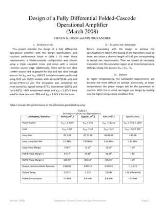
Table I includes the performance of the schematic generated op-amp.
TABLE I
SCHEMATIC GENERATED PERFORMANCE
Constraints / Variables Slow (100
o
C) Typical (27
o
C) Fast (-40
o
C) Specifications
Power Supply VDD = 2.375V VDD = 2.5V VDD = 2.625V VDD = 2.5േ 0.125V
Load Cload = 6pF Cload = 5pF Cload = 4pF Cload = 5pFേ 1pF
Loop Gain 83.3 dB 81.37 dB 80.86 dB > 80 dB
Loop Unity-Gain BW 5.3 MHz 7.69 MHz 9.16 MHz > 50 MHz
Loop Phase Margin 73.87
o
73.24
o
72.57
o
> 70
o
CMFB Phase Margin 1 67.17
o
65.98
o
62.64
o
> 45
o
CMFB Phase Margin 2 106.94
o
106.63
o
105.26
o
> 45
o
Output Common Mode Accuracy 0.0025V 0.0011V 0.0002V < േ 0.1V
Output Swing 2.001V 2.11V 2.034V > 2V differential
Power Consumption 7.9 mW 8.4 mW 8.9 mW < 10 mW
Design of a Fully Differential Folded-Cascode
Operational Amplifier
(March 2008)
STEVEN G. ERNST and JON PROVANCHER
2. Winter 2008 Designers: Steven Ernst and Jon Provancher Page 2
FIGURE I
COMPREHENSIVE SCHEMATIC
3. Winter 2008 Designers: Steven Ernst and Jon Provancher Page 3
IV. DESIGN MODIFICATION
For this design, four separate net-lists were maintained in order to expedite the testing process. The first was used to ensure
transistor saturation, power consumption, and output common mode accuracy. Once this was verified, the other net-lists were used
to test loop parameters, common mode feedback phase margin, and output swing given changes to transistor sizing and bias points.
The first net-list was a simple operating point test done using all components of the amplifier. The second net-list, to determine
loop parameters, performed an AC analysis of the amplifier broken between the input and output. The third net-list, to determine
common mode feedback phase margin, performed an AC analysis of the amplifier broken at the common mode feedback input. The
final net-list performed a DC sweep of the inputs and measured the response at the output. Given this process, it took
approximately five iterations to achieve reasonable results.
V. LAYOUT
In order to ensure project completion, we started the layout
given a design that did not meet all specifications. By planning
out the configuration ahead of time, we were able to create a
neat, concise, and fairly efficient layout. DRC error checks were
performed frequently throughout the layout process to prevent
future problems. Once the preliminary layout was completed,
an LVS check was performed and all of these errors were also
fixed. Finally, once the schematic and layout matched, a net-list
could be generated from the layout. Figure II and figure III
shows the final layout configuration.
TABLE II
LAYOUT EXTRACTED PERFORMANCE
Constraints / Variables Typical (27
o
C) Specifications
Power Supply VDD = 2.5V VDD = 2.5േ 0.125V
Load Cload = 5pF Cload = 5pFേ 1pF
Loop Gain 85.89 dB > 80 dB
Loop Unity-Gain BW 8.36 MHz > 50 MHz
Loop Phase Margin 70.364
o
> 70
o
CMFB Phase Margin 1 54.896
o
> 45
o
CMFB Phase Margin 2 108.5
o
> 45
o
Output Common Mode Error 0.0053V < േ 0.1V
Output Swing 1.35V > 2V differential
Power Consumption 8.2 mW < 10 mW
FOM = (8.36/50)*(70.36/70)*(85.89/80)*(1.35/2)*(10/8.2) = 0.15
VI. CONCLUSION
As shown in table I, the design of a fully differential folded-cascode operational amplifier shown in figure I adheres to the majority of
the specifications. In addition, the performance from the layout, shown in table II, can be noted to be similar to the schematic.
FIGURE II
LAYOUT CONFIGURATION
4. Winter 2008 Designers: Steven Ernst and Jon Provancher Page 4
FIGURE II
LAYOUT CONFIGURATION (AREA OF INTEREST)
5. Winter 2008 Designers: Steven Ernst and Jon Provancher Page 5
VII. APPENDICES
SCHEMATIC EXTRACTED RESULTS
Loop Gain, Loop Bandwidth, and Loop Phase Margin for slow (100o
C)
Loop Gain, Loop Bandwidth, and Loop Phase Margin for typical (27o
C)
Loop Gain, Loop Bandwidth, and Loop Phase Margin for fast (-40o
C)
6. Winter 2008 Designers: Steven Ernst and Jon Provancher Page 6
Output Swing Determination Method
Output Swing and Output Common Mode Error for slow (100o
C)
7. Winter 2008 Designers: Steven Ernst and Jon Provancher Page 7
Output Swing and Output Common Mode Error for typical (27o
C)
Output Swing and Output Common Mode Error for fast (-40o
C)
8. Winter 2008 Designers: Steven Ernst and Jon Provancher Page 8
Common Mode Feedback Phase Margin for slow (100o
C)
Our circuit utilizes two independent common mode feedbacks (one per stage). For this reason, we displayed the phase
margin from each stage.
9. Winter 2008 Designers: Steven Ernst and Jon Provancher Page 9
Common Mode Feedback Phase Margin for typical (27o
C)
10. Winter 2008 Designers: Steven Ernst and Jon Provancher Page 10
Common Mode Feedback Phase Margin for fast (-40o
C)
11. Winter 2008 Designers: Steven Ernst and Jon Provancher Page 11
VIII. INTRODUCTION
A Butterworth Biquad (second-order filter) with 22kHz corner frequency was developed using the designed operational amplifier.
The goal of the design is to obtain a flat response at low frequencies, and a -40 dB/dec drop after the corner frequency.
IX. DESIGN
There are three filter response types known as Butterworth,
Chebyshev, and Bessel. The Biquad filter has the unique
characteristic of producing two polarities of lowpass output.
The Butterworth filter has a flatter response in the passband
than the other topologies.
Using the specified design formulas, obtained from Texas
Instruments, a Butterworth Biquad can be developed. A fully
differential configuration of such can be seen in Figure I. The
results of the designed butterworth biquad is shown in table I.
TABLE I
BUTTERWORTH BIQUAD PERFORMANCE
Evaluated Scenarios Corner Frequency
Slow (temp=100
o
C) 21.89 kHz
Typical (temp=27
o
C) 26.54 kHz
Fast (-40
o
C) 30.86 kHz
FORMULAS
TEXAS INSTRUMENTS BUTTERWORTH DESIGN
• C = C1 = C2
• R = R3 = R2 / 0.707
• Fo = 1 / (2*ߨ*R*C)
• Gain = -R2 / R1
FIGURE I
FULLY DIFFERENTIAL BUTTERWORTH BIQUAD TOPOLOGY
Butterworth Biquad
(March 2008)
STEVEN G. ERNST
12. Winter 2008 Designers: Steven Ernst and Jon Provancher Page 12
X. APPENDICES
SIMULATION RESULTS
Butterworth Biquad Corner Frequency for slow (100o
C)
Butterworth Biquad Corner Frequency for typical (27o
C)
Butterworth Biquad Corner Frequency for fast (-40o
C)