Analysis of harmonics and resonances in hvdc mmc link connected to AC grid
Adjoint Network Analysis of a CMOS Differential Pair
1. 1 of 9
Abstract— The adjoint network analysis can be used to
efficiently determine the sensitivity of a system response from
component parameter variations. This paper performs an adjoint
network on a five transistor CMOS differential pair, and
continues by performing a sensitivity analysis on each of the five
components.
I. INTRODUCTION
he sensitivity model approach is a convenient method of
calculation the effect of specific sensitivities on the
response of the overall system. To do so, one must first
solve a network with a node admittance matrix which is the
transpose of the original circuit. The analysis of a network
which corresponds to the transposed matrix will provide the
sensitivities. This network is known as the adjoint network.
II. ADJOINT NETWORK DESIGN PROCESS
An adjoint network can be formed from the original circuit. To
transform from the original network the the adjoint network,
one must apply the following three rules.
1. Linear resistors are not modified. They are reciprocal
elements which make symmetric contributions to the node
admittance matrix.
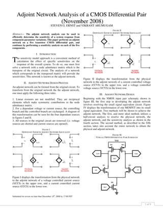
2. For a dependant voltage or current source, the controlling
branch and the controlled branch are exchanged. A diagram of
this transformation can be seen for the four dependant sources
in figures I and II.
3. All sources in the original circuit are removed (i.e. voltage
sources are shorted and current sources are opened).
FIGURE I
DEPENDANT SOURCES ADJOINT NETWORK EQUIVALENT
Figure I displays the transformation from the physical network
to the adjoint network of a voltage controlled current source
(VCCS) in the upper row, and a current controlled current
source (CCCS) in the lower row.
Submitted for review no later than December 14th
, 2008 by 17:00 PST
FIGURE II
DEPENDANT SOURCES ADJOINT NETWORK EQUIVALENT
Figure II displays the transformation from the physical
network to the adjoint network of a current controlled voltage
source (CCVS) in the upper row, and a voltage controlled
voltage source (VCVS) in the lower row.
III. ADJOINT NETWORK DESIGN
Beginning with the NMOS input pair schematic shown in
figure III, the first step in developing the adjoint network
involves resolving the small signal equivalent circuit. Figure
IV displays the transformation of one MOSFET into its small
signal equivalent. Two methods will be shown to achieve the
adjoint network. The first, and more ideal method, utilizes a
half-circuit analysis to resolve the physical network, the
adjoint network, and the sensitivity analysis as shown in the
fourth section. The second method, as described in the fifth
section, takes into account the entire network to obtain the
physical and adjoint network.
FIGURE III
TYPICAL CMOS DIFFERENTIAL PAIR SCHEMATIC
Adjoint Network Analysis of a CMOS Differential Pair
(November 2008)
STEVEN G. ERNST and VIKRANT ARUMUGAM
T
2. 2 of 9
Figure II is simply the collection of five small signal
equivalent MOSFETs arranged in a specific order to form a
CMOS differential pair.
FIGURE IV
SMALL SIGNAL EQUIVALENT OF A SINGLE MOSFET
Figure IV demonstrates how to transform a typical MOSFET
into its small signal equivalent. With this transformation and
the schematic of a CMOS differential pair, we can develop the
physical network of the CMOS differential pair.
IV. HALF-CIRCUIT APPROACH
The first approach taken, the ideal approach (due to
simplicity), is to develop the adjoint network from the half-
circuit analysis. From there, we can move on to section VI
where the sensitivities are calculated by the adjoint network of
the half-circuit for a CMOS differential pair. Figure V
displays the physical network obtained from summation of
information from figure III and figure IV, however, the half-
circuit approach incorporations only a portion of the circuit
shown in figure III. Figure VI displays the relevant half-circuit
equivalent that should be utilized.
FIGURE V
PHYSICAL NETWORK OF THE CMOS DIFFERENTIAL PAIR
Gm2Vgs2
Gm4Vsg4
Gm1Vgs1
Gm3Vsg3
Gm5Vgs5
1 / gds4
1 / gds2
1 / gds3
1 / gds1
1 / gds5
Vin = Vgs2
Vip = Vgs1
Vsg3 = Vsg4
Full size versions of figures V, VII, VIII, and IX are shown in
the appendix.
FIGURE VI
HALF-CIRCUIT OF A CMOS DIFFERENTIAL PAIR
The following steps require designing the physical network
from figure V to account for the modifications due to the half-
circuit equivalent. The new physical network is shown in
figure VII.
FIGURE VII
HALF-CIRCUIT EQUIVALENT OF THE PHYSICAL NETWORK
Full size versions of figures V, VII, VIII, and IX are shown in
the appendix. The same physical network is redrawn for
convenience. It can be seen that Vsg3 = 0, so the resultant
network is reduced. Keep in mind that full size versions of
figures V, VII, VIII, and IX are shown in the appendix.
FIGURE VIII
REDUCED HALF-CIRCUIT EQUIVALENT OF THE PHYSICAL NETWORK
Taking into consideration the three rules listen in the Adjoint
Network Design Process, figure IX is the resolved adjoint
network for the CMOS differential pair. This adjoint network
is developed due to the half-circuit approach. Equally so, this
is the same adjoint network used in the calculation of the
sensitivities.
FIGURE IX
HALF-CIRCUIT ADJOINT NETWORK OF THE CMOS DIFFERENTIAL PAIR
3. 3 of 9
V. FULL-CIRCUIT APPROACH
The second approach taken, an alternative approach is to
develop the adjoint network from the full circuit analysis.
While this approach could be used, this approach will not be
taken to identify the sensitivities as we believe the half-circuit
approach provides a more simplistic approach towards solving
the sensitivities calculated by the adjoint network of the
CMOS differential pair. Figure X displays the physical
network obtained from summation of information from figure
III and figure IV.
FIGURE X
PHYSICAL NETWORK OF THE CMOS DIFFERENTIAL PAIR
Gm2Vgs2
Gm4Vgs4
Gm1Vgs1
Gm3Vgs3
Gm5Vgs5
1 / gds4
1 / gds2
1 / gds3
1 / gds1
1 / gds5
Vin = Vgs2Vip = Vgs1
Vgs3 = Vgs4
Full size versions of figures X, XI, and XII are shown in the
appendix. Taking into consideration the three rules listen in
the Adjoint Network Design Process, figure IX is the resolved
adjoint network for the CMOS differential pair.
FIGURE XI
ADJOINT NETWORK OF THE CMOS DIFFERENTIAL PAIR
Full size versions of figures X, XI, and XII are shown in the
appendix. With nothing but reorganizing the previous adjoint
network, the reduced schematic in figure X is resolved.
FIGURE XII
REDUCED ADJOINT NETWORK OF THE CMOS DIFFERENTIAL PAIR
VI. SENSITIVITY ANALYSIS
A sensitivity analysis is a study to determine how much an
output (either voltage or current) will vary based on variations
within the schematic. As the gds resistance and gm will vary
within the CMOS differential pair, the output will vary as
well. Therefore, a sensitivity analysis will be done to identify
the maximum amount of variation that can occur from an all
varying components.
Below are the abstract formulas used to identify each
element’s specific sensitivity. These formulas were taken from
the half-circuit analysis in section four. A summation of the
individual component’s sensitivity multiplied by its maximum
variation yields the maximum variation to be expected at the
output. The maximum variation of the output voltage can be
found from equation 11. Please note that the calculations done
to identify these equations are shown in the appendix.
|
∆
ೞభ
| ൌ
డ
డೞభ
ൌ
భ
ିଶሺೞభାೞయሻమ ܸ (eq. 1)
|
∆
ೞమ
| ൌ
డ
డೞమ
ൌ
మ
ିଶሺೞమାೞరሻమ ܸ (eq. 2)
|
∆
ೞయ
| ൌ
డ
డೞయ
ൌ
య
ିଶሺೞభାೞయሻమ ܸ (eq. 3)
|
∆
ೞర
| ൌ
డ
డೞర
ൌ
ర
ିଶሺೞమାೞరሻమ ܸ (eq. 4)
ቚ
∆
ೞఱ
ቚ ൌ
డ
డೞఱ
ൌ 0 (eq. 5)
|
∆
భ
| ൌ
డ
డ௩భ
ൌ
ଵ
ሺೞభାೞయሻ
ܸ (eq. 6)
|
∆
మ
| ൌ
డ
డ௩మ
ൌ
ଵ
ሺೞమାೞరሻ
ܸ (eq. 7)
|
∆
య
| ൌ
డ
డ௩య
ൌ 0 (eq. 8)
|
∆
ర
| ൌ
డ
డ௩ర
ൌ 0 (eq. 9)
|
∆
ఱ
| ൌ
డ
డ௩ఱ
ൌ 0 (eq. 10)
|∆ܸெ| ൌ ቚ
డ
డೞభ
∆݃ௗ௦ଵெቚ ቚ
డ
డೞమ
∆݃ௗ௦ଶெቚ
ቚ
డ
డೞయ
∆݃ௗ௦ଷெቚ ቚ
డ
డೞర
∆݃ௗ௦ସெቚ |
డ
డೞఱ
∆݃ௗ௦ହெ|
|
డ
డ௩భ
∆݃ଵெ| |
డ
డ௩మ
∆݃ଶெ| |
డ
డ௩య
∆݃ଷெ|
|
డ
డ௩ర
∆݃ସெ| |
డ
డ௩ఱ
∆݃ହெ| (eq. 11)
As an example of what variation is to be expected, we have
taken typical values for gm, 5 ߤA/V, and gds,
ଵ
ହஐ
, to
demonstrate the sensitivity of a CMOS differential pair with a
1%, 5% and 10% variation of each element. Table I
demonstrates the differential variation. The input voltage is
taken to be 1V.
TABLE IA
DIFFERENTIAL VARIATION
1% Variation 5% Variation 10% Variation
߲ܸ
߲݃ௗ௦ଵ
15.625 15.625 15.625
߲ܸ
߲݃ௗ௦ଶ
15.625 15.625 15.625
߲ܸ
߲݃ௗ௦ଷ
15.625 15.625 15.625
߲ܸ
߲݃ௗ௦ସ
15.625 15.625 15.625
4. 4 of 9
TABLE IB
DIFFERENTIAL VARIATION
1% Variation 5% Variation 10% Variation
߲ܸ
߲ݒଵ
2500 2500 2500
߲ܸ
߲ݒଶ
2500 2500 2500
Table II demonstrates the variation in each element.
TABLE II
ELEMENT VARIATION
1% Variation 5% Variation 10% Variation
∆݃ௗ௦ଵெ 0.02µ 0.1µ 0.2µ
∆݃ௗ௦ଶெ 0.02µ 0.1µ 0.2µ
∆݃ௗ௦ଷெ 0.02µ 0.1µ 0.2µ
∆݃ௗ௦ସெ 0.02µ 0.1µ 0.2µ
∆݃ௗ௦ହெ 0.02µ 0.1µ 0.2µ
∆݃ଵெ 0.05µ 0.25µ 0.5µ
∆݃ଶெ 0.05µ 0.25µ 0.5µ
∆݃ଷெ 0.05µ 0.25µ 0.5µ
∆݃ସெ 0.05µ 0.25µ 0.5µ
∆݃ହெ 0.05µ 0.25µ 0.5µ
Equation 12 shows the calculations for the maximum change
in the output voltage with a 1% variance in components.
|∆ܸெ| ൌ |ሺ15.625ሻሺ0.02µሻ| |ሺ15.625ሻሺ0.02µሻ|
|ሺ15.625ሻሺ0.02µሻ| |ሺ15.625ሻሺ0.02µሻ| |ሺ0ሻሺ0.02µሻ|
|ሺ2500ሻሺ0.05µሻ| |ሺ2500ሻሺ0.05µሻ| |ሺ0ሻሺ0.05µሻ|
|ሺ0ሻሺ0.05µሻ| |ሺ0ሻሺ0.05µሻ| (eq. 12)
Equation 13 shows the calculations for the maximum change
in the output voltage with a 5% variance in components.
|∆ܸெ| ൌ |ሺ15.625ሻሺ0.1µሻ| |ሺ15.625ሻሺ0.1µሻ|
|ሺ15.625ሻሺ0.1µሻ| |ሺ15.625ሻሺ0.1µሻ| |ሺ0ሻሺ0.1µሻ|
|ሺ2500ሻሺ0.25µሻ| |ሺ2500ሻሺ0.25µሻ| |ሺ0ሻሺ0.25µሻ|
|ሺ0ሻሺ0.25µሻ| |ሺ0ሻሺ0.25µሻ| (eq. 13)
Equation 14 shows the calculations for the maximum change
in the output voltage with a 10% variance in components.
|∆ܸெ| ൌ |ሺ15.625ሻሺ0.2µሻ| |ሺ15.625ሻሺ0.2µሻ|
|ሺ15.625ሻሺ0.2µሻ| |ሺ15.625ሻሺ0.2µሻ| |ሺ0ሻሺ0.2µሻ|
|ሺ2500ሻሺ0.5µሻ| |ሺ2500ሻሺ0.5µሻ| |ሺ0ሻሺ0.5µሻ|
|ሺ0ሻሺ0.5µሻ| |ሺ0ሻሺ0.5µሻ| (eq. 14)
With the example of gm, 5 ߤA/V, and gds,
ଵ
ହஐ
, we can
conclude the output voltage variance is as shown below in
table III. To do these calculations, a program was written in
MATLAB. The code used to obtain these calculations can be
found in the appendix.
TABLE III
OUTPUT VOLTAGE VARIATION
1% Variation 5% Variation 10% Variation
|∆ܸெ| 0.375 mV 1.875 mV 3.75 mV
VII. ACKNOWLEDGMENTS
In addition to the listed references, information used
throughout the paper was taken from general knowledge
obtained by the authors throughout their educational career,
industrial career, and hobbyist projects.
VIII. REFERENCES
[1] Wikipedia. “Sensitivity analysis.” November 1, 2008.
http://en.wikipedia.org/wiki/Sensitivity_analysis
[2] Gabor Temes. Professor. School of Electrical Engineering
and Computer Science. Oregon State University.
[3] Gabor Temes. “Lecture notes for ECE 580.” Fall 2008.
Oregon State University
5. 5 of 9
IX. APPENDIX
A. CALCULATIONS TO IDENTIFY |
∆
ೞ
|
ADJOINT NETWORK: Formulas taken from the half-circuit equivalent of the adjoint network shown in figure IX…
1. ݆ଷ
′
ൌ ݆ଵ
′
െ 1
2. ݆ଵ
′
ൌ
ೞయ
ೞభାೞయ
3. ݆ଷ
′
ൌ ሺെ݃ௗ௦య
ሻ
ᇲ
ଶ
4. ݆ଵ
′
ൌ ݃ௗ௦భ
ᇲ
ଶ
5. ܸଵ
ᇱ
ൌ ܸଷ
ᇱ
ൌ ܸ
ᇱ
and ܸହ
ᇱ
ൌ 0
݆ଷ
′
ൌ
ݎௗ௦భ
ݎௗ௦భ
ݎௗ௦య
െ 1 ൌ
െݎௗ௦భ
ݎௗ௦భ
ݎௗ௦య
݆ଷ
′
ൌ ݆ଵ
′
െ 1 and ݆ଷ
′
ൌ ሺെ݃ௗ௦య
ሻ
ᇲ
ଶ
and ݆ଵ
′
ൌ ݃ௗ௦భ
ᇲ
ଶ
so… ܸ
ᇱ
ൌ ܸଵ
ᇱ
ൌ ܸଷ
ᇱ
ൌ
ଶ
ሺೞభାೞయሻ
Due to the half-circuit analysis, we know… ܸଵ
ᇱ
ൌ ܸଶ
ᇱ
ൌ ܸ
ᇱ
and ݆ଶ
′
ൌ
ೞర
ೞమାೞర
and ݆ସ
′
ൌ
ିೞమ
ೞమାೞర
and ܸଶ
ᇱ
ൌ ܸସ
ᇱ
ൌ
ଶ
ሺೞమାೞరሻ
PHYSICAL NETWORK: Formulas taken from the half-circuit equivalent of the physical network shown in figure VIII…
1. െ
బ
ଶ
ൌ െݎௗ௦య
݆ଷ
2. െ
బ
ଶ
ൌ െݎௗ௦భ
݆ଵ
3. ݆ଶ ݆ଵ ൌ ݆ଷ
4. ݆ଶ ൌ ݃ଵ
ಿ
ଶ
5. ܸ௦భ
ൌ
ಿ
ଶ
and ܸ௦య
ൌ ܸ௦ఱ
ൌ 0
െ
బ
ଶ
ൌ െݎௗ௦య
݆ଷ and െ
బ
ଶ
ൌ െݎௗ௦భ
݆ଵ so… ݆ଵ ൌ െ
ೞయ
ೞభ
݆ଷ
݆ଶ ݆ଵ ൌ ݆ଷ and ݆ଶ ൌ ݃ଵ
ಿ
ଶ
so… ݃ଵ
ಿ
ଶ
െ
ೞయ
ೞభ
݆ଷ ൌ ݆ଷ
݆ଷ ൌ
݃ଵ
൬1
ݎௗ௦య
ݎௗ௦భ
൰
ܸூே
2
ൌ
ݎௗ௦భ
݃ଷ
൫ݎௗ௦భ
ݎௗ௦య
൯
ܸூே
2
݆ଵ ൌ െ
ݎௗ௦య
ݎௗ௦భ
݆ଷ ൌ
െݎௗ௦య
ݎௗ௦భ
ݔ
ݎௗ௦భభ
ݎௗ௦భ
ݎௗ௦య
ܸூே
2
ൌ
െݎௗ௦య
݃ଵ
൫ݎௗ௦భ
ݎௗ௦య
൯
ܸூே
2
Due to the half-circuit analysis, we know… ܸ௦మ
ൌ
ಿ
ଶ
and ܸ௦ర
ൌ 0
and ݆ସ ൌ
ೞమర
൫ೞమାೞర൯
ಿ
ଶ
and ݆ଶ ൌ
ೞరమ
൫ೞమାೞర൯
ಿ
ଶ
7. 7 of 9
B. MATLAB CODE
%% Calculation of Sensitivities
clear all;
format short eng;
% Assuming practical values for gm and gds of CMOS transistors
Vin = 1 ; % units in Volts
gm1 = 5e-6 ; gm2 = 5e-6 ; gm3 = 5e-6 ; gm4 = 5e-6 ; gm5 = 5e-6 ; % units in A/V
gds1 = 1/5000 ; gds2 = 1/5000 ; gds3 = 1/5000 ; gds4 = 1/5000 ; gds5 = 1/5000; % units in mhos
% Assuming Variation of 1%,5% and 10% from above said nominal values
var1 = .01; % 1% Variation
var5 = .05; % 5% Variation
var10 = .10; % 10% Variation
Sgds1 = abs((-gm1/(2*(gds1+gds3)^2))*Vin)
Sgds2 = abs((-gm2/(2*(gds2+gds4)^2))*Vin)
Sgds3 = abs((-gm3/(2*(gds1+gds3)^2))*Vin)
Sgds4 = abs((-gm4/(2*(gds2+gds4)^2))*Vin)
Sgds5 = 0 ;
Sgm1 = abs((1/(gds2+gds4))*Vin)
Sgm2 = abs((1/(gds1+gds3))*Vin)
Sgm3 = 0 ;
Sgm4 = 0 ;
Sgm5 = 0 ;
% Sensitivity Analysis on the Output Voltage of the CMOS diff pair
dVo_1percent = Sgds1*gds1*var1 + Sgds2*gds2*var1 + Sgds3*gds3*var1 + Sgds4*gds4*var1 +Sgds5*gds5*var1 +
Sgm1*gm1*var1 + Sgm2*gm2*var1 + Sgm3*gm3*var1 + Sgm4*gm4*var1 + Sgm5*gm5*var1
dVo_5percent = Sgds1*gds1*var5 + Sgds2*gds2*var5 + Sgds3*gds3*var5 + Sgds4*gds4*var5 +Sgds5*gds5*var5 +
Sgm1*gm1*var5 + Sgm2*gm2*var5 + Sgm3*gm3*var5 + Sgm4*gm4*var5 + Sgm5*gm5*var5
dVo_10percent = Sgds1*gds1*var10 + Sgds2*gds2*var10 + Sgds3*gds3*var10 + Sgds4*gds4*var10 +Sgds5*gds5*var10 +
Sgm1*gm1*var10 + Sgm2*gm2*var10 + Sgm3*gm3*var10 + Sgm4*gm4*var10 + Sgm5*gm5*var10
8. 8 of 9
C. FULL SIZE SCHEMATICS
FIGURE V(FULL SIZE)
PHYSICAL NETWORK OF THE CMOS DIFFERENTIAL PAIR
FIGURE VII(FULL SIZE)
HALF-CIRCUIT EQUIVALENT OF THE PHYSICAL NETWORK
FIGURE VIII(FULL SIZE)
REDUCED HALF-CIRCUIT EQUIVALENT OF THE PHYSICAL NETWORK
FIGURE IX(FULL SIZE)
HALF-CIRCUIT ADJOINT NETWORK OF THE CMOS DIFFERENTIAL PAIR
9. 9 of 9
FIGURE X(FULL SIZE)
PHYSICAL NETWORK OF THE CMOS DIFFERENTIAL PAIR
FIGURE XI (FULL SIZE)
ADJOINT NETWORK OF THE FULL-CIRCUIT CMOS DIFFERENTIAL PAIR
FIGURE XII (FULL SIZE)
REDUCED ADJOINT NETWORK OF THE FULL-CIRCUIT CMOS DIFFERENTIAL PAIR