This document discusses different types of transistors. It begins by defining what a transistor is and who invented it. It then describes the basic components of a bipolar junction transistor (BJT) including the emitter, base, and collector. It explains that BJTs can be NPNP or PNP type depending on layer orientation. The document discusses operating regions for transistors based on biasing of the emitter and collector junctions. It also covers different transistor configurations including common base, common emitter, and common collector. Input and output characteristics are described for the common base and common emitter configurations. Current gain is defined and equations are provided.
Call Girls In Bangalore ☎ 7737669865 🥵 Book Your One night Stand
unit 2 part1 (1).pptx
1. Transistors
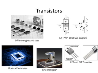
Different types and sizes
BJT (PNP) Electrical Diagram
First Transistor
Modern Electronics
FET and BJT Transistor
2. TRANSISTOR
•Transistor is a device which transfers applied
signal from one type of resister to other type, for
example signal can be transferred from low
resistor to high or from high resistor to low
resistor. By combination of two words transfer
and resister it is called “Transistor” (Transfer
+resistor).
•John Bardeen, Walter Brattain & William
Schokley invented Transistor in 1947
4. BJT (Bipolar Junction Transistor)
•The BJT has three portions inside it, namely the
emitter, the base and the collector, denoted by E,
B and C respectively.
•Emitter: Emitter is a portion of transistor through
which charge carriers enter into it.
•Base: Base is a portion of transistor which
controls the flow of charge carriers between
emitter and collector.
•Collector: Collector is a portion of transistor at
which charge carriers are collected.
5. BJT (Bipolar Junction Transistor)
• BJT can be classified into two types:
1. npn transistor
2. pnp transistor
In n-p-n type a thin layer of p-type is sandwiched
between two layers of n-type semiconductor.
6. BJT (Bipolar Junction Transistor)
•
•In p-n-p type, a thin layer of n-type is
sandwiched between two layers of p type
semiconductor.
7. BJT (Bipolar Junction Transistor)
•In BJT, the emitter layer is heavily doped, the
base lightly doped, and the collector only lightly
doped.
•The outer layers have widths much greater than
the sandwiched p- or n-type material.
•Area and doping profile of these regions are
given as:
Area profile: C>E>B
Doping profile: E>C>B
8. Operation of Transistor
• Operation of transistor is dependent on the
biasing of emitter and collection junction.
• As we know there are two junction in the BJT and
each junction can biased in two ways either
forward bias or reverse bias.
• It means operation of BJT can be dependent on
following four situations:
9. Operation of Transistor
• Emitter junction is forward based and collector
junction is reversed bias. In this situation BJT will be
called in active region and BJT will be used as an
amplifier.
• Emitter junction is forward base and collector
junction is also forward bias. In this situation BJT will
be called in saturation region and it will be used as a
switch.
10. Operation of Transistor
• Emitter junction is reverse bias and collector junction
is also reversed bias in this situation BJT will be called
in Cut off Region and it will be used as switch.
• Emitter junction is reversed bias and collector
junction is forward bias. In this situation BJT will be
called reversed active and there is no use of this type
of biasing.
11. Operation of Transistor in Active
Region
• To operate BJT in active region JEB (emitter base
junction) must be forward biased and JCB (collector
base junction) must be reverse biased.
12. Operation of Transistor in Active
Region
• JEB is forward biased by the battery VEE by which the
depletion region will decrease and a majority carrier
flow will occur from emitter to base giving current
Imajority or IE.
• So, Here, IeE is current due to electrons of emitter
region and IhB is current due to holes in base region.
13. Operation of Transistor in Active
Region
• In base region there is recombination between
electrons and holes due to which base current is
obtained. As number of holes in base is very small,
base current is very small.
• JCB is reverse biased by VCC. So collector current is due
to flow of minority charge carriers from both sides of
the junction. In base minority carriers are electrons
left after recombination and in collector minority
carriers are holes. So,
• Directions of all terminal currents are shown in figure
and it is clear that,
14. Operation of Transistor in Active
Region
• Directions of all terminal currents are shown in figure
and it is clear that,
15. Transistor Configurations
• We know that, transistor can be used as an
amplifier. For an amplifier, two terminals are
required to supply the weak signal and two
terminals to collect the amplified signal.
• Thus four terminals are required but a transistor
is said to have only three terminals Therefore,
one terminal is used common for both input
and output.
16. Transistor Configurations
This gives rise to three different combinations.
• Common base configuration (CB)
• Common emitter configuration (CE)
• Common collector configuration (CC)
19. Input V/I Characteristics of CB Configuration
• It is graph between input current (IE) and input
voltage (VEB) at constant output voltage (VCB).
This graph is drawn for active region of BJT.
20. Input V/I Characteristics of CB Configuration
• By keeping constant VCB, when forward bias at emitter base junction is
increased then graph between IB and VEB is similar to forward
characteristics of pn junction diode. If this graph is again drawn for some
higher value of VCB a similar graph is obtained with reduced knee voltage.
21. Output V/I Characteristics of CB Configuration
• It is graph between output current IC and
output voltage VCE at constant input current IE.
This graph is drawn for all three operating
regions of BJT.
• To draw the graph in active region equation of
output current,
22. Output V/I Characteristics of CB Configuration
• For given and IE, IC is dependent only on I0 which is slightly
dependent on VCB. So, graph of active region is almost
independent of VCB.
• When the transistor is switched from active to saturation
region, a large change in collector current for very small
forward bias voltage at collector to base junction is obtained
in negative direction.
• When both the junctions are reverse biased, a very small
collector current is obtained which is close to horizontal axis.
23. Current Gain of CB Configuration
•In active region equation of
output current can be give as,
Here I0 is reverse saturation current in CB configuration also
written as ICBO
So,
ICBO can be neglected as compared to IC and IE
Then,
Here, α is called dc current of CB Configuration and its value
is around 0.99
25. Input V/I Characteristics of CE Configuration
•It is graph between input current (IB) and input voltage
(VBE) at constant output voltage (VCE). This graph is drawn
for active region of BJT.
•By keeping constant VCE, when forward bias at emitter
base junction is increased then graph between IE and VBE
is similar to forward characteristics of pn junction diode.
26. Input V/I Characteristics of CE Configuration
If this graph is again drawn for some higher value of VCE a similar
graph is obtained with increased knee voltage. This is due to
reduction in IB on increasing reverse bias at collector base
junction.
28. Output V/I Characteristics of CE Configuration
•It is graph between output current IC and
output voltage VCE at constant input current IB.
This graph is drawn for all three operating
regions of BJT.
•To draw the graph in active region equation of
output current,
29. Output V/I Characteristics of CE Configuration
For given and IB, IC is dependent on ( +1)I0
which is more dependent on VCE than in case of
CB configuration. So, graph of active region
has some slope showing change in IC on
changing VCE
32. Current Gain in CE Configuration
• Expression of output current Ic can be given as,
Ic
= α IE + ICBO
= α (IC + IB )+ ICBO
IC (1- α)= α IB + ICBO
Let,
then,
So, Ic
= βIB + (β +1)ICBO
33. Current Gain in CE Configuration
• β is called dc current gain of CE configuration.
• The second term of equation, Ic
= βIB + (β +1)ICBO
is reverse saturation current in CE configuration
and represented as ICEO.
So, ICEO
= (β +1)ICBO