Analog Electronics TIMER IC 555
•Als PPTX, PDF herunterladen•
0 gefällt mir•177 views

timer ic 555

Empfohlen
Weitere ähnliche Inhalte
Was ist angesagt?
Was ist angesagt? (20)
Ähnlich wie Analog Electronics TIMER IC 555
Ähnlich wie Analog Electronics TIMER IC 555 (20)
Kürzlich hochgeladen
Kürzlich hochgeladen (20)
Analog Electronics TIMER IC 555
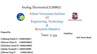
- 1. Arham Veerayatan Institute Of Engineering, Technology & Research.(Mandvi) Prepared by.. (1)Matang Prabaht D (150920109001) (2)Sonara Chetan R (150920109003) (3)Chauhan Anand M (160923109004) (4)Jadeja Yaxrajsinh I (160923109008) (5)Parmar Deep D (160923109013) Guided by:- Prof. Pravin Barad. Analog Electronics(2130902) Timer ic-555
- 2. 555 Timer 2 This presentation will • Introduce the 555 Timer. • Derive the characteristic equations for the charging and discharging of a capacitor. • Present the equations for period, frequency, and duty cycle for a 555 Timer Oscillator. Going Further…. • Detail the operation of a 555 Timer Oscillator. • Derive the equations for period, frequency, and duty cycle for a 555 Timer Oscillator.
- 3. What is a 555 Timer? • The 555 timer is an 8-pin IC that is capable of producing accurate time delays and/or oscillators. • In the time delay mode, the delay is controlled by one external resistor and capacitor. • In the oscillator mode, the frequency of oscillation and duty cycle are both controlled with two external resistors and one capacitor. • This presentation will discuss how to use a 555 timer in the oscillator mode. 3
- 4. Capacitor • A capacitor is an electrical component that can temporarily store a charge (voltage). • The rate that the capacitor charges/discharges is a function of the capacitor’s value and its resistance. • To understand how the capacitor is used in the 555 Timer oscillator circuit, you must understand the basic charge and discharge cycles of the capacitor. 4
- 5. Capacitor Charge Cycle 5 Initial RC-t/ InitialFinalC Ve-1VVV Equation for Charging Capacitor chargetobeginsitascapacitortheacrossvoltageinitialAnyV chargedfullyisthatcapacitortheacrossvoltageTheV capacitortheacrossvoltageTheV :Where Initial Final C • Capacitor is initially discharged. • Switch is moved to position A. • Capacitor will charge to +12 v. • Capacitor will charge through the 2 K resistor.
- 6. Capacitor Discharge Cycle 6 -t/RC FinalInitialC eVVV Equation for Discharging Capacitor dischargetobeginsitascapacitortheacrossvoltageinitialAnyV dischargedfullyisthatcapacitortheacrossvoltageTheV capacitortheacrossvoltageTheV :Where Initial Final C • Capacitor is initially charged. • Switch is moved to position B. • Capacitor will discharge to +0 v. • Capacitor will discharge through the 3 K resistor.
- 7. Capacitor Charge & Discharge 7 0 v 12 v Switch has been at position B for a long period of time. The capacitor is completely discharged. Switch is moved to position A. The capacitor charges through the 2K resistor. Switch is moved back to position B. The capacitor discharges through the 3K resistors. 20 mSec 5 V VC Time
- 8. Block Diagram for a 555 Timer Control Voltage (5) Threshold Voltage (6) Trigger Voltage (2) Ground (1) Vcc (8) Discharge (7) Reset (4) Output (3) - + - + RESET SET Q Q COMP1 COMP2 Flip-Flop T1 8
- 9. Schematic of a 555 Timer in Oscillator Mode 5 Volts N/C N/C Discharge Threshold / Trigger Ground Output1.666 V 3.333 V RA RB C 9
- 10. 555 Timer Design Equations 10 tHIGH : Calculations for the Oscillator’s HIGH Time CRR0.693 BA HIGH t 5v 3.333 v Vc 1.666 v 0 v tHIGH Output HIGH LOW THE OUTPUT IS HIGH WHILE THE CAPACITOR IS CHARGING THROUGH RA + RB.
- 11. 555 Timer Design Equations 11 C0.693RB LOW t tLOW : Calculations for the Oscillator’s LOW Time 5v 3.333 v Vc 1.666 v 0 v tLOW Output HIGH LOW THE OUTPUT IS LOW WHILE THE CAPACITOR IS DISCHARGING THROUGH RB.
- 12. 555 Timer – Period / Frequency / DC 12 CR2R693.0T CR693.0CRR693.0T ttT CR693.0t CRR693.0t BA BBA LOWHIGH BLOW BAHIGH Period: CR2R693.0 1 F T 1 F BA Frequency: %100 R2R RR DC %100 CR2R693.0 CRR693.0 DC %100 T t DC BA BA BA BA HIGH Duty Cycle:
- 13. Example: 555 Oscillator 13 Example: For the 555 Timer oscillator shown below, calculate the circuit’s, period (T), frequency (F), and duty cycle (DC).
- 14. Example: 555 Oscillator 14 Solution: F6.8C180R390R BA mSec534.3T F8.61802390693.0T CR2R693.0T BA Hz282.941F mSec534.3 1 F T 1 F %76DC %100 1802390 180390 DC %100 R2R RR DC BA BA Period: Frequency: Duty Cycle:
- 15. Example: 555 Oscillator 15 Example: For the 555 Timer oscillator shown below, calculate the value for RA & RB so that the oscillator has a frequency of 2.5 KHz @ 60% duty cycle.
- 16. Example: 555 Oscillator 16 Solution: BA BA BABA BABA BA BA BA BA R5.0R R2.0R4.0 R2.1R6.0RR R2R6.0RR 6.0 R2R RR %60%100 R2R RR DC Frequency: Duty Cycle: 09.1228R2R 09.1228 f47.0693.0 Sec400 R2R Sec400f47.0R2R693.0T Sec400CR2R693.0T Sec400 kHz5.2 1 f 1 T BA BA BA BA Two Equations & Two Unknowns!
- 17. Example: 555 Oscillator 17 Solution: BA R5.0R Frequency: Duty Cycle: 09.1228R2R BA Substitute and Solve for RB 23.491R 09.1228R5.2 09.1228R2R5.0 09.1228R2R B B BB BA 618.245R 09.1228472.982R 09.1228491.232R 09.1228R2R A A A BA Substitute and Solve for RA
- 18. 18 Going Further… 555 Oscillator Detail Analysis
- 19. Detail Analysis of a 555 Oscillator 19 5v 3.333 v Vc 1.666 v 0 v RESET HIGH LOW SET HIGH LOW HIGH LOW T1 ON OFF Q HIGH LOW Q
- 20. 20 5v 3.333 v Vc 1.666 v 0 v RESET HIGH LOW SET HIGH LOW HIGH LOW T1 ON OFF Q HIGH LOW Q Detail Analysis of a 555 Oscillator
- 21. 21 5v 3.333 v Vc 1.666 v 0 v RESET HIGH LOW SET HIGH LOW HIGH LOW T1 ON OFF Q HIGH LOW Q Detail Analysis of a 555 Oscillator
- 22. 22 5v 3.333 v Vc 1.666 v 0 v RESET HIGH LOW SET HIGH LOW HIGH LOW T1 ON OFF Q HIGH LOW Q OUTPUT IS LOW WHILE THE CAPACITOR IS DISCHARGING THROUGH RB. OUTPUT IS HIGH WHILE THE CAPACITOR IS CHARGING THROUGH RA + RB. Detail Analysis of a 555 Oscillator
- 23. 555 Timer Design Equations 23 RC t 2 1 RC t CC3 2 CC3 1 CC3 2 CC3 1RC t CC3 2 CC3 2 CC3 1RC t CC3 1 CCCC3 2 Initial RC t InitialFinalC e-1 e-1 V VV Ve-1VV Ve-1VVV Ve-1VVV CRR693.0t CR693.0t RC t 693.0 elnln e e-1 BAHIGH HIGH RC t 2 1 RC t 2 1 RC t 2 1 tHIGH : Calculations for the Oscillator’s HIGH Time
- 24. 555 Timer Design Equations 24 RC t 2 1 RC t CC3 2 CC3 1 RC t CC3 2 CC3 1 RC t CC3 2 CC3 1 RC t FinalInitialC e e V V eVV e0VV eVVV CR693.0t R693.0t RC t 693.0 elnln e BLOW LOW RC t 2 1 RC t 2 1 tLOW: Calculations for the Oscillator’s LOW Time
- 25. 555 Timer – Period / Frequency / DC 25 CR2R693.0T CR693.0CRR693.0T ttT CR693.0t CRR693.0t BA BBA LOWHIGH BLOW BAHIGH Period: CR2R693.0 1 F T 1 F BA Frequency: %100 R2R RR DC %100 CR2R693.0 CRR693.0 DC %100 T t DC BA BA BA BA HIGH Duty Cycle:
Hinweis der Redaktion
- Introductory Slide / Overview of Presentation
- Presents a brief overview of the 555 timer.
- Before we jump into the understanding how a 555 timer works, first we must understand the basics of how a capacitor charges and discharges.
- Simple capacitor charge/discharge circuit. This slide presents the equation for a charging capacitor. The students will not be expected to remember this equation.
- Simple capacitor charge/discharge circuit. This slide presents the equation for a discharging capacitor. The students will not be expected to remember this equations.
- A complete charge and discharge cycle for the simple capacitor charge/discharge circuit.
- Block diagram for the 555 timer.
- Schematic of the 555 time configured as a oscillator. The grayed out area is the internal circuitry of the 555 timer. The external components RA, RB, & C are used to select the frequency and duty-cycle of the output waveform. In this examples the output is connected to a simple LED with a current limiting resistor.
- Derivation of the equation for t-HIGH.
- Derivation of the equation for t-LOW.
- Summary of a 555 time design equations.
- Pause the presentation and allow the student to work on the example. The solution is on the next slide.
- Here is the solution. If you print handouts, don’t print this page.
- Pause the presentation and allow the student to work on the example. The solution is on the next two slides.
- Here is the solution. If you print handouts, don’t print this page.
- Here is the solution. If you print handouts, don’t print this page.
- Analysis of a 555 Oscillator: Slide 1 of 4
- Analysis of a 555 Oscillator: Slide 2 of 4
- Analysis of a 555 Oscillator: Slide 3 of 4
- Analysis of a 555 Oscillator: Slide 4 of 4
- Derivation of the equation for t-High.
- Derivation of the equation for t-Low.
- Summary of a 555 time design equations.