1. Features
• High Performance, Low Power AVR®
8-Bit Microcontroller
• Advanced RISC Architecture
– 125 Powerful Instructions – Most Single Clock Cycle Execution
– 32 x 8 General Purpose Working Registers
– Fully Static Operation
– Up to 16 MIPS Throughput at 16 MHz
• Non-volatile Program and Data Memories
– 8K/16K/32K Bytes of In-System Self-Programmable Flash
– 512/512/1024 EEPROM
– 512/512/1024 Internal SRAM
– Write/Erase Cycles: 10,000 Flash/ 100,000 EEPROM
– Data retention: 20 years at 85°C/ 100 years at 25°C(1)
– Optional Boot Code Section with Independent Lock Bits
In-System Programming by on-chip Boot Program hardware-activated after
reset
True Read-While-Write Operation
– Programming Lock for Software Security
• USB 2.0 Full-speed Device Module with Interrupt on Transfer Completion
– Complies fully with Universal Serial Bus Specification REV 2.0
– 48 MHz PLL for Full-speed Bus Operation : data transfer rates at 12 Mbit/s
– Fully independant 176 bytes USB DPRAM for endpoint memory allocation
– Endpoint 0 for Control Transfers: from 8 up to 64-bytes
– 4 Programmable Endpoints:
IN or Out Directions
Bulk, Interrupt and IsochronousTransfers
Programmable maximum packet size from 8 to 64 bytes
Programmable single or double buffer
– Suspend/Resume Interrupts
– Microcontroller reset on USB Bus Reset without detach
– USB Bus Disconnection on Microcontroller Request
• Peripheral Features
– One 8-bit Timer/Counters with Separate Prescaler and Compare Mode (two 8-bit
PWM channels)
– One 16-bit Timer/Counter with Separate Prescaler, Compare and Capture Mode
(three 8-bit PWM channels)
– USART with SPI master only mode and hardware flow control (RTS/CTS)
– Master/Slave SPI Serial Interface
– Programmable Watchdog Timer with Separate On-chip Oscillator
– On-chip Analog Comparator
– Interrupt and Wake-up on Pin Change
• On Chip Debug Interface (debugWIRE)
• Special Microcontroller Features
– Power-On Reset and Programmable Brown-out Detection
– Internal Calibrated Oscillator
– External and Internal Interrupt Sources
– Five Sleep Modes: Idle, Power-save, Power-down, Standby, and Extended Standby
• I/O and Packages
– 22 Programmable I/O Lines
– QFN32 (5x5mm) / TQFP32 packages
• Operating Voltages
– 2.7 - 5.5V
• Operating temperature
– Industrial (-40°C to +85°C)
• Maximum Frequency
– 8 MHz at 2.7V - Industrial range
– 16 MHz at 4.5V - Industrial range
Note: 1. See “Data Retention” on page 6 for details.
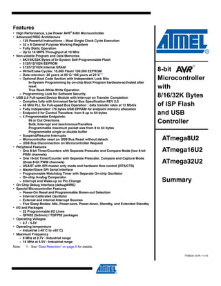
8-bit
Microcontroller
with
8/16/32K Bytes
of ISP Flash
and USB
Controller
ATmega8U2
ATmega16U2
ATmega32U2
Summary
7799DS–AVR–11/10
2. 2
7799DS–AVR–11/10
ATmega8U2/16U2/32U2
1. Pin Configurations
Figure 1-1. Pinout
Note: The large center pad underneath the VQFP and QFN package should be soldered to ground on
the board to ensure good mechanical stability.
1.1 Disclaimer
Typical values contained in this datasheet are based on simulations and characterization of
other AVR microcontrollers manufactured on the same process technology. Min and Max values
will be available after the device is characterized.
UVCC
QFN32(PCINT11 / AIN2 ) PC2
(OC.0B / INT0) PD0
VCC
XTAL1
(INT5/AIN3)PD4
(TXD1/INT3)PD3
(XCK/AIN4/PCINT12)PD5
PB3 (PDO / MISO / PCINT3)
GND
(PC0) XTAL2
UGND
PB4 (T1 / PCINT4)
28 27 26
1
2
3
4
5
6
7
24
23
22
21
20
19
18
1211109 13 14 15
(AIN0 / INT1) PD1
8
16
17
PB6 (PCINT6)
D-
D+
2529303132
PB7 (PCINT7 / OC.0A / OC.1C)
PB5 (PCINT5)
PC7 (INT4 / ICP1 / CLKO)
PC6 (OC.1A / PCINT8)
Reset (PC1 / dW)
PC5(PCINT9/OC.1B)
PC4(PCINT10)
UCAP
(RXD1 / AIN1 / INT2) PD2
(RTS/AIN5/INT6)PD6
(CTS/HWB/AIN6/T0/INT7)PD7
(SS/PCINT0)PB0
(SCLK/PCINT1)PB1
(PDI/MOSI/PCINT2)PB2
AVCC
UVCC
VQFP32(PCINT11 /AIN2 ) PC2
(OC.0B / INT0) PD0
VCC
XTAL1
(INT5/AIN3)PD4
(TXD1/INT3)PD3
(XCKAIN4/PCINT12)PD5
PB3 (PDO / MISO / PCINT3)
GND
(PC0) XTAL2
UGND
PB4 (T1 / PCINT4)
28 27 26
1
2
3
4
5
6
7
24
23
22
21
20
19
18
1211109 13 14 15
(AIN0 / INT1) PD1
8
16
17
PB6 (PCINT6)
D-
D+
2529303132
PB7 (PCINT7 / OC.0A / OC.1C)
PB5 (PCINT5)
PC7 (INT4 / ICP1 / CLKO)
PC6 (OC.1A / PCINT8)
Reset (PC1 / dW)
PC5(PCINT9/OC.1B)
PC4(PCINT10)
UCAP
(RXD1 / AIN1 / INT2) PD2
(RTS/AIN5/INT6)PD6
/HWB/AIN6/T0/INT7)PD7
(SS/PCINT0)PB0
(SCLK/PCINT1)PB1
(PDI/MOSI/PCINT2)PB2
AVCC
3. 3
7799DS–AVR–11/10
ATmega8U2/16U2/32U2
2. Overview
The ATmega8U2/16U2/32U2 is a low-power CMOS 8-bit microcontroller based on the AVR enhanced RISC architecture.
By executing powerful instructions in a single clock cycle, the ATmega8U2/16U2/32U2 achieves throughputs approaching
1 MIPS per MHz allowing the system designer to optimize power consumption versus processing speed.
2.1 Block Diagram
Figure 2-1. Block Diagram
The AVR core combines a rich instruction set with 32 general purpose working registers. All the
32 registers are directly connected to the Arithmetic Logic Unit (ALU), allowing two independent
registers to be accessed in one single instruction executed in one clock cycle. The resulting
PROGRAM
COUNTER
STACK
POINTER
PROGRAM
FLASH
MCU CONTROL
REGISTER
SRAM
GENERAL
PURPOSE
REGISTERS
INSTRUCTION
REGISTER
TIMER/
COUNTERS
INSTRUCTION
DECODER
DATA DIR.
REG. PORTC
DATA REGISTER
PORTC
INTERRUPT
UNIT
EEPROM
USART1
STATUS
REGISTER
Z
Y
X
ALU
PORTC DRIVERSPORTD DRIVERS PORTB DRIVERS
PC7 - PC0PD7 - PD0
RESET
VCC
GND
XTAL1
XTAL2
CONTROL
LINES
ANALOG
COMPARATOR
PB7 - PB0
D+/SCK
D-/SDATA
INTERNAL
OSCILLATOR
WATCHDOG
TIMER
8-BIT DA TA BUS
USB
PS/2
TIMING AND
CONTROL
OSCILLATOR
CALIB. OSC
DATA DIR.
REG. PORTB
DATA REGISTER
PORTB
ON-CHIP DEBUG
Debug-Wire
PROGRAMMING
LOGIC
DATA DIR.
REG. PORTD
DATA REGISTER
PORTD
POR - BOD
RESET
PLL
+
-
SPI
ON-CHIP
3.3V
REGULATOR
UVcc
UCap
1uF
4. 4
7799DS–AVR–11/10
ATmega8U2/16U2/32U2
architecture is more code efficient while achieving throughputs up to ten times faster than con-
ventional CISC microcontrollers.
The ATmega8U2/16U2/32U2 provides the following features: 8K/16K/32K Bytes of In-System
Programmable Flash with Read-While-Write capabilities, 512/512/1024 Bytes EEPROM,
512/512/1024 SRAM, 22 general purpose I/O lines, 32 general purpose working registers, two
flexible Timer/Counters with compare modes and PWM, one USART, a programmable Watch-
dog Timer with Internal Oscillator, an SPI serial port, debugWIRE interface, also used for
accessing the On-chip Debug system and programming and five software selectable power sav-
ing modes. The Idle mode stops the CPU while allowing the SRAM, Timer/Counters, SPI port,
and interrupt system to continue functioning. The Power-down mode saves the register contents
but freezes the Oscillator, disabling all other chip functions until the next interrupt or Hardware
Reset. In Standby mode, the Crystal/Resonator Oscillator is running while the rest of the device
is sleeping. This allows very fast start-up combined with low power consumption. In Extended
Standby mode, the main Oscillator continues to run.
The device is manufactured using Atmel’s high-density nonvolatile memory technology. The on-
chip ISP Flash allows the program memory to be reprogrammed in-system through an SPI serial
interface, by a conventional nonvolatile memory programmer, or by an on-chip Boot program
running on the AVR core. The boot program can use any interface to download the application
program in the application Flash memory. Software in the Boot Flash section will continue to run
while the Application Flash section is updated, providing true Read-While-Write operation. By
combining an 8-bit RISC CPU with In-System Self-Programmable Flash on a monolithic chip,
the Atmel ATmega8U2/16U2/32U2 is a powerful microcontroller that provides a highly flexible
and cost effective solution to many embedded control applications.
The ATmega8U2/16U2/32U2 are supported with a full suite of program and system develop-
ment tools including: C compilers, macro assemblers, program debugger/simulators, in-circuit
emulators, and evaluation kits.
2.2 Pin Descriptions
2.2.1 VCC
Digital supply voltage.
2.2.2 GND
Ground.
2.2.3 AVCC
AVCC is the supply voltage pin (input) for all analog features (Analog Comparator, PLL). It
should be externally connected to VCC through a low-pass filter.
2.2.4 Port B (PB7..PB0)
Port B is an 8-bit bi-directional I/O port with internal pull-up resistors (selected for each bit). The
Port B output buffers have symmetrical drive characteristics with both high sink and source
capability. As inputs, Port B pins that are externally pulled low will source current if the pull-up
resistors are activated. The Port B pins are tri-stated when a reset condition becomes active,
even if the clock is not running.
Port B also serves the functions of various special features of the ATmega8U2/16U2/32U2 as
listed on page 74.
5. 5
7799DS–AVR–11/10
ATmega8U2/16U2/32U2
2.2.5 Port C (PC7..PC0)
Port C is an 8-bit bi-directional I/O port with internal pull-up resistors (selected for each bit). The
Port C output buffers have symmetrical drive characteristics with both high sink and source
capability. As inputs, Port C pins that are externally pulled low will source current if the pull-up
resistors are activated. The Port C pins are tri-stated when a reset condition becomes active,
even if the clock is not running.
Port C also serves the functions of various special features of the ATmega8U2/16U2/32U2 as
listed on page 77.
2.2.6 Port D (PD7..PD0)
Port D serves as analog inputs to the analog comparator.
Port D also serves as an 8-bit bi-directional I/O port, if the analog comparator is not used (con-
cerns PD2/PD1 pins). Port pins can provide internal pull-up resistors (selected for each bit). The
Port D output buffers have symmetrical drive characteristics with both high sink and source
capability. As inputs, Port D pins that are externally pulled low will source current if the pull-up
resistors are activated. The Port D pins are tri-stated when a reset condition becomes active,
even if the clock is not running.
2.2.7 D-
USB Full Speed Negative Data Upstream Port
2.2.8 D+
USB Full Speed Positive Data Upstream Port
2.2.9 UGND
USB Ground.
2.2.10 UVCC
USB Pads Internal Regulator Input supply voltage.
2.2.11 UCAP
USB Pads Internal Regulator Output supply voltage. Should be connected to an external capac-
itor (1µF).
2.2.12 RESET/PC1/dW
Reset input. A low level on this pin for longer than the minimum pulse length will generate a
reset, even if the clock is not running. The minimum pulse length is given in “System Control and
Reset” on page 47. Shorter pulses are not guaranteed to generate a reset. This pin alternatively
serves as debugWire channel or as generic I/O. The configuration depends on the fuses RST-
DISBL and DWEN.
2.2.13 XTAL1
Input to the inverting Oscillator amplifier and input to the internal clock operating circuit.
2.2.14 XTAL2/PC0
Output from the inverting Oscillator amplifier if enabled by Fuse. Also serves as a generic I/O.
6. 6
7799DS–AVR–11/10
ATmega8U2/16U2/32U2
3. Resources
A comprehensive set of development tools, application notes and datasheets are available for
download on http://www.atmel.com/avr.
4. Code Examples
This documentation contains simple code examples that briefly show how to use various parts of
the device. Be aware that not all C compiler vendors include bit definitions in the header files
and interrupt handling in C is compiler dependent. Please confirm with the C compiler documen-
tation for more details.
These code examples assume that the part specific header file is included before compilation.
For I/O registers located in extended I/O map, "IN", "OUT", "SBIS", "SBIC", "CBI", and "SBI"
instructions must be replaced with instructions that allow access to extended I/O. Typically
"LDS" and "STS" combined with "SBRS", "SBRC", "SBR", and "CBR".
5. Data Retention
Reliability Qualification results show that the projected data retention failure rate is much less
than 1 PPM over 20 years at 85°C or 100 years at 25°C.
10. 10
7799DS–AVR–11/10
ATmega8U2/16U2/32U2
Note: 1. For compatibility with future devices, reserved bits should be written to zero if accessed. Moreover reserved bits are not
guaranteed to be read as “0”. Reserved I/O memory addresses should never be written.
2. I/O registers within the address range $00 - $1F are directly bit-accessible using the SBI and CBI instructions. In these reg-
isters, the value of single bits can be checked by using the SBIS and SBIC instructions.
3. Some of the status flags are cleared by writing a logical one to them. Note that the CBI and SBI instructions will operate on
all bits in the I/O register, writing a one back into any flag read as set, thus clearing the flag. The CBI and SBI instructions
work with registers 0x00 to 0x1F only.
4. When using the I/O specific commands IN and OUT, the I/O addresses $00 - $3F must be used. When addressing I/O reg-
isters as data space using LD and ST instructions, $20 must be added to these addresses. The ATmega8U2/16U2/32U2 is
a complex microcontroller with more peripheral units than can be supported within the 64 location reserved in Opcode for
the IN and OUT instructions. For the Extended I/O space from $60 - $1FF in SRAM, only the ST/STS/STD and LD/LDS/LDD
instructions can be used.
0x1A (0x3A) Reserved - - - - - - - -
0x19 (0x39) Reserved - - - - - - - -
0x18 (0x38) Reserved - - - - - - - -
0x17 (0x37) Reserved - - - - - - - -
0x16 (0x36) TIFR1 - - ICF1 - OCF1C OCF1B OCF1A TOV1 page 136
0x15 (0x35) TIFR0 - - - - - OCF0B OCF0A TOV0 page 107
0x14 (0x34) Reserved - - - - - - - -
0x13 (0x33) Reserved - - - - - - - -
0x12 (0x32) Reserved - - - - - - - -
0x11 (0x31) Reserved - - - - - - - -
0x10 (0x30) Reserved - - - - - - - -
0x0F (0x2F) Reserved - - - - - - - -
0x0E (0x2E) Reserved - - - - - - - -
0x0D (0x2D) Reserved - - - - - - - -
0x0C (0x2C) Reserved - - - - - - - -
0x0B (0x2B) PORTD PORTD7 PORTD6 PORTD5 PORTD4 PORTD3 PORTD2 PORTD1 PORTD0 page 83
0x0A (0x2A) DDRD DDD7 DDD6 DDD5 DDD4 DDD3 DDD2 DDD1 DDD0 page 83
0x09 (0x29) PIND PIND7 PIND6 PIND5 PIND4 PIND3 PIND2 PIND1 PIND0 page 83
0x08 (0x28) PORTC PORTC7 PORTC6 PORTC5 PORTC4 - PORTC2 PORTC1 PORTC0 page 82
0x07 (0x27) DDRC DDC7 DDC6 DDC5 DDC4 - DDC2 DDC1 DDC0 page 82
0x06 (0x26) PINC PINC7 PINC6 PINC5 PINC4 - PINC2 PINC1 PINC0 page 82
0x05 (0x25) PORTB PORTB7 PORTB6 PORTB5 PORTB4 PORTB3 PORTB2 PORTB1 PORTB0 page 82
0x04 (0x24) DDRB DDB7 DDB6 DDB5 DDB4 DDB3 DDB2 DDB1 DDB0 page 82
0x03 (0x23) PINB PINB7 PINB6 PINB5 PINB4 PINB3 PINB2 PINB1 PINB0 page 82
0x02 (0x22) Reserved - - - - - - - -
0x01 (0x21) Reserved - - - - - - - -
0x00 (0x20) Reserved - - - - - - - -
Address Name Bit 7 Bit 6 Bit 5 Bit 4 Bit 3 Bit 2 Bit 1 Bit 0 Page
11. 11
7799DS–AVR–11/10
ATmega8U2/16U2/32U2
7. Instruction Set Summary
Mnemonics Operands Description Operation Flags #Clocks
ARITHMETIC AND LOGIC INSTRUCTIONS
ADD Rd, Rr Add two Registers Rd ← Rd + Rr Z,C,N,V,H 1
ADC Rd, Rr Add with Carry two Registers Rd ← Rd + Rr + C Z,C,N,V,H 1
ADIW Rdl,K Add Immediate to Word Rdh:Rdl ← Rdh:Rdl + K Z,C,N,V,S 2
SUB Rd, Rr Subtract two Registers Rd ← Rd - Rr Z,C,N,V,H 1
SUBI Rd, K Subtract Constant from Register Rd ← Rd - K Z,C,N,V,H 1
SBC Rd, Rr Subtract with Carry two Registers Rd ← Rd - Rr - C Z,C,N,V,H 1
SBCI Rd, K Subtract with Carry Constant from Reg. Rd ← Rd - K - C Z,C,N,V,H 1
SBIW Rdl,K Subtract Immediate from Word Rdh:Rdl ← Rdh:Rdl - K Z,C,N,V,S 2
AND Rd, Rr Logical AND Registers Rd ← Rd • Rr Z,N,V 1
ANDI Rd, K Logical AND Register and Constant Rd ← Rd • K Z,N,V 1
OR Rd, Rr Logical OR Registers Rd ← Rd v Rr Z,N,V 1
ORI Rd, K Logical OR Register and Constant Rd ← Rd v K Z,N,V 1
EOR Rd, Rr Exclusive OR Registers Rd ← Rd ⊕ Rr Z,N,V 1
COM Rd One’s Complement Rd ← 0xFF − Rd Z,C,N,V 1
NEG Rd Two’s Complement Rd ← 0x00 − Rd Z,C,N,V,H 1
SBR Rd,K Set Bit(s) in Register Rd ← Rd v K Z,N,V 1
CBR Rd,K Clear Bit(s) in Register Rd ← Rd • (0xFF - K) Z,N,V 1
INC Rd Increment Rd ← Rd + 1 Z,N,V 1
DEC Rd Decrement Rd ← Rd − 1 Z,N,V 1
TST Rd Test for Zero or Minus Rd ← Rd • Rd Z,N,V 1
CLR Rd Clear Register Rd ← Rd ⊕ Rd Z,N,V 1
SER Rd Set Register Rd ← 0xFF None 1
BRANCH INSTRUCTIONS
RJMP k Relative Jump PC ← PC + k + 1 None 2
IJMP Indirect Jump to (Z) PC ← Z None 2
JMP k Direct Jump PC ← k None 3
RCALL k Relative Subroutine Call PC ← PC + k + 1 None 4
ICALL Indirect Call to (Z) PC ← Z None 4
CALL k Direct Subroutine Call PC ← k None 5
RET Subroutine Return PC ← STACK None 5
RETI Interrupt Return PC ← STACK I 5
CPSE Rd,Rr Compare, Skip if Equal if (Rd = Rr) PC ← PC + 2 or 3 None 1/2/3
CP Rd,Rr Compare Rd − Rr Z, N,V,C,H 1
CPC Rd,Rr Compare with Carry Rd − Rr − C Z, N,V,C,H 1
CPI Rd,K Compare Register with Immediate Rd − K Z, N,V,C,H 1
SBRC Rr, b Skip if Bit in Register Cleared if (Rr(b)=0) PC ← PC + 2 or 3 None 1/2/3
SBRS Rr, b Skip if Bit in Register is Set if (Rr(b)=1) PC ← PC + 2 or 3 None 1/2/3
SBIC P, b Skip if Bit in I/O Register Cleared if (P(b)=0) PC ← PC + 2 or 3 None 1/2/3
SBIS P, b Skip if Bit in I/O Register is Set if (P(b)=1) PC ← PC + 2 or 3 None 1/2/3
BRBS s, k Branch if Status Flag Set if (SREG(s) = 1) then PC←PC+k + 1 None 1/2
BRBC s, k Branch if Status Flag Cleared if (SREG(s) = 0) then PC←PC+k + 1 None 1/2
BREQ k Branch if Equal if (Z = 1) then PC ← PC + k + 1 None 1/2
BRNE k Branch if Not Equal if (Z = 0) then PC ← PC + k + 1 None 1/2
BRCS k Branch if Carry Set if (C = 1) then PC ← PC + k + 1 None 1/2
BRCC k Branch if Carry Cleared if (C = 0) then PC ← PC + k + 1 None 1/2
BRSH k Branch if Same or Higher if (C = 0) then PC ← PC + k + 1 None 1/2
BRLO k Branch if Lower if (C = 1) then PC ← PC + k + 1 None 1/2
BRMI k Branch if Minus if (N = 1) then PC ← PC + k + 1 None 1/2
BRPL k Branch if Plus if (N = 0) then PC ← PC + k + 1 None 1/2
BRGE k Branch if Greater or Equal, Signed if (N ⊕ V= 0) then PC ← PC + k + 1 None 1/2
BRLT k Branch if Less Than Zero, Signed if (N ⊕ V= 1) then PC ← PC + k + 1 None 1/2
BRHS k Branch if Half Carry Flag Set if (H = 1) then PC ← PC + k + 1 None 1/2
BRHC k Branch if Half Carry Flag Cleared if (H = 0) then PC ← PC + k + 1 None 1/2
BRTS k Branch if T Flag Set if (T = 1) then PC ← PC + k + 1 None 1/2
BRTC k Branch if T Flag Cleared if (T = 0) then PC ← PC + k + 1 None 1/2
BRVS k Branch if Overflow Flag is Set if (V = 1) then PC ← PC + k + 1 None 1/2
BRVC k Branch if Overflow Flag is Cleared if (V = 0) then PC ← PC + k + 1 None 1/2
BRIE k Branch if Interrupt Enabled if ( I = 1) then PC ← PC + k + 1 None 1/2
BRID k Branch if Interrupt Disabled if ( I = 0) then PC ← PC + k + 1 None 1/2
BIT AND BIT-TEST INSTRUCTIONS
SBI P,b Set Bit in I/O Register I/O(P,b) ← 1 None 2
CBI P,b Clear Bit in I/O Register I/O(P,b) ← 0 None 2
LSL Rd Logical Shift Left Rd(n+1) ← Rd(n), Rd(0) ← 0 Z,C,N,V 1
LSR Rd Logical Shift Right Rd(n) ← Rd(n+1), Rd(7) ← 0 Z,C,N,V 1
12. 12
7799DS–AVR–11/10
ATmega8U2/16U2/32U2
ROL Rd Rotate Left Through Carry Rd(0)←C,Rd(n+1)← Rd(n),C←Rd(7) Z,C,N,V 1
ROR Rd Rotate Right Through Carry Rd(7)←C,Rd(n)← Rd(n+1),C←Rd(0) Z,C,N,V 1
ASR Rd Arithmetic Shift Right Rd(n) ← Rd(n+1), n=0..6 Z,C,N,V 1
SWAP Rd Swap Nibbles Rd(3..0)←Rd(7..4),Rd(7..4)←Rd(3..0) None 1
BSET s Flag Set SREG(s) ← 1 SREG(s) 1
BCLR s Flag Clear SREG(s) ← 0 SREG(s) 1
BST Rr, b Bit Store from Register to T T ← Rr(b) T 1
BLD Rd, b Bit load from T to Register Rd(b) ← T None 1
SEC Set Carry C ← 1 C 1
CLC Clear Carry C ← 0 C 1
SEN Set Negative Flag N ← 1 N 1
CLN Clear Negative Flag N ← 0 N 1
SEZ Set Zero Flag Z ← 1 Z 1
CLZ Clear Zero Flag Z ← 0 Z 1
SEI Global Interrupt Enable I ← 1 I 1
CLI Global Interrupt Disable I ← 0 I 1
SES Set Signed Test Flag S ← 1 S 1
CLS Clear Signed Test Flag S ← 0 S 1
SEV Set Twos Complement Overflow. V ← 1 V 1
CLV Clear Twos Complement Overflow V ← 0 V 1
SET Set T in SREG T ← 1 T 1
CLT Clear T in SREG T ← 0 T 1
SEH Set Half Carry Flag in SREG H ← 1 H 1
CLH Clear Half Carry Flag in SREG H ← 0 H 1
DATA TRANSFER INSTRUCTIONS
MOV Rd, Rr Move Between Registers Rd ← Rr None 1
MOVW Rd, Rr Copy Register Word Rd+1:Rd ← Rr+1:Rr None 1
LDI Rd, K Load Immediate Rd ← K None 1
LD Rd, X Load Indirect Rd ← (X) None 2
LD Rd, X+ Load Indirect and Post-Inc. Rd ← (X), X ← X + 1 None 2
LD Rd, - X Load Indirect and Pre-Dec. X ← X - 1, Rd ← (X) None 2
LD Rd, Y Load Indirect Rd ← (Y) None 2
LD Rd, Y+ Load Indirect and Post-Inc. Rd ← (Y), Y ← Y + 1 None 2
LD Rd, - Y Load Indirect and Pre-Dec. Y ← Y - 1, Rd ← (Y) None 2
LDD Rd,Y+q Load Indirect with Displacement Rd ← (Y + q) None 2
LD Rd, Z Load Indirect Rd ← (Z) None 2
LD Rd, Z+ Load Indirect and Post-Inc. Rd ← (Z), Z ← Z+1 None 2
LD Rd, -Z Load Indirect and Pre-Dec. Z ← Z - 1, Rd ← (Z) None 2
LDD Rd, Z+q Load Indirect with Displacement Rd ← (Z + q) None 2
LDS Rd, k Load Direct from SRAM Rd ← (k) None 2
ST X, Rr Store Indirect (X) ← Rr None 2
ST X+, Rr Store Indirect and Post-Inc. (X) ← Rr, X ← X + 1 None 2
ST - X, Rr Store Indirect and Pre-Dec. X ← X - 1, (X) ← Rr None 2
ST Y, Rr Store Indirect (Y) ← Rr None 2
ST Y+, Rr Store Indirect and Post-Inc. (Y) ← Rr, Y ← Y + 1 None 2
ST - Y, Rr Store Indirect and Pre-Dec. Y ← Y - 1, (Y) ← Rr None 2
STD Y+q,Rr Store Indirect with Displacement (Y + q) ← Rr None 2
ST Z, Rr Store Indirect (Z) ← Rr None 2
ST Z+, Rr Store Indirect and Post-Inc. (Z) ← Rr, Z ← Z + 1 None 2
ST -Z, Rr Store Indirect and Pre-Dec. Z ← Z - 1, (Z) ← Rr None 2
STD Z+q,Rr Store Indirect with Displacement (Z + q) ← Rr None 2
STS k, Rr Store Direct to SRAM (k) ← Rr None 2
LPM Load Program Memory R0 ← (Z) None 3
LPM Rd, Z Load Program Memory Rd ← (Z) None 3
LPM Rd, Z+ Load Program Memory and Post-Inc Rd ← (Z), Z ← Z+1 None 3
SPM Store Program Memory (Z) ← R1:R0 None -
IN Rd, P In Port Rd ← P None 1
OUT P, Rr Out Port P ← Rr None 1
PUSH Rr Push Register on Stack STACK ← Rr None 2
POP Rd Pop Register from Stack Rd ← STACK None 2
MCU CONTROL INSTRUCTIONS
NOP No Operation None 1
SLEEP Sleep (see specific descr. for Sleep function) None 1
WDR Watchdog Reset (see specific descr. for WDR/timer) None 1
BREAK Break For On-chip Debug Only None N/A
Mnemonics Operands Description Operation Flags #Clocks
13. 13
7799DS–AVR–11/10
ATmega8U2/16U2/32U2
8. Ordering Information
8.1 ATmega8U2
Speed Power Supply Ordering Code Package Operational Range
16 MHz 2.7 - 5.5V
ATmega8U2-AU 32A
-40°C to +85°C
ATmega8U2-MU 32M1-A
Package Type
32A 32-lead, 7 x7 x 1.2 mm, lead pitch 0.8 mm Thin Quad Flat Package
32M1 32-pad, 5 x 5 x 1 mm body, pad pitch 0.50 mm Quad Flat No lead (QFN)
14. 14
7799DS–AVR–11/10
ATmega8U2/16U2/32U2
8.2 ATmega16U2
Speed Power Supply Ordering Code Package Operational Range
16 MHz 2.7 - 5.5V
ATmega16U2-AU 32A
-40°C to +85°C
ATmega16U2-MU 32M1-A
Package Type
32A 32-lead, 7 x7 x 1.2 mm, lead pitch 0.8 mm Thin Quad Flat Package
32M1 32-pad, 5 x 5 x 1 mm body, pad pitch 0.50 mm Quad Flat No lead (QFN)
15. 15
7799DS–AVR–11/10
ATmega8U2/16U2/32U2
8.3 ATmega32U2
Speed Power Supply Ordering Code Package Operational Range
16 MHz 2.7 - 5.5V
ATmega32U2-AU 32A
-40°C to +85°C
ATmega32U2-MU 32M1-A
Package Type
32A 32-lead, 7 x7 x 1.2 mm, lead pitch 0.8 mm Thin Quad Flat Package
32M1 32-pad, 5 x 5 x 1 mm body, pad pitch 0.50 mm Quad Flat No lead (QFN)
18. 18
7799DS–AVR–11/10
ATmega8U2/16U2/32U2
10. Errata
10.1 Errata ATmega8U2
The revision letter in this section refers to the revision of the ATmega8U2 device.
10.1.1 rev. A and rev B
• Full Swing oscillator
1. Full Swing oscillator
The maximum frequency for the Full Swing Crystal Oscillator is 8MHz. For Crystal frequen-
cies > 8MHz the Full Swing Crystal Oscillator is not guaranteed to operate correctly.
Problem fix/Workaround
If a Crystal with frequency > 8MHz is used, the Low Power Crystal Oscillator option should
be used instead. See table 8-1 for an overview of the Device Clocking Options. Note that the
Low Power Crystal Oscillator will not provide full rail-to-rail swing on the XTAL2 pin. If sys-
tem clock output is needed to drive other clock inputs while running from the Low Power
Crystal Oscillator, the system clock can be output on PORTC7 by programming the CKOUT
fuse.
10.2 Errata ATmega16U2
The revision letter in this section refers to the revision of the ATmega16U2 device.
10.2.1 rev. A and rev B
• Full Swing oscillator
1. Full Swing oscillator
The maximum frequency for the Full Swing Crystal Oscillator is 8MHz. For Crystal frequen-
cies > 8MHz the Full Swing Crystal Oscillator is not guaranteed to operate correctly.
Problem fix/Workaround
If a Crystal with frequency > 8MHz is used, the Low Power Crystal Oscillator option should
be used instead. See table 8-1 for an overview of the Device Clocking Options. Note that the
Low Power Crystal Oscillator will not provide full rail-to-rail swing on the XTAL2 pin. If sys-
tem clock output is needed to drive other clock inputs while running from the Low Power
Crystal Oscillator, the system clock can be output on PORTC7 by programming the CKOUT
fuse.
10.3 Errata ATmega32U2
The revision letter in this section refers to the revision of the ATmega32U2 device.
10.3.1 rev. C
No Known Errata
19. 19
7799DS–AVR–11/10
ATmega8U2/16U2/32U2
10.3.2 rev. A and rev B
• Full Swing oscillator
1. Full Swing oscillator
The maximum frequency for the Full Swing Crystal Oscillator is 8MHz. For Crystal frequen-
cies > 8MHz the Full Swing Crystal Oscillator is not guaranteed to operate correctly.
Problem fix/Workaround
If a Crystal with frequency > 8MHz is used, the Low Power Crystal Oscillator option should
be used instead. See table 8-1 for an overview of the Device Clocking Options. Note that the
Low Power Crystal Oscillator will not provide full rail-to-rail swing on the XTAL2 pin. If sys-
tem clock output is needed to drive other clock inputs while running from the Low Power
Crystal Oscillator, the system clock can be output on PORTC7 by programming the CKOUT
fuse.
20. 20
7799DS–AVR–11/10
ATmega8U2/16U2/32U2
11. Datasheet Revision History
Please note that the referring page numbers in this section are referred to this document. The
referring revision in this section are referring to the document revision.
11.1 Rev. 7799D – 11/10
11.2 Rev. 7799C – 12/09
11.3 Rev. 7799B – 06/09
11.4 Rev. 7799A – 03/09
1. Updated the footnote on page 2. Removed the VQFP from the footnote
2. Updated Section 20-4 ”Typical Bus powered application with 3.3V I/O” on page 187.
3. Updated Figure 20-6 on page 188. By connecting UVCC to 3V power-supply.
4. Updated Table 21-2 on page 215. 10: Bulk Type, and 01: Isochronous Type
5. Added UVCC limits in Electrical Characteristics
6.
Updated “Electrical Characteristics” on page 264. Added USB D+ Internal Pull-up (streaming
mode)
7. Updated “Register Summary” on page 288. Added DIDR1 (adress: 0x7F)
8. Removed Figure 27-26: USB Regulator Consumption with load 75Ω vs. Vcc
1. Updated “Features” on page 1.
2. Added description of “AVCC” on page 4.
3. Updated Figure 7-2 on page 18.
4. Updated Figure 20-3 on page 186 and Figure 20-4 on page 187.
5. Updated “Fuse Bits” on page 247.
6. Updated “DC Characteristics” on page 264.
7. Updated Table 26-3 on page 267, by removing Vrst.
8. Updated Table 26-4 on page 268.
9. Updated “Typical Characteristics” on page 273.
10. Added new “Errata” on page 299.
1. Updated “Typical Characteristics” on page 273.
1. Initial revision.