SlideShare ist ein Scribd-Unternehmen logo
1 von 36
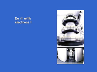
Do it with
electrons !
Microscopy
Structure determines properties
We have discussed crystal structure (x-ray diffraction)
But consider now different level of structure
Microstructure (微观结构)- also affects properties
Grey cast iron (灰色生铁) -
rather brittle
Ductile iron - highly ductile
Microscopy
Structure determines properties
We have discussed crystal structure (x-ray diffraction)
But consider now different level of structure
Microstructure - also affects properties
Cemented WC (碳化钨)
cutting tool
Microscopy
Structure determines properties
We have discussed crystal structure (x-ray diffraction)
But consider now different level of structure
Microstructure - also affects properties
Ferroelectric domains in BaTiO3
Microscopy
Structure determines properties
We have discussed crystal structure (x-ray diffraction)
But consider now different level of structure
Microstructure - also can be 'art (美术)'
Electron microscopy
SEM - scanning electron microscopy
tiny electron beam scanned across surface of specimen
backscattered (背散射) or
secondary electrons (二次电子) detected
signal output to synchronized display
Electron microscopy
SEM - scanning electron microscopy
Magnification range 15x to 200,000x
Resolution of 50 Å
Excellent depth of focus
Relatively easy sample prep
SEM - scanning electron microscopy
Electron gun
Don't make x-rays - use
electrons directly
Wavelength:
NOT  = hc/E
(massless photons)
 = h/(2melectronqVo)1/2
(non-relativistic)
 = h/(2melectronqVo + q2Vo
2/c2)1/2
(relativistic (相对论的))
SEM - scanning electron microscopy
 = h / (2melectronqVo + q2Vo
2/c2)1/2
 = 1.22639 / (Vo + 0.97845 · 10-6Vo
2)1/2
(nm) & Vo(volts)
10 kV ——> 0.12 Å
100 kV ——> 0.037 Å
SEM - scanning electron microscopy
Wehnelt
SEM - scanning electron microscopy
Electron gun
Electron emitter
SEM - scanning electron microscopy
Effects of increasing voltage in
electron gun:
Resolution increased (
decreased)
Penetration increases
Specimen charging increases
(insulators)
Specimen damage increases
Image contrast decreases
 = h/(2melectronqVo + q2Vo2/c2))1/2
SEM - scanning electron microscopy
Field emission electron source:
High electric field at very sharp tip causes electrons to "tunnel"
maybe
SEM - scanning electron microscopy
Field emission electron source:
High electric field at very sharp tip causes electrons to "tunnel"
SEM - scanning electron microscopy
Field emission electron source:
High electric field at very sharp tip causes electrons to "tunnel"
cool tip ——> smaller E in beam
improved coherence
many electrons from small tip ——> finer
probe size, higher current densities (100X >)
problems - high vacuum, more $$$, fussy
SEM - scanning electron microscopy
Lenses
electrons focused by Lorentz force from electromagnetic field
F = qv x B
effectively same as optical lenses
Lenses are ring-shaped
coils generate magnetic field
electrons pass thru hollow center
lens focal length is continuously variable
apertures control, limit beam
SEM - scanning electron microscopy
Specimen
Conducting -
little or no preparation
attach to mounting stub
for insertion into
instrument
may need to provide
conductive path with
Ag paint
Non-conducting -
usually coat with conductive very thin layer (Au, C, Cr)
SEM - scanning electron microscopy
Specimen
Can examine
fracture surfaces
electronic devices
fibers
coatings
particles
etc.
SEM - scanning electron microscopy
Specimen
Can be tilted, translated
Specimen size limited by
size of sample chamber
SEM - scanning electron microscopy
Specimen
What comes from specimen?
Backscattered electrons
Secondary electrons
Fluorescent X-rays
high energy
compositional contrast
low energy
topographic contrast
composition - EDS
Brightness of regions in image
increases as atomic number increases
(less penetration gives more
backscattered electrons)
SEM - scanning electron microscopy
Electron energy distribution
BSEs
SEs
E/Eo
1
SEM - scanning electron microscopy
Backscattered electron detector - solid state detector
electron energy up to 30-50 keV
annular around incident beam
repel secondary electrons with
— biased mesh
images are more sensitive to
chemical composition (electron
yield depends on atomic number)
line of sight necessary
SEM - scanning electron microscopy
Secondary electron detector - scintillation detector
+ bias mesh needed in front of
detector to attract low energy
electrons
line of sight unnecessary
SEM - scanning electron microscopy
Secondary electron detector - scintillation detector
SEM - scanning electron microscopy
Choose correct detector- topography example
Fracture surface in iron
backscattered electrons secondary electrons
SEM - scanning electron microscopy
Composition - what elements present at a particular spot in specimen?
Use solid state detector
Do energy scan for fluorescent X-rays
SEM - scanning electron microscopy
Composition mapping - x-ray fluorescence
Use solid state detector set for X-ray energy for a
particular element in specimen
image X-ray map
SEM - scanning electron microscopy
Interaction volume
Backscattered electrons
come from whole volume
(high energy)
Secondary electrons come
from neck only (low energy)
SEM - scanning electron microscopy
Contrast
Comes from any kind of interaction with electron beam
topography
composition
elements
phases
grain (crystal) orientation
charging affects contrast
SEM - scanning electron microscopy
Magnification
SEM - scanning electron microscopy
Resolution
Determined by
probe size
SEM - scanning electron microscopy
Resolution
Determined by
probe size
SEM - scanning electron microscopy
Depth of field
d = depth of field
 = required spatial resolution
a = convergence angle

d
region of image in focus
tana 
0.5
0.5d


d
For small angles, tana = a
d 

a
Can control depth of field (d) with convergence angle (a)
SEM - scanning electron microscopy
Depth of field
WD
Rap
tan a 
Rap
WD

Weitere ähnliche Inhalte

Ähnlich wie SEM.ppt

Transmission Electron Microscope
Transmission Electron MicroscopeTransmission Electron Microscope
Transmission Electron MicroscopeManoranjan Ghosh
 
Scanning Electron Microscopy (SEM) Analysis.pdf
Scanning Electron Microscopy (SEM) Analysis.pdfScanning Electron Microscopy (SEM) Analysis.pdf
Scanning Electron Microscopy (SEM) Analysis.pdfSanDeepSharma926061
 
Scanning Electron Microscope.pptx
Scanning Electron Microscope.pptxScanning Electron Microscope.pptx
Scanning Electron Microscope.pptxRABEYABASORI
 
Microprobing with electrons
Microprobing with electronsMicroprobing with electrons
Microprobing with electronsJonathan Price
 
Scanning Electron Microscopy (SEM 2013).pptx
Scanning Electron Microscopy (SEM 2013).pptxScanning Electron Microscopy (SEM 2013).pptx
Scanning Electron Microscopy (SEM 2013).pptxAryaSehrawat1
 
Scanning Electron Microscopy
Scanning Electron MicroscopyScanning Electron Microscopy
Scanning Electron MicroscopySejal9787
 
Transmission electron microscopy-TEM, principle and working.pptx
Transmission electron microscopy-TEM, principle and working.pptxTransmission electron microscopy-TEM, principle and working.pptx
Transmission electron microscopy-TEM, principle and working.pptxav1574
 
ELECTRON MICROSCOPY (TEM & SEM)
ELECTRON MICROSCOPY (TEM & SEM)ELECTRON MICROSCOPY (TEM & SEM)
ELECTRON MICROSCOPY (TEM & SEM)ADITYA ARYA
 
Advanced Characterization Technique - SEM
Advanced Characterization Technique - SEMAdvanced Characterization Technique - SEM
Advanced Characterization Technique - SEMIlyas Hussain
 
xray production.pptx
xray production.pptxxray production.pptx
xray production.pptxAtul Verma
 
Scanning electron microscope
Scanning electron microscopeScanning electron microscope
Scanning electron microscopeSenthil Arasan
 
SCANNING ELECTRON MICROSCOPE MITHILESH CHOUDHARY
SCANNING ELECTRON MICROSCOPE MITHILESH CHOUDHARYSCANNING ELECTRON MICROSCOPE MITHILESH CHOUDHARY
SCANNING ELECTRON MICROSCOPE MITHILESH CHOUDHARYAnjan Anant
 
Characterization of nanoparticles
Characterization of nanoparticlesCharacterization of nanoparticles
Characterization of nanoparticlesAnil Pethe
 
Swift Heavy Ion Irradiation
Swift Heavy Ion IrradiationSwift Heavy Ion Irradiation
Swift Heavy Ion Irradiationkrishslide
 

Ähnlich wie SEM.ppt (20)

Transmission Electron Microscope
Transmission Electron MicroscopeTransmission Electron Microscope
Transmission Electron Microscope
 
Scanning Electron Microscopy (SEM) Analysis.pdf
Scanning Electron Microscopy (SEM) Analysis.pdfScanning Electron Microscopy (SEM) Analysis.pdf
Scanning Electron Microscopy (SEM) Analysis.pdf
 
Scanning Electron Microscope.pptx
Scanning Electron Microscope.pptxScanning Electron Microscope.pptx
Scanning Electron Microscope.pptx
 
Microscoy description by praveen
Microscoy description by praveenMicroscoy description by praveen
Microscoy description by praveen
 
Microprobing with electrons
Microprobing with electronsMicroprobing with electrons
Microprobing with electrons
 
GenerationofXRays.ppt
GenerationofXRays.pptGenerationofXRays.ppt
GenerationofXRays.ppt
 
SEM-for MS.pptx
SEM-for MS.pptxSEM-for MS.pptx
SEM-for MS.pptx
 
Scanning Electron Microscope
Scanning Electron MicroscopeScanning Electron Microscope
Scanning Electron Microscope
 
Sem md ppt
Sem md pptSem md ppt
Sem md ppt
 
Scanning Electron Microscopy (SEM 2013).pptx
Scanning Electron Microscopy (SEM 2013).pptxScanning Electron Microscopy (SEM 2013).pptx
Scanning Electron Microscopy (SEM 2013).pptx
 
Scanning Electron Microscopy
Scanning Electron MicroscopyScanning Electron Microscopy
Scanning Electron Microscopy
 
Transmission electron microscopy-TEM, principle and working.pptx
Transmission electron microscopy-TEM, principle and working.pptxTransmission electron microscopy-TEM, principle and working.pptx
Transmission electron microscopy-TEM, principle and working.pptx
 
ELECTRON MICROSCOPY (TEM & SEM)
ELECTRON MICROSCOPY (TEM & SEM)ELECTRON MICROSCOPY (TEM & SEM)
ELECTRON MICROSCOPY (TEM & SEM)
 
Sem Poster
Sem PosterSem Poster
Sem Poster
 
Advanced Characterization Technique - SEM
Advanced Characterization Technique - SEMAdvanced Characterization Technique - SEM
Advanced Characterization Technique - SEM
 
xray production.pptx
xray production.pptxxray production.pptx
xray production.pptx
 
Scanning electron microscope
Scanning electron microscopeScanning electron microscope
Scanning electron microscope
 
SCANNING ELECTRON MICROSCOPE MITHILESH CHOUDHARY
SCANNING ELECTRON MICROSCOPE MITHILESH CHOUDHARYSCANNING ELECTRON MICROSCOPE MITHILESH CHOUDHARY
SCANNING ELECTRON MICROSCOPE MITHILESH CHOUDHARY
 
Characterization of nanoparticles
Characterization of nanoparticlesCharacterization of nanoparticles
Characterization of nanoparticles
 
Swift Heavy Ion Irradiation
Swift Heavy Ion IrradiationSwift Heavy Ion Irradiation
Swift Heavy Ion Irradiation
 

Mehr von MuhammadJavedIqbal40 (19)

Presentation (4).pptx
Presentation (4).pptxPresentation (4).pptx
Presentation (4).pptx
 
ANOVA 2023 aa 2564896.pptx
ANOVA 2023  aa 2564896.pptxANOVA 2023  aa 2564896.pptx
ANOVA 2023 aa 2564896.pptx
 
qualityassuranceppt-06072023.pptx
qualityassuranceppt-06072023.pptxqualityassuranceppt-06072023.pptx
qualityassuranceppt-06072023.pptx
 
Quali.pdf
Quali.pdfQuali.pdf
Quali.pdf
 
BET.pptx
BET.pptxBET.pptx
BET.pptx
 
Alkene and alkyne 2nd semester 2023.pptx
Alkene and alkyne 2nd semester 2023.pptxAlkene and alkyne 2nd semester 2023.pptx
Alkene and alkyne 2nd semester 2023.pptx
 
Alkynes2.ppt
Alkynes2.pptAlkynes2.ppt
Alkynes2.ppt
 
DSC.pdf
DSC.pdfDSC.pdf
DSC.pdf
 
Photoluminescence -chapter-6.pdf
Photoluminescence -chapter-6.pdfPhotoluminescence -chapter-6.pdf
Photoluminescence -chapter-6.pdf
 
Photoluminescence.pptx
Photoluminescence.pptxPhotoluminescence.pptx
Photoluminescence.pptx
 
organic-chemistry-2nd semester 2023.pptx
organic-chemistry-2nd semester 2023.pptxorganic-chemistry-2nd semester 2023.pptx
organic-chemistry-2nd semester 2023.pptx
 
Fluoroscence 1.pptx
Fluoroscence 1.pptxFluoroscence 1.pptx
Fluoroscence 1.pptx
 
Notes- Organic day 2.pptx
Notes- Organic day 2.pptxNotes- Organic day 2.pptx
Notes- Organic day 2.pptx
 
thermodynamics PNC.ppt
thermodynamics PNC.pptthermodynamics PNC.ppt
thermodynamics PNC.ppt
 
1606732404-atomic-absorption-emission-2.ppt
1606732404-atomic-absorption-emission-2.ppt1606732404-atomic-absorption-emission-2.ppt
1606732404-atomic-absorption-emission-2.ppt
 
PNC IIIA group 2023.pptx
PNC IIIA group 2023.pptxPNC IIIA group 2023.pptx
PNC IIIA group 2023.pptx
 
interhalogens pseudohalogen PNC.pptx
interhalogens  pseudohalogen  PNC.pptxinterhalogens  pseudohalogen  PNC.pptx
interhalogens pseudohalogen PNC.pptx
 
PNC IIA group 2023.pptx
PNC IIA group 2023.pptxPNC IIA group 2023.pptx
PNC IIA group 2023.pptx
 
Group 13, the Boron family.ppt
Group 13, the Boron family.pptGroup 13, the Boron family.ppt
Group 13, the Boron family.ppt
 

Kürzlich hochgeladen

microwave assisted reaction. General introduction
microwave assisted reaction. General introductionmicrowave assisted reaction. General introduction
microwave assisted reaction. General introductionMaksud Ahmed
 
Grant Readiness 101 TechSoup and Remy Consulting
Grant Readiness 101 TechSoup and Remy ConsultingGrant Readiness 101 TechSoup and Remy Consulting
Grant Readiness 101 TechSoup and Remy ConsultingTechSoup
 
Employee wellbeing at the workplace.pptx
Employee wellbeing at the workplace.pptxEmployee wellbeing at the workplace.pptx
Employee wellbeing at the workplace.pptxNirmalaLoungPoorunde1
 
“Oh GOSH! Reflecting on Hackteria's Collaborative Practices in a Global Do-It...
“Oh GOSH! Reflecting on Hackteria's Collaborative Practices in a Global Do-It...“Oh GOSH! Reflecting on Hackteria's Collaborative Practices in a Global Do-It...
“Oh GOSH! Reflecting on Hackteria's Collaborative Practices in a Global Do-It...Marc Dusseiller Dusjagr
 
URLs and Routing in the Odoo 17 Website App
URLs and Routing in the Odoo 17 Website AppURLs and Routing in the Odoo 17 Website App
URLs and Routing in the Odoo 17 Website AppCeline George
 
Separation of Lanthanides/ Lanthanides and Actinides
Separation of Lanthanides/ Lanthanides and ActinidesSeparation of Lanthanides/ Lanthanides and Actinides
Separation of Lanthanides/ Lanthanides and ActinidesFatimaKhan178732
 
Sanyam Choudhary Chemistry practical.pdf
Sanyam Choudhary Chemistry practical.pdfSanyam Choudhary Chemistry practical.pdf
Sanyam Choudhary Chemistry practical.pdfsanyamsingh5019
 
CARE OF CHILD IN INCUBATOR..........pptx
CARE OF CHILD IN INCUBATOR..........pptxCARE OF CHILD IN INCUBATOR..........pptx
CARE OF CHILD IN INCUBATOR..........pptxGaneshChakor2
 
Paris 2024 Olympic Geographies - an activity
Paris 2024 Olympic Geographies - an activityParis 2024 Olympic Geographies - an activity
Paris 2024 Olympic Geographies - an activityGeoBlogs
 
Industrial Policy - 1948, 1956, 1973, 1977, 1980, 1991
Industrial Policy - 1948, 1956, 1973, 1977, 1980, 1991Industrial Policy - 1948, 1956, 1973, 1977, 1980, 1991
Industrial Policy - 1948, 1956, 1973, 1977, 1980, 1991RKavithamani
 
Q4-W6-Restating Informational Text Grade 3
Q4-W6-Restating Informational Text Grade 3Q4-W6-Restating Informational Text Grade 3
Q4-W6-Restating Informational Text Grade 3JemimahLaneBuaron
 
BASLIQ CURRENT LOOKBOOK LOOKBOOK(1) (1).pdf
BASLIQ CURRENT LOOKBOOK  LOOKBOOK(1) (1).pdfBASLIQ CURRENT LOOKBOOK  LOOKBOOK(1) (1).pdf
BASLIQ CURRENT LOOKBOOK LOOKBOOK(1) (1).pdfSoniaTolstoy
 
Introduction to AI in Higher Education_draft.pptx
Introduction to AI in Higher Education_draft.pptxIntroduction to AI in Higher Education_draft.pptx
Introduction to AI in Higher Education_draft.pptxpboyjonauth
 
Z Score,T Score, Percential Rank and Box Plot Graph
Z Score,T Score, Percential Rank and Box Plot GraphZ Score,T Score, Percential Rank and Box Plot Graph
Z Score,T Score, Percential Rank and Box Plot GraphThiyagu K
 
Organic Name Reactions for the students and aspirants of Chemistry12th.pptx
Organic Name Reactions  for the students and aspirants of Chemistry12th.pptxOrganic Name Reactions  for the students and aspirants of Chemistry12th.pptx
Organic Name Reactions for the students and aspirants of Chemistry12th.pptxVS Mahajan Coaching Centre
 
Student login on Anyboli platform.helpin
Student login on Anyboli platform.helpinStudent login on Anyboli platform.helpin
Student login on Anyboli platform.helpinRaunakKeshri1
 
A Critique of the Proposed National Education Policy Reform
A Critique of the Proposed National Education Policy ReformA Critique of the Proposed National Education Policy Reform
A Critique of the Proposed National Education Policy ReformChameera Dedduwage
 
Accessible design: Minimum effort, maximum impact
Accessible design: Minimum effort, maximum impactAccessible design: Minimum effort, maximum impact
Accessible design: Minimum effort, maximum impactdawncurless
 

Kürzlich hochgeladen (20)

microwave assisted reaction. General introduction
microwave assisted reaction. General introductionmicrowave assisted reaction. General introduction
microwave assisted reaction. General introduction
 
Grant Readiness 101 TechSoup and Remy Consulting
Grant Readiness 101 TechSoup and Remy ConsultingGrant Readiness 101 TechSoup and Remy Consulting
Grant Readiness 101 TechSoup and Remy Consulting
 
Employee wellbeing at the workplace.pptx
Employee wellbeing at the workplace.pptxEmployee wellbeing at the workplace.pptx
Employee wellbeing at the workplace.pptx
 
“Oh GOSH! Reflecting on Hackteria's Collaborative Practices in a Global Do-It...
“Oh GOSH! Reflecting on Hackteria's Collaborative Practices in a Global Do-It...“Oh GOSH! Reflecting on Hackteria's Collaborative Practices in a Global Do-It...
“Oh GOSH! Reflecting on Hackteria's Collaborative Practices in a Global Do-It...
 
URLs and Routing in the Odoo 17 Website App
URLs and Routing in the Odoo 17 Website AppURLs and Routing in the Odoo 17 Website App
URLs and Routing in the Odoo 17 Website App
 
Separation of Lanthanides/ Lanthanides and Actinides
Separation of Lanthanides/ Lanthanides and ActinidesSeparation of Lanthanides/ Lanthanides and Actinides
Separation of Lanthanides/ Lanthanides and Actinides
 
Sanyam Choudhary Chemistry practical.pdf
Sanyam Choudhary Chemistry practical.pdfSanyam Choudhary Chemistry practical.pdf
Sanyam Choudhary Chemistry practical.pdf
 
CARE OF CHILD IN INCUBATOR..........pptx
CARE OF CHILD IN INCUBATOR..........pptxCARE OF CHILD IN INCUBATOR..........pptx
CARE OF CHILD IN INCUBATOR..........pptx
 
Mattingly "AI & Prompt Design: The Basics of Prompt Design"
Mattingly "AI & Prompt Design: The Basics of Prompt Design"Mattingly "AI & Prompt Design: The Basics of Prompt Design"
Mattingly "AI & Prompt Design: The Basics of Prompt Design"
 
Paris 2024 Olympic Geographies - an activity
Paris 2024 Olympic Geographies - an activityParis 2024 Olympic Geographies - an activity
Paris 2024 Olympic Geographies - an activity
 
Industrial Policy - 1948, 1956, 1973, 1977, 1980, 1991
Industrial Policy - 1948, 1956, 1973, 1977, 1980, 1991Industrial Policy - 1948, 1956, 1973, 1977, 1980, 1991
Industrial Policy - 1948, 1956, 1973, 1977, 1980, 1991
 
Q4-W6-Restating Informational Text Grade 3
Q4-W6-Restating Informational Text Grade 3Q4-W6-Restating Informational Text Grade 3
Q4-W6-Restating Informational Text Grade 3
 
BASLIQ CURRENT LOOKBOOK LOOKBOOK(1) (1).pdf
BASLIQ CURRENT LOOKBOOK  LOOKBOOK(1) (1).pdfBASLIQ CURRENT LOOKBOOK  LOOKBOOK(1) (1).pdf
BASLIQ CURRENT LOOKBOOK LOOKBOOK(1) (1).pdf
 
Mattingly "AI & Prompt Design: Structured Data, Assistants, & RAG"
Mattingly "AI & Prompt Design: Structured Data, Assistants, & RAG"Mattingly "AI & Prompt Design: Structured Data, Assistants, & RAG"
Mattingly "AI & Prompt Design: Structured Data, Assistants, & RAG"
 
Introduction to AI in Higher Education_draft.pptx
Introduction to AI in Higher Education_draft.pptxIntroduction to AI in Higher Education_draft.pptx
Introduction to AI in Higher Education_draft.pptx
 
Z Score,T Score, Percential Rank and Box Plot Graph
Z Score,T Score, Percential Rank and Box Plot GraphZ Score,T Score, Percential Rank and Box Plot Graph
Z Score,T Score, Percential Rank and Box Plot Graph
 
Organic Name Reactions for the students and aspirants of Chemistry12th.pptx
Organic Name Reactions  for the students and aspirants of Chemistry12th.pptxOrganic Name Reactions  for the students and aspirants of Chemistry12th.pptx
Organic Name Reactions for the students and aspirants of Chemistry12th.pptx
 
Student login on Anyboli platform.helpin
Student login on Anyboli platform.helpinStudent login on Anyboli platform.helpin
Student login on Anyboli platform.helpin
 
A Critique of the Proposed National Education Policy Reform
A Critique of the Proposed National Education Policy ReformA Critique of the Proposed National Education Policy Reform
A Critique of the Proposed National Education Policy Reform
 
Accessible design: Minimum effort, maximum impact
Accessible design: Minimum effort, maximum impactAccessible design: Minimum effort, maximum impact
Accessible design: Minimum effort, maximum impact
 

SEM.ppt

  • 2. Microscopy Structure determines properties We have discussed crystal structure (x-ray diffraction) But consider now different level of structure Microstructure (微观结构)- also affects properties Grey cast iron (灰色生铁) - rather brittle Ductile iron - highly ductile
  • 3. Microscopy Structure determines properties We have discussed crystal structure (x-ray diffraction) But consider now different level of structure Microstructure - also affects properties Cemented WC (碳化钨) cutting tool
  • 4. Microscopy Structure determines properties We have discussed crystal structure (x-ray diffraction) But consider now different level of structure Microstructure - also affects properties Ferroelectric domains in BaTiO3
  • 5. Microscopy Structure determines properties We have discussed crystal structure (x-ray diffraction) But consider now different level of structure Microstructure - also can be 'art (美术)'
  • 6. Electron microscopy SEM - scanning electron microscopy tiny electron beam scanned across surface of specimen backscattered (背散射) or secondary electrons (二次电子) detected signal output to synchronized display
  • 7. Electron microscopy SEM - scanning electron microscopy Magnification range 15x to 200,000x Resolution of 50 Å Excellent depth of focus Relatively easy sample prep
  • 8. SEM - scanning electron microscopy Electron gun Don't make x-rays - use electrons directly Wavelength: NOT  = hc/E (massless photons)  = h/(2melectronqVo)1/2 (non-relativistic)  = h/(2melectronqVo + q2Vo 2/c2)1/2 (relativistic (相对论的))
  • 9. SEM - scanning electron microscopy  = h / (2melectronqVo + q2Vo 2/c2)1/2  = 1.22639 / (Vo + 0.97845 · 10-6Vo 2)1/2 (nm) & Vo(volts) 10 kV ——> 0.12 Å 100 kV ——> 0.037 Å
  • 10. SEM - scanning electron microscopy
  • 11. SEM - scanning electron microscopy Wehnelt
  • 12. SEM - scanning electron microscopy
  • 13. SEM - scanning electron microscopy Electron gun Electron emitter
  • 14. SEM - scanning electron microscopy Effects of increasing voltage in electron gun: Resolution increased ( decreased) Penetration increases Specimen charging increases (insulators) Specimen damage increases Image contrast decreases  = h/(2melectronqVo + q2Vo2/c2))1/2
  • 15. SEM - scanning electron microscopy Field emission electron source: High electric field at very sharp tip causes electrons to "tunnel" maybe
  • 16. SEM - scanning electron microscopy Field emission electron source: High electric field at very sharp tip causes electrons to "tunnel"
  • 17. SEM - scanning electron microscopy Field emission electron source: High electric field at very sharp tip causes electrons to "tunnel" cool tip ——> smaller E in beam improved coherence many electrons from small tip ——> finer probe size, higher current densities (100X >) problems - high vacuum, more $$$, fussy
  • 18. SEM - scanning electron microscopy Lenses electrons focused by Lorentz force from electromagnetic field F = qv x B effectively same as optical lenses Lenses are ring-shaped coils generate magnetic field electrons pass thru hollow center lens focal length is continuously variable apertures control, limit beam
  • 19. SEM - scanning electron microscopy Specimen Conducting - little or no preparation attach to mounting stub for insertion into instrument may need to provide conductive path with Ag paint Non-conducting - usually coat with conductive very thin layer (Au, C, Cr)
  • 20. SEM - scanning electron microscopy Specimen Can examine fracture surfaces electronic devices fibers coatings particles etc.
  • 21. SEM - scanning electron microscopy Specimen Can be tilted, translated Specimen size limited by size of sample chamber
  • 22. SEM - scanning electron microscopy Specimen What comes from specimen? Backscattered electrons Secondary electrons Fluorescent X-rays high energy compositional contrast low energy topographic contrast composition - EDS Brightness of regions in image increases as atomic number increases (less penetration gives more backscattered electrons)
  • 23. SEM - scanning electron microscopy Electron energy distribution BSEs SEs E/Eo 1
  • 24. SEM - scanning electron microscopy Backscattered electron detector - solid state detector electron energy up to 30-50 keV annular around incident beam repel secondary electrons with — biased mesh images are more sensitive to chemical composition (electron yield depends on atomic number) line of sight necessary
  • 25. SEM - scanning electron microscopy Secondary electron detector - scintillation detector + bias mesh needed in front of detector to attract low energy electrons line of sight unnecessary
  • 26. SEM - scanning electron microscopy Secondary electron detector - scintillation detector
  • 27. SEM - scanning electron microscopy Choose correct detector- topography example Fracture surface in iron backscattered electrons secondary electrons
  • 28. SEM - scanning electron microscopy Composition - what elements present at a particular spot in specimen? Use solid state detector Do energy scan for fluorescent X-rays
  • 29. SEM - scanning electron microscopy Composition mapping - x-ray fluorescence Use solid state detector set for X-ray energy for a particular element in specimen image X-ray map
  • 30. SEM - scanning electron microscopy Interaction volume Backscattered electrons come from whole volume (high energy) Secondary electrons come from neck only (low energy)
  • 31. SEM - scanning electron microscopy Contrast Comes from any kind of interaction with electron beam topography composition elements phases grain (crystal) orientation charging affects contrast
  • 32. SEM - scanning electron microscopy Magnification
  • 33. SEM - scanning electron microscopy Resolution Determined by probe size
  • 34. SEM - scanning electron microscopy Resolution Determined by probe size
  • 35. SEM - scanning electron microscopy Depth of field d = depth of field  = required spatial resolution a = convergence angle  d region of image in focus tana  0.5 0.5d   d For small angles, tana = a d   a Can control depth of field (d) with convergence angle (a)
  • 36. SEM - scanning electron microscopy Depth of field WD Rap tan a  Rap WD