MEMS Journal -- Market Intelligence Services
•
1 gefällt mir•1,655 views

Benefits: * Understand how the marketplace perceives your company * Track and anticipate competitor moves * Optimally assign your workforce * Identify profitable product and service opportunities * Avoid poor product launches * Minimize risks and surprises

Empfohlen
Empfohlen
Weitere ähnliche Inhalte
Kürzlich hochgeladen
Kürzlich hochgeladen (20)
Empfohlen
Empfohlen (20)
MEMS Journal -- Market Intelligence Services
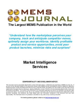
- 1. The Largest MEMS Publication in the World “Understand how the marketplace perceives your company, track and anticipate competitor moves, optimally assign your workforce, identify profitable product and service opportunities, avoid poor product launches, minimize risks and surprises” Market Intelligence Services CONFIDENTIALITY AND DISCLAIMER NOTICE This document and its associated attachments contain information that is confidential and proprietary to MEMS Journal, Inc. If you are not the intended recipient of this document, please notify MEMS Journal immediately by email or telephone, delete the original document, emails and attachment files from your computer system and destroy any hard copies of this document and its supplements. Be aware that any disclosure, copying, distribution, or use of this file or its accompanying attachments (if any) with any parties is prohibited. The content of this document is for information purposes only and is not intended to provide tax, legal or investment advice. You should not fully rely on any material contained in this document and should seek independent advice wherever necessary. Any decisions you make based upon any information contained in this document are your sole responsibility. The information does not constitute a solicitation of any order to buy or sell any securities. For further questions, please contact us at info@memsjournal.com.
- 2. Market Intelligence Services About MEMS Journal, Inc. MEMS Journal, Inc. was founded in 2003 and currently has 28,700+ subscribers worldwide. We are the only independent publication with an exclusive focus and comprehensive coverage on the latest developments in the MEMS industry. We are the largest MEMS publication in the world. Our Weekly Newsletter is specifically designed for MEMS professionals and reports on the top MEMS stories from 7000+ sources worldwide. We cover the most critical developments in the MEMS industry to ensure that our subscribers explore and take advantage of the latest client development, investment, commercialization and partnership opportunities. At this time, our subscribers include most of the leading executives, engineers and researchers in the MEMS community. Our marketing services include: Comprehensive sales and marketing program reviews Brand identity and positioning Brand awareness surveys and evaluations Market research reports Direct industry introductions and business development Partnership development Public and media relations Advertising tracking systems Social media marketing and community development Content development and “ghost writing” Dedicated email blasts Whitepaper distributions Events and workshops Webinars Advertising Sales channel development and enhancement Proprietary and Confidential Copyright 2014 MEMS Journal, Inc. Page 2 of 33
- 3. Market Intelligence Services Market Intelligence Facts and Considerations MEMS Journal has been in business since 2003 and has conducted marketing and market intelligence campaigns for 145+ companies and organizations worldwide. The following are our observations about the current state of how companies and organizations in the MEMS, microsystems, sensors and semiconductor industries approach market intelligence: ~75% of all companies and organizations do not have an active and ongoing market intelligence effort in place ~85% do not have a clear understanding of their competition’s main weaknesses ~70% of all sales people do not understand the real reasons why they have lost a potential sale ~65% of all marketing programs and budgets are wasted because the language is not optimized based on a clear understanding of the customers’ true needs and priorities ~90% of all products are developed and launched without sufficient information about the customer base and competitive offerings Proprietary and Confidential Copyright 2014 MEMS Journal, Inc. Page 3 of 33
- 4. Market Intelligence Services Top Seven Business Benefits Market Intelligence When you clearly understand your company’s optimal position marketplace, you reap a range of business benefits, including the following: 1) Higher profits: When you better understand which parts of your products and services your customers value most, you can focus on these items and improve your profitability. Also, by performing marketing intelligence studies and surveys before developing and launching new products, you will be able to dramatically reduce your R&D expenses and avoid costly marketing campaigns. 2) Premium pricing: Don’t compete on price, compete on value. When you truly understand your customers’ needs and priorities, you will be able to justify the higher price of your products and services. 3) Lower cost of sales: If clearly understand your potential clients’ needs and priorities, your sales team will be able to steer the conversation the right direction and dramatically accelerate the sales cycle. 4) Lower cost of promotion: Based on your clear understanding of the customers and competitive offering, you will be able to adjust your marketing messaging accordingly and engage your customers more effectively. This will increase the cost-effectiveness of your investments into marketing programs. 5) Higher market share: By continually and consistently, surveying your customers, prospects, competitors, as well as current and potential partners, you will be able to maintain an edge in the marketplace. With time, your market share will increase and you will take more business away from your competitors. 6) Premium pricing and reputation: Well-established brands acquire loyal customers who recruit more customers to the brand, increasing the brand’s share of market while reducing customer-development costs and building immunity to competitive attacks. 7) Lower recruiting costs: Great brands attract passionate employees, who pass their enthusiasm to satisfied consumers, who in turn make employees’ jobs more enjoyable, reducing employee turnover as a result. Your recruiting costs will also be lower and you will be able to attract higher quality talent to your organization. Proprietary and Confidential Copyright 2014 MEMS Journal, Inc. Page 4 of 33
- 5. Market Intelligence Services Market Intelligence Service Plans Level Annual Program - Package Features Diamond - $85,000 • comprehensive review of your current market intelligence program • report and recommendations to improve your market intelligence operations • ongoing strategic marketing advice and recommendations • ongoing monitoring of your competitors (quarterly reports) • ongoing monitoring of your product marketplace (quarterly reports) • thirty (30) interviews with your potential customers • ten (10) interviews with your potential partners • three (3) market research surveys on your behalf with our 28,700+ subscribers (typically yields 80-300 replies per each survey) Platinum - $55,000 • comprehensive review of your current market intelligence program • report and recommendations to improve your market intelligence operations • ongoing monitoring of your competitors (quarterly reports) • ongoing monitoring of your product marketplace (quarterly reports) • twenty (20) interviews with your potential customers • five (5) interviews with your potential partners • two (2) market research surveys on your behalf with our 28,700+ subscribers (typically yields 80-300 replies per each survey) Gold - $35,000 • comprehensive review of your current market intelligence program • report and recommendations to improve your market intelligence operations • ongoing monitoring of your competitors (quarterly reports) • ongoing monitoring of your product marketplace (quarterly reports) • fifteen (15) interviews with your potential customers • one (1) market research survey on your behalf with our 28,700+ subscribers (typically yields 80-300 replies per each survey) Silver - $15,000 • ten (10) interviews with your potential customers • one (1) market research survey on your behalf with our 28,700+ subscribers (typically yields 80-300 replies per each survey) Proprietary and Confidential Copyright 2014 MEMS Journal, Inc. Page 5 of 33
- 6. Market Intelligence Services Other Market Research Services Custom market research based on your area of interest and focus Identification of profitable product and service opportunities through our extensive industry network of 5,250+ professionals Scouting for emerging trends and applications at industry events and tradeshows – MEMS Journal is directly involved in 40-45 industry events every year Focus groups, seminars and road shows Identification of new product and service opportunities through a direct network of well established industry contacts IP and technology due diligence including introductions and access to many highly specialized experts Introductions of potential acquirers or licensors of your IP and patents Continual monitoring of specific market segments and technologies SWOT (Strengths, Weaknesses, Opportunities, and Threats) analysis Periodic market specific intelligence reports to keep track of competitors and identify business development opportunities Proprietary and Confidential Copyright 2014 MEMS Journal, Inc. Page 6 of 33
- 7. Market Intelligence Services Feedback on MEMS Journal "MEMS Journal did a great job with marketing NanoGetters and MEMS foundry services. First, they assessed our current market positioning and existing marketing practices. From there, they developed for us a comprehensive report and strategic marketing plan. They also helped us put on a webinar in April of 2011. The event attracted nearly 300 participants, many from leading MEMS companies. We look forward to continuing to work with MEMS Journal and we recommend their services highly to other MEMS companies." Doug Sparks, President and Founder, NanoGetters ***************************************************** “MEMS Journal is an extremely valuable marketing partner for us. We began working with them about a year ago on a pilot project and have quickly expanded the program from there. They have been able to deliver a steady stream of new business leads to us. If you want to expand your business and visibility in the MEMS sector, you should work with MEMS Journal. They have excellent reach and produce solid results. We recommend MEMS Journal's marketing services highly to companies with both new or established MEMS products and services.” Izabela Mijic-Yovan, Marketing Coordinator, Polytec ***************************************************** "We began to work on marketing projects with MEMS Journal in January of 2011 and our experience has been great so far. Our company is a provider of MEMS design software and services, and we need to continually connect with new potential customers who may benefit by using our products. One of the MEMS Journal initiatives that worked well for us was a webinar that focused on some of the MEMS design considerations that our current and potential customers typically face. Through the webinar, we were able to connect with hundreds of potential customers and this has already led to some new business for our company. MEMS Journal assisted us with webinar topic selection, materials preparation, webinar promotion as well as all of the associated logistics. Based on our experience, we'd highly recommend MEMS Journal's marketing services to other MEMS companies." Joe Johnson, Business Development Manager, IntelliSense ***************************************************** “MEMS Journal's technical and business knowledge and connections in the MEMS space make them an excellent resource for anyone wishing to take advantage of the opportunities in this market. They provide excellent value and high quality, with creativity and flexibility in providing an optimal mix of services. Their team is thorough and responsive – a great partner to have on your team.” Dan Hamon, Vice President and General Manager, Tanner EDA ***************************************************** "MEMS Journal has been a great marketing partner for ClassOne Equipment. We've been working with M J since 2009 and they have delivered lots of good visibility for us including new business leads. We are the leading supplier of refurbished equipment from Suss, EVG, Semitool STS, Hitachi, and KLA-Tencor. These tools fall right into MEMS wafer fabrication and inspection processes, so expanding our visibility with MEMS research institutes, startup companies, and fabs is a natural fit for ClassOne. We plan to continue working with MEMS Journal! We recommend MJ's services to other companies that want to boost their brand and advertising into MEMS and related market sectors." Byron Exarcos, President, ClassOne Equipment Proprietary and Confidential Copyright 2014 MEMS Journal, Inc. Page 7 of 33
- 8. Market Intelligence Services Feedback on MEMS Journal (continued) "As an international software provider, we have thousands of customers worldwide and utilize many marketing channels to connect with our current and potential customers. We use specific metrics to precisely measure performance of all of our marketing and advertising channels. As such, we have been working with MEMS Journal since 2007 and they have consistently proven themselves to be one of our key marketing channels. Specifically for the MEMS and microsystems market, MEMS Journal has been outstanding. W e've gradually expanded our marketing programs with them and a number of MJ's services such as email advertising, webinars and whitepaper distributions proved to be highly effective for us. MEMS Journal's team is dedicated, focused and responsive to our needs and we'd recommend them and their services to other companies who are looking to expand their presence in the MEMS and microsystems market." Bernt Nilsson, Sr. Vice President of Marketing, COMSOL ***************************************************** "MEMS Journal has been solid, reliable, energetic, and productive partner for Tegal Corporation's marketing efforts ever since we first began working together, starting in 2006. We've increasingly upped the ante with MEMS Journal along the way as a result of their proving time and again the value he brings to Tegal's marketing programs. Someone (a Sales VP) once told me the only reason marketing programs exist is to bring in sales leads, and by that measure MEMS Journal has delivered in spades. We have seen scores of new customer leads come in as a result of the webinars MEMS Journal led for us, and as a result of online advertising and conference sponsorships with the MEMS Journal (which also publishes a weekly "must read" newsletter much-admired in the MEMS community). Above all, their team’s enthusiasm for projects is contagious, they get the job done, and they are meticulous about the follow-up, which is why I will continue working with MEMS Journal and why I so highly recommend MEMS Journal's services." Paul Werbaneth, VP Marketing and Applications, Tegal Corporation ***************************************************** "I've been working with MEMS Journal since 2005 on various marketing and business development projects for many companies. I am a strong advocate of the MEMS Journal and the benefits that their company provides. Their service is great and the value they provide are extremely helpful. In my experience, the MEMS Journal offers one of the highest returns on investment for marketing programs in the MEMS Industry." David Harris, Director of Business Development, Advanced MicroSensors Corporation ***************************************************** “As a leading MEMS foundry, Innovative Micro Technology needs a marketing partner that has a comprehensive set of offerings that meet our continually evolving requirements and priorities. Over the past 4-5 years, MEMS Journal and Mike Pinelis have fulfilled this role wonderfully, and we envision a long-term, mutually beneficial relationship with them. Through our marketing programs with MEMS Journal, we get steady stream of new leads and relationships, speaking engagements at MEMS events, media and public relations counsel, and insightful market research. IMT considers MEMS Journal to be an integral marketing resource, and should be for any company in the MEMS community.” Ted Chi, Director of Marketing and Sales, Innovative Micro Technology Proprietary and Confidential Copyright 2014 MEMS Journal, Inc. Page 8 of 33
- 9. Market Intelligence Services Selected List of MEMS Journal’s Customers EV Group IMT QSecure MIG OAI DWFritz Coventor COMSOL SAES MANCEF Baolab NSTI HSystems MEMSTech AKN MEPTEC FLX Micro SUSS Micralyne SiTime BMC Springer Bosch Tyndall Vectron DALSA Miradia Siimpel Akustica Analog Devices 245+ clients in the past 10 years… Proprietary and Confidential Copyright 2014 MEMS Journal, Inc. Page 9 of 33
- 10. Market Intelligence Services Market Survey Results (sample) The following pages provide high level data from a market research and intelligence survey that MEMS Journal has conducted for one of our customers. Please note that while individual email addresses, phone numbers, and other detailed data have been removed from this document, the customer received a complete report that was ~200 pages long. The survey provided the following benefits to the customer: Comprehensive feedback from MEMS Journal’s 27,800+ MEMS focused subscribers. We are the largest MEMS publication worldwide. Continual supply of market research and intelligence data. Throughout this campaign, we generated ~120 pages of direct feedback from the customer’s potential clients who have outlined their needs and priorities (specifically, as these related to the customer’s core product and service offerings). The customer was then able to use this data to update and adjust their marketing and product development efforts. In addition to market intelligence, generation of fresh business leads to the customer and their sales and marketing team. In this case, the customer received 151 new business leads in the span of four (4) months. The customer and their distributors received pre-screened leads that came to them on a continual basis throughout this program. Savings of time. Instead of going to more tradeshows and conferences (which would have cost the customer more time and money), this program resulted in lots of new market intelligence and business leads coming directly to the customer. In this specific example, the campaign was primarily focused on North America. Proprietary and Confidential Copyright 2014 MEMS Journal, Inc. Page 10 of 33
- 11. Market Intelligence Services Type of Organization or Company R&D 26%, General Areas 26%, Manufacturing 18%, Academia 15%, Services 12%, Misc. 3% R&D General Areas Manufacturing Academia Services Misc. Proprietary and Confidential Copyright 2014 MEMS Journal, Inc. Page 11 of 33
- 12. Market Intelligence Services Geographical Distribution: Summary Continental Distribution Location of Respondents Number of Respondents (Out of Total 151) North America 94 Europe 37 Asia 11 Rest of World 9 Continental Distribution 100 90 80 70 60 50 40 30 20 10 0 Number of Respondents (Out of Total 151) North America Proprietary and Confidential Europe Asia Rest of World Copyright 2014 MEMS Journal, Inc. Page 12 of 33
- 13. Market Intelligence Services North America Distribution Location of Respondents Number of Respondents (Out of Total 94) Alberta 2 Ontario 1 Quebec 3 Mexico 2 Arizona 2 California 32 Colorado 1 Delaware 1 Florida 2 Georgia 5 Idaho 1 Indiana 1 Kentucky 1 Maryland 1 Massachusetts 8 Michigan 1 Minnesota 1 Nevada 1 New Jersey 2 New Mexico 2 New York 3 Ohio 1 Oregon 1 Pennsylvania 3 South Carolina 1 Texas 12 Utah 2 Washington 1 Proprietary and Confidential Copyright 2014 MEMS Journal, Inc. Page 13 of 33
- 14. Proprietary and Confidential Copyright 2014 MEMS Journal, Inc. Washington Utah Texas South Carolina Pennsylvania Oregon Ohio New York New Mexico New Jersey Nevada Minnesota Michigan Massachusetts Maryland Kentucky Indiana Idaho Georgia Florida Delaware Colorado California Arizona Mexico Quebec Ontario Alberta Market Intelligence Services North America Distribution (continued) North America Distribution 35 30 25 20 15 10 5 0 Page 14 of 33
- 15. Market Intelligence Services Europe Distribution Location of Respondents Number of Respondents (Out of Total 37) Austria 1 France 7 Germany 12 Greece 1 Ireland 1 Italy 2 Netherlands 2 Scotland 1 Spain 2 Switzerland 4 UK 4 Europe Distribution 14 12 10 8 6 4 Number of Respondents (Out of Total 37) 2 0 Proprietary and Confidential Copyright 2014 MEMS Journal, Inc. Page 15 of 33
- 16. Market Intelligence Services Asia Distribution Location of Respondents Number of Respondents (Out of Total 11) China 7 South Korea 3 Taiwan 1 Asia Distribution 8 7 6 5 4 Number of Respondents (Out of Total 11) 3 2 1 0 China Proprietary and Confidential South Korea Taiwan Copyright 2014 MEMS Journal, Inc. Page 16 of 33
- 17. Market Intelligence Services Rest of World Distribution Location of Respondents Number of Respondents (Out of Total 9) India 4 Israel 3 Singapore 2 Rest of World Distribution 4.5 4 3.5 3 2.5 Number of Respondents (Out of Total 9) 2 1.5 1 0.5 0 India Proprietary and Confidential Israel Singapore Copyright 2014 MEMS Journal, Inc. Page 17 of 33
- 18. Market Intelligence Services Geographical Distribution: North America Title/Position Organization Country State MNTF Coordinator University of Alberta Canada AB Managing Partner Strifler & Assocoates Canada AB President Williston Consulting Canada ON Sales manager Teledyne DALSA Canada PQ account Mgr Canada QC Canada QC Advisor Teledyne DALSA Teledyne DALSA Semiconductor Instituto Politecnico Nacional Mexico DF researcher INAOE Mexico PU MEMS Freescale USA AZ Manager, MEMS Development USA AZ Mgr, Advanced Technology Freescale R&D - BridgeWave Comm. USA CA VP Design Engineering Microfabrica USA CA Consultant GC Consulting USA CA research staff Bruker USA CA mgr wd USA CA mechanical engineer bio-rad lab USA CA Account Technology Director USA CA USA CA USA CA C.E.O. Intermolecular Silicon Microstructures Inc Philips Lumileds Lighting Co. Yield Engineering Systems USA CA Technology Director AMEC USA CA Director Pacrim Tech USA CA Engineer MEMS, Business Development Manager Oracle USA CA Micrel,Inc. A.M.Fitzgerald & Associates USA CA USA CA USA CA MEMS Des&Dev Mgr Senior Member of Research Staff Intermolecular Meggitt Sensing Systems Palo Alto Research Center USA CA USA CA Product Manager STATSChipPAC USA CA PCB Technology Apple USA CA VP Business development Invenios USA CA Engineer Cisco USA CA MEMS Integration Engineer MEMS Design Manager Sr. Staff Development Engineer Engineer Director, Account Technology Proprietary and Confidential Copyright 2014 MEMS Journal, Inc. Page 18 of 33
- 19. Market Intelligence Services Research Assistant UC Irvine USA CA Director, MEMS Fabrication USA CA Staff Engineer Invensense Inc. Fairchild Semiconductor USA CA Director Genapsys USA CA Mgr, Advanced Packaging Cisco USA CA Director of Operations InvenSense USA CA Director of R&D SMI USA CA sr. acct. mgr. Lead Package Design Engineer classone equipment USA CA GE USA CA Corporate Engineer mCube Advanced Microsystems USA CA USA CO USA DE CEO AL Intelligent Micro Patterning LLC USA FL Eng Plasma ther USA FL Graduate student Georgia Tech USA GA Student Georgia Tech USA GA GRA Georgia tech USA GA PhD Student Georgia Tech USA GA PHD Candidate Georgia Tech USA GA President DFX Solutions, Inc. USA ID Research Engineer Purdue University USA IN Dir Operations CeNSE University of Kentucky USA KY engineer nasa USA MD MEMS eng mgr Symmetricm USA MA Staff Scientist Manager of Applications Engineering Harvard University USA MA Coventor Inc. USA MA Technical Staff MSSA, Inc USA MA engineering manager fab engineering USA MA Reearch Scientist MIT USA MA VP of Operations Qualtre USA MA Student MIT USA MA EVP Hanking USA MI Engineer Seagate Technology USA MN VP, Research Gartner USA NV Director R&D Johnson & Johnson Kulite Semiconductor Products USA NJ USA NJ Cornell University MCB Clean Room Solutions, LLC USA NY USA NY President Research Staff Development Engineer Research Staff CTO Proprietary and Confidential Copyright 2014 MEMS Journal, Inc. Page 19 of 33
- 20. Market Intelligence Services Senior Scientist Cornell NanoScale Facility Sandia National Laboratory USA NM consultant J Allen Consulting USA NM manager DNV USA OH Editor Techfocus Media USA OR VP Sales & Marketing co-Director - Nanofabrication Facility Akrion Systems USA PA Penn State USA PA physics professor Grove City College USA PA Process Engineer formulation USA SC Integration Engineer Novati USA TX Staff Engineer Novati Technologies USA TX eng samsung USA TX CTO 200mm Global Product / Marketing Manager Sachem Inc USA TX Applied Materials USA TX Working Group Manager GSA USA TX Consultant 200mm Global Product / Marketing Manager R W Gooch USA TX Applied Materials USA TX Sutduent UT Dallas USA TX President VISM Corp. USA TX Integration Engineer SVTC USA TX GRA Nanofab USA TX Assoc. Dir. Utah Nanofab USA UT RA University of Utah USA UT ceo sensors in motion USA WA Research Support Specialist Proprietary and Confidential Copyright 2014 MEMS Journal, Inc. USA NY Page 20 of 33
- 21. Market Intelligence Services Geographical Distribution: Europe Title/Position Organization Vienna University of Technology Country process engineer Head of Sensors & Microtehnology Unit Director Euroepan Operations and Foundry Program ESIEE paris ONERA - The French Aerospace Lab France Coventor France Mems design Engineer France Research department head Schlumberger Mems-Tc Institut d'Electronique Fondamentale Engineer LAAS-CNRS France engineer FEMTO-ST, CNRS France Director Germany Project Manager EPCOS AG (part of TDK) endress+Hauser GmbH+Co.KG Engineer IHP Germany Project Manager CiS Forschungsinstitut Germany Senior Scientist Fraunhofer IZM Germany R&D Manager FhG IPMS Germany Process Specialist Etch IFW Dresden Germany Researcher Germany Dipl.-Ing. TU Chemnitz Ilmenau University of Technology, IMN MacroNano Researcher University of Ulm Germany Research Engineer Germany Univ. Prof. Fraunhofer IZM Westf. WilhelmsUniversität Münster, Germany Physicist researcher NCSR Demokritos Greece consultant Ashgrove consulting Ireland Manager STM Italy technologist kessler Foundation Italy - Oce Netherlands Senior Scientist TNO Netherlands Research Fellow University of Edinburgh Scotland Professor IMB-CNM, CSIC Spain Scientific Research IMB-CNM (CSIC) Spain Technologist Karmic Sarl Switzerland Lecturer FHNW-HLS-LIMA Switzerland PhD student Proprietary and Confidential Copyright 2014 MEMS Journal, Inc. Austria France France Germany Germany Germany Page 21 of 33
- 22. Market Intelligence Services head of market r&d Endress+Hauser Switzerland . Reader in Experimental Physics Rolex SA Switzerland Cardiff University UK Researcher Univeristy of Edinburgh Applied Microengineering Ltd UK Linde Electronics UK Technical Director Manager new product Development and Commercialisation Proprietary and Confidential Copyright 2014 MEMS Journal, Inc. UK Page 22 of 33
- 23. Market Intelligence Services Geographical Distribution: Asia Title/Position Organization Country consultant Assistant Chief Engineer SAE China China Electronics Technology Group Corporation The 49th Research Institute China PH.D student Northwestern polytechnical university China PH.D Master of Science Northwetern Polytechnical University China Peking University China Professor Southeast University China professor Suzhou Inst of Nanotech China Manager R&D South Korea Researcher Dongbu HiTek South Korea CEO MEMS Solution Inc South Korea Prof. National Cheng Kung University Taiwan Proprietary and Confidential Copyright 2014 MEMS Journal, Inc. Page 23 of 33
- 24. Market Intelligence Services Geographical Distribution: Rest of World Title/Position Country SRF Organization Central Electronics Engineering Research Institute (CEERI- CSIR) lecturer jecrc India Professor Indian Institute of Technology India Assoc Professor IIT Kharagpur India Associate Professor School of Mech. Eng. Tel Aviv Univesity Israel CEO IMH Israeli MEMS House Israel VP Eng. Sr Product Marketing Manager Maradin Israel KLA-Tencor Singapore Senior Scientist Institute of Microelectronics Singapore Proprietary and Confidential Copyright 2014 MEMS Journal, Inc. India Page 24 of 33
- 25. Market Intelligence Services Interviews with Potential Customers (samples) The following pages provide samples of interviews with potential customers for a specific product or service. In this case, the focus was on through substrate vias (TSVs) and 3D packaging solutions. Also, in this case, the interviews were shorter because our client wanted to have more interviews and feedback. As such, ~40 one-page interviews were collected as part of this study. The interviews provided the following benefits to the customer: Detailed feedback from potential customers and partners. Identification of challenges and “pain points” facing customers Enhanced understanding of how potential customers currently use existing solutions Enhanced understanding of the competitive landscape For this particular study, our client wanted the interviews to be conducted via email and they also wanted to see the “raw” and unedited replies from the respondents. Proprietary and Confidential Copyright 2014 MEMS Journal, Inc. Page 25 of 33
- 26. Market Intelligence Services Interview Sample #1 Name & Title: Name Removed (sample), Assistant Manager Organization & Location: Asahi Glass Co., Ltd./Technology Development General Div., AGC Electronics -Tokyo, Japan Contact Number & Email: Phone Number and Email Address Removed (sample) Please describe in detail about what your company does and how it relates to 3D Packaging and/or TSVs. Please include the types of companies who are your main customers, as well as companies that are your main suppliers. We produce several glass materials for semiconductor packaging, as some examples, which are glass frit for hermetic sealing, carrier glass for silicon processing, and cover glass for sensor. Foundries and memory makers are our main customer in terms of carrier glass. And glass frit is used by several industries. Please describe in detail your personal involvement (vs. your company or organization in general) with 3D packaging technologies and/or processes. I’m responsible for marketing to establish new business or new products. Currently I’m focusing 3D integration for semiconductor market. Especially 3D integrated packaging using interposer is very interesting. I have also experience about chip bonding technology. Please describe in detail your personal involvement with TSV processes and/or technologies In terms of TSV, I expect our carrier glass is used for silicon thinning process. Furthermore, I’m also involved TGV (through glass via, not TSV) development. I’m looking for some application for this. For your ongoing 3D packaging and/or TSV projects, what are the main challenges (business and/or technical) that you are encountering? What’s causing most of your challenges and why. TGV technology. Fine pitch hole drilling and metallization process for this. To look for possible application for this, I’d like to connect some people from packaing industry. Are you personally a buyer or a seller of 3D packaging or TSV technologies or services? Which specific 3D packaging technologies or services do you primarily buy or sell? If you both buy and sell, please include information for both. We are material company. We sell some glass to packaging makers. Proprietary and Confidential Copyright 2014 MEMS Journal, Inc. Page 26 of 33
- 27. Market Intelligence Services Interview Sample #2 Name & Title: Name Removed (sample), Architect Organization & Location: Cadence Design Systems - Chelmsford, MA Contact Number & Email: Phone Number and Email Address Removed (sample) Please describe in detail about what your company does and how it relates to 3D Packaging and/or TSVs. Please include the types of companies who are your main customers, as well as companies that are your main suppliers. Cadence Design Systems is a EDA tool provider. Our tool set includes circuit schematic design, physical layout automation, model extraction and simulation. The tool set covers from IC, packaging and PCB. So our customer uses the tool to design their packaging, 2D or 3D and design the TSVs. Intel, IBM, and Cisco are our main customers among many others. We use many software tools from Microsoft, Intel and use computing facilities from Dell, IBM and Lenovo Please describe in detail your personal involvement (vs. your company or organization in general) with 3D packaging technologies and/or processes. I am in SPB division which stands for Silicon-Packaging-Board and working on interconnect model extraction which includes packaging interconnect characterization and is used for signal integrity analysis. Please describe in detail your personal involvement with TSV processes and/or technologies When design packaging interposer, the TSV needs to be designed together as well. Due to the material complexity and complicated electromagnetic behavior, the accurate characterization is required which requires advanced analyze methodology numerically and theoretically and which is one of my working area. For your ongoing 3D packaging and/or TSV projects, what are the main challenges (business and/or technical) that you are encountering? What’s causing most of your challenges and why. In my area, acquiring the accurate physical structure in 3D and accurate material specification are the first things. Given these information, how to accurately and effectively characterize the packaging interconnect and TSV’s electrical behavior are big challenges. Are you personally a buyer or a seller of 3D packaging or TSV technologies or services? Which specific 3D packaging technologies or services do you primarily buy or sell? If you both buy and sell, please include information for both. Basically I am using Microsoft software to design EDA software on Lenovo’s computer. Proprietary and Confidential Copyright 2014 MEMS Journal, Inc. Page 27 of 33
- 28. Market Intelligence Services Interview Sample #3 Name & Title: Name Removed (sample), Sr. Director, Technical Sourcing Organization & Location: Infinera - Sunnyvale, CA Contact Number & Email: Phone Number and Email Address Removed (sample) Please describe in detail about what your company does and how it relates to 3D Packaging and/or TSVs. Please include the types of companies who are your main customers, as well as companies that are your main suppliers. Network Transport Equipment We build optical transport systems and software that install in the Service Provider and Cable Systems networks (e.g. Level 3, Cable & Wireless, Duestche Telecom, etc.) for the networking transport of their backbone and core networks. Our systems contain ASICs that help with the switching and routing functions at high bandwidths – 1 Tb/s and above. So, we are exploring new technologies to package our complex products using multi-die solutions such as TSV and 3D packaging technologies. Please describe in detail your personal involvement (vs. your company or organization in general) with 3D packaging technologies and/or processes. Technical Sourcing – Operations We work with our Architecture & Engineering teams to source various suppliers to select and qualify high end 2.5D and 3D packaging technology solutions. Please describe in detail your personal involvement with TSV processes and/or technologies Because high speed BW is a big factor, we are currently exploring die stacking and related TSV technologies for our applications. For your ongoing 3D packaging and/or TSV projects, what are the main challenges (business and/or technical) that you are encountering? What’s causing most of your challenges and why. BW, cost, power, real estate. The biggest challenge is BW performance at low power. Our ASIC requirements need 20Gb of ext DRAM operating at 1.2-1.5Tbps -> with a power budget of 80-90W Are you personally a buyer or a seller of 3D packaging or TSV technologies or services? Which specific 3D packaging technologies or services do you primarily buy or sell? If you both buy and sell, please include information for both. Yes, I am part of the team that decides on the selecting & buying this technology solution. Proprietary and Confidential Copyright 2014 MEMS Journal, Inc. Page 28 of 33
- 29. Market Intelligence Services Interview Sample #4 Name & Title: Name Removed (sample), Principal Engineer Organization & Location: Intel Corp. - Santa Clara, CA Contact Number & Email: Phone Number and Email Address Removed (sample) Please describe in detail about what your company does and how it relates to 3D Packaging and/or TSVs. Please include the types of companies who are your main customers, as well as companies that are your main suppliers. Microprocessors and many other products across multiple market segments Please describe in detail your personal involvement (vs. your company or organization in general) with 3D packaging technologies and/or processes. Defining interface between Host (my company’s design) and Memory device (external vendor’s design). The system is in a 3D packaging. Please describe in detail your personal involvement with TSV processes and/or technologies TSV used in stacked memory For your ongoing 3D packaging and/or TSV projects, what are the main challenges (business and/or technical) that you are encountering? What’s causing most of your challenges and why. Multi-discipline co-optimization between on-chip circuit, interconnect, packaging, thermal/mechanical variables Are you personally a buyer or a seller of 3D packaging or TSV technologies or services? Which specific 3D packaging technologies or services do you primarily buy or sell? If you both buy and sell, please include information for both. No Proprietary and Confidential Copyright 2014 MEMS Journal, Inc. Page 29 of 33
- 30. Market Intelligence Services Interview Sample #5 Name & Title: Name Removed (sample), Staff Engineer 3D Packaging Technologies Organization: Invensas Corp. Contact Number & Email: Phone Number and Email Address Removed (sample) Please describe in detail what your company does and how it relates to 3D Packaging and/or TSVs. Please include the types of companies who are your main customers, as well as companies that are your main suppliers. Invensas Corp., headquartered in San Jose, California, develops, invests in, licenses and delivers innovative miniaturization technologies and products for next-generation electronic devices. The company’s micro-electronics solutions enable smaller, higher-functionality devices through chipscale and wafer-level packaging, silicon-level interconnect and 3D packaging. Samsung and Hynix are main customers. Please describe in detail your personal involvement (vs. your company or organization in general) with 3D Packaging technologies and/or processes Involved in 3D packaging technology development. Lead engineer in reliability and failure analysis on all of the 3D packaging projects. Provide support in materials design and selection, characterization. Are you personally a buyer or a seller of 3D packaging technologies or services? Which specific 3D packaging technologies or services do you primarily buy or sell? If you both buy and sell, please include information for both. Invensas is a seller of 3D packaging technologies, mostly in DRAM with multiple memory chips in a single package. Please describe in detail your personal involvement with TSV processes and/or technologies. Technology development. Reliability and failure analysis. Materials interaction analysis, characterization. Are you personally a buyer or a seller of TSV technologies or services? Which specific TSV technologies or services do you primarily buy or sell? If you both buy and sell, please include information for both. Invensas acquired the patent assets of ALLVIA, Inc. In addition, Invensas has entered into a two-year collaborative partnership with ALLVIA to further develop technology and intellectual property (IP) in the 3dimensional integrated circuit (3D-IC) packaging space. The majority of the 64 acquired patents and patent applications from ALLVIA relate to 3D-IC, including through-silicon via (TSV) technology and silicon interposer technology, which is often known as 2.5D. This IP portfolio purchase, along with our collaboration on further 3D-IC development marks another important step on Invensas’ path of continued innovation in vital next-generation packaging technologies Proprietary and Confidential Copyright 2014 MEMS Journal, Inc. Page 30 of 33
- 31. Market Intelligence Services Interview Sample #6 Name & Title: Name Removed (sample), Manager, Assembly and Packaging Designs Organization & Location: Maxim Integrated Products - Dallas, TX Contact Number & Email: Phone Number and Email Address Removed (sample) Please describe in detail about what your company does and how it relates to 3D Packaging and/or TSVs. Please include the types of companies who are your main customers, as well as companies that are your main suppliers. Analog Mix Signal IC designs for multiple markets. We design and develop product for hand held, automotive, consumer, industrial, power and energy market along with many other in communication related areas as well. Please describe in detail your personal involvement (vs. your company or organization in general) with 3D packaging technologies and/or processes. Working with the team of wafer level packaging to extend the development of the thru silicon via enabled devices to take it to the next level of integration if IPD and fanout WLP as well as conventional epoxy molded packaging. Please describe in detail your personal involvement with TSV processes and/or technologies Personally I am involved in packaging side of the TSV wafers. So process development is done and we characterize the TSV performance based on the standard packaging development and assembly process development need and its interaction with respect to packaging process, material sets and long term reliability of the TSV in a given package. For your ongoing 3D packaging and/or TSV projects, what are the main challenges (business and/or technical) that you are encountering? What’s causing most of your challenges and why. Getting right set of materials for given packaging technology using the TSV based devices. Stress inside the package specially seen at the via structure due to molding process under thermal excursions, is a major challenge. Are you personally a buyer or a seller of 3D packaging or TSV technologies or services? Which specific 3D packaging technologies or services do you primarily buy or sell? If you both buy and sell, please include information for both. Yes -- for Assembly side of it for both development as well as assembly services. Proprietary and Confidential Copyright 2014 MEMS Journal, Inc. Page 31 of 33
- 32. Market Intelligence Services Interview Sample #7 Name & Title: Name Removed (sample), Principal Engineer Organization & Location: Semiconductor Manufacturing International Corp - Shanghai, China Contact Number & Email: Phone Number and Email Address Removed (sample) Please describe in detail about what your company does and how it relates to 3D Packaging and/or TSVs. Please include the types of companies who are your main customers, as well as companies that are your main suppliers. SMIC is a leading foundry in mainland China. We provide 40nm – 0.35um tech node logic and other device fabrication services. We have a TSV project in progress now. Our customer wants us to implement TSV on their CIS devices. Please describe in detail your personal involvement (vs. your company or organization in general) with 3D packaging technologies and/or processes. Our TSV project is still in development progress. I’m the owner of plating process of TSV, with Raider-S of AMAT. Base on the customers’ requirements and current process development status, we started with 8’ wafers for TSV. So maybe there’s less relations to packaging. But almost every foundry do the same TSV development as us. Foundry likes via-middle TSV process. Please describe in detail your personal involvement with TSV processes and/or technologies Our TSV project is still in development progress. I’m the owner of plating process of TSV, with Raider-S of AMAT. For your ongoing 3D packaging and/or TSV projects, what are the main challenges (business and/or technical) that you are encountering? What’s causing most of your challenges and why. Plating is the main challenge of our project. We’re trying MSA based chemistries and the tool might also has something to improve. And, overburden after plating will be a big cost challenge to us. Are you personally a buyer or a seller of 3D packaging or TSV technologies or services? Which specific 3D packaging technologies or services do you primarily buy or sell? If you both buy and sell, please include information for both. No, I’m not involved of 3D packaging purchase or sales. Proprietary and Confidential Copyright 2014 MEMS Journal, Inc. Page 32 of 33
- 33. Market Intelligence Services Interview Sample #8 Name & Title: Name Removed (sample), Director of Business Development Organization & Location: Ziptronix - Austin, TX Contact Number & Email: Phone Number and Email Address Removed (sample) Please describe in detail about what your company does and how it relates to 3D Packaging and/or TSVs. Please include the types of companies who are your main customers, as well as companies that are your main suppliers. Ziptronix is a pioneer in the development of low-temperature direct bond technology for a variety of semiconductor applications, including backside-illuminated (BSI) sensors, RF front-ends, pico projectors, memories and 3D integrated circuits. Its patented, scalable 3D-integration technology, including ZiBondTM and DBI®, provides the lowest-cost bonding solution for 3D technology, while enabling size reduction, yield enhancement, lower production costs and power consumption, and increased system performance. The company holds more than 35 U.S. patents and more than 20 international patents in nine foreign countries and Europe. It has more than 45 U.S. and international patent applications pending. Ziptronix licenses its technology throughout the semiconductor supply chain, including OEMs, IDMs and some fabrication and assembly facilities, and operates a back-end-of-line R&D facility with 6,000 square feet (557m2) of Class 100/1000 cleanroom space at its headquarters in Research Triangle Park, N.C. Examples of potential customers are IDM’s such as Sony, TI, Samsung or IBM, although most of our customers don’t allow us to reveal their names. In addition, we work with fabless customers as well. Please describe in detail your personal involvement (vs. your company or organization in general) with 3D packaging technologies and/or processes. 3D has been my primary focus since 2007, even before I joined Ziptronix. I was the Business Development Manager with SUSS MicroTec. After that I was the Director of Business Development for Alchimer (3D company that licenses technology for high aspect ratio TSV’s). I joined Ziptronix in mid- 2010 and have been the Director for Business Development for them ever since. Please describe in detail your personal involvement with TSV processes and/or technologies For the past two and a half years, I have been working to license a technology than can work in conjunction or potentially in place of TSV’s. Ziptronix DBI ® technology connects substrates at the die or wafer level at pitches as small or smaller than 1um. Prior to that I worked to license Alchimer technology for enabling a high aspect ratio TSV (seed, barrier and isolation layers prior to electroplating). For your ongoing 3D packaging and/or TSV projects, what are the main challenges (business and/or technical) that you are encountering? What’s causing most of your challenges and why. Ongoing challenges are issues with Known Good Die or yield that sometimes limit customers abilities to make the integration at the wafer level rather than the die level. Are you personally a buyer or a seller of 3D packaging or TSV technologies or services? Which specific 3D packaging technologies or services do you primarily buy or sell? If you both buy and sell, please include information for both. I primarily sell 3D technology licenses and some manufacturing services. Proprietary and Confidential Copyright 2014 MEMS Journal, Inc. Page 33 of 33