SlideShare ist ein Scribd-Unternehmen logo
1 von 141
Downloaden Sie, um offline zu lesen
Transparent & Flexible Electronics
Massimo Marrazzo - biodomotica.com 1
Nanotechnology
VOL. I
2011
Transparent & flexible electronics
MASSIMO MARRAZZO - BIODOMOTICA®
Transparent & Flexible Electronics
2 Massimo Marrazzo - biodomotica.com
IIIIIIIInnnnnnnnddddddddeeeeeeeexxxxxxxx
Nanotechnology pag.3
Graphene 7
Nanotubes 8
Printed electronics 13
Ink for "printed electronics" 19
Printer for "printed electronics" 21
Transparent and Strong Plastic 24
Transparent Electronics 25
Flexible and trasparent displays 30
Electronic paper / E-paper / E-ink 32
Printed battery 33
Charging batteries without wires 45
WiTricity 46
Solar Energy 48
Seebeck effect - Thermoelectric 55
Printed Memory 77
Printed Antennas 79
Wireless technologies 81
Nanotube Radio 84
Sound 87
Lens 94
Bio-Sensors 98
Virtual Muscles 101
Gecko 106
Mems 113
Ecology 115
Link to transparent electronics 116
Applications of transparent or flexible electronics 117
Invisibility Cloak 125
Acronyms 128
Books 130
Journal Papers 133
Links 134
Show/Convention/Exposition 136
Blogs 136
Toolbox 137
iPad & iPhone applications for Nanotech 138
Android applications for read RSS Nanotech 139
2011 Update 140
Transparent & Flexible Electronics
Massimo Marrazzo - biodomotica.com 3
NNNNNNNNaaaaaaaannnnnnnnooooooootttttttteeeeeeeecccccccchhhhhhhhnnnnnnnnoooooooollllllllooooooooggggggggyyyyyyyy
- http://www.nano.org.uk/whatis.htm
What is Nanotechnology?
Nanotechnology originates from the Greek word “nanos” meaning “dwarf".
A nanometre is one billionth (10-9) of a metre, which is tiny, only the length of ten hydrogen atoms,
or about one hundred thousandth of the width of a hair! Although scientists have manipulated
matter at the nanoscale for centuries, calling it physics or chemistry, it was not until a new
generation of microscopes were invented in the nineteen eighties in IBM, Switzerland that the
world of atoms and molecules could be visualized and managed.
In simple terms, nanotechnology can be defined as 'engineering at a very small scale', and this
term can be applied to many areas of research and development: from medicine to manufacturing
to computing, and even to textiles and cosmetics. It can be difficult to imagine exactly how this
greater understanding of the world of atoms and molecules has and will affect the everyday objects
we see around us, but some of the areas where nanotechnologies are set to make a difference are
described below.
From Micro to Nano
Nanotechnology, in one sense, is the natural continuation of the miniaturization revolution that we
have witnessed over the last decade, where millionth of a metre (10-6 m) tolerances
(microengineering) became commonplace, for example, in the automotive and aerospace
industries enabling the construction of higher quality and safer vehicles and planes. It was the
computer industry that kept on pushing the limits of miniaturization, and many electronic devices
we see today have nano features that owe their origins to the computer industry — such as
cameras, CD and DVD players, car airbag pressure sensors and inkjet printers.
©2008 Institute of Nanotechnology
- http://www.crnano.org/whatis.htm
What is Nanotechnology?
A basic definition: Nanotechnology is the engineering of functional systems at the molecular scale.
This covers both current work and concepts that are more advanced.
In its original sense, 'nanotechnology' refers to the projected ability to construct items from the
bottom up, using techniques and tools being developed today to make complete, high performance
products.
The Meaning of Nanotechnology
When K. Eric Drexler popularized the word 'nanotechnology' in the 1980's, he was talking about
building machines on the scale of molecules, a few nanometers wide motors, robot arms, and even
whole computers, far smaller than a cell. Drexler spent the next ten years describing and analyzing
these incredible devices, and responding to accusations of science fiction. Meanwhile, mundane
technology was developing the ability to build simple structures on a molecular scale. As
nanotechnology became an accepted concept, the meaning of the word shifted to encompass the
simpler kinds of nanometer-scale technology. The U.S. National Nanotechnology Initiative was
created to fund this kind of nanotech: their definition includes anything smaller than 100
nanometers with novel properties.
Transparent & Flexible Electronics
4 Massimo Marrazzo - biodomotica.com
Four Generations
Mihail (Mike) Roco of the U.S. National Nanotechnology Initiative has described four generations of
nanotechnology development (see chart below). The current era, as Roco depicts it, is that of
passive nanostructures, materials designed to perform one task. The second phase, which we are
just entering, introduces active nanostructures for multitasking; for example, actuators, drug
delivery devices, and sensors. The third generation is expected to begin emerging around 2010
and will feature nanosystems with thousands of interacting components. A few years after that, the
first integrated nanosystems, functioning (according to Roco) much like a mammalian cell with
hierarchical systems within systems, are expected to be developed.
© 2002-2008 Center for Responsible Nanotechnology TM CRN is an affiliate of World Care®, an international, non-profit,
501(c)(3) organization.
Transparent & Flexible Electronics
Massimo Marrazzo - biodomotica.com 5
- http://en.wikipedia.org/wiki/Nano-
Nano- (symbol n) is a prefix in the metric system denoting a factor of 10−9 or 0.000000001. It is frequently
encountered in science and electronics for prefixing units of time and length, such as 30 nanoseconds
(symbol ns), 100 nanometres (nm) or in the case of electrical capacitance, 100 nanofarads (nF).
The prefix is derived from the Greek νάνος, meaning "dwarf", and was officially confirmed as standard in
1960.
In the United States, the use of the nano prefix for the farad unit of electrical capacitance is uncommon;
capacitors of that size are more often expressed in terms of a small fraction of a microfarad or a large
number of picofarads.
When used as a prefix for something other than a unit of measure, as in "nanoscience", nano means relating
to nanotechnology, or on a scale of nanometres. See nanoscopic scale.
SI prefixes
Prefix Symbol 10n Decimal Short scale Long scale
yotta Y 1024 1000000000000000000000000 Septillion Quadrillion
zetta Z 1021 1000000000000000000000 Sextillion Trilliard
exa E 1018 1000000000000000000 Quintillion Trillion
peta P 1015 1000000000000000 Quadrillion Billiard
tera T 1012 1000000000000 Trillion Billion
giga G 109 1000000000 Billion Milliard
mega M 106 1000000 Million
kilo k 103 1000 Thousand
hecto h 102 100 Hundred
deca da 101 10 Ten
10
0
1 One
deci d 10-1 0.1 Tenth
centi c 10-2 0.01 Hundredth
milli m 10-3 0.001 Thousandth
micro ì 10-6 0.000001 Millionth
nano n 10-9 0.000000001 Billionth Milliardth
pico p 10-12 0.000000000001 Trillionth Billionth
femto f 10-15 0.000000000000001 Quadrillionth Billiardth
atto a 10-18 0.000000000000000001 Quintillionth Trillionth
zepto z 10-21 0.000000000000000000001 Sextillionth Trilliardth
yocto y 10-24 0.000000000000000000000001 Septillionth Quadrillionth
The International System of Units (SI) specifies a set of unit prefixes known as SI prefixes or metric prefixes.
An SI prefix is a name that precedes a basic unit of measure to indicate a decadic multiple or fraction of the
unit. Each prefix has a unique symbol that is prepended to the unit symbol.
Name Abbrev. Decimal Representative objects with this size scale
metre m 100 Height of a 7-year-old child.
deci- dm 10-1 Size of our palm.
centi- cm 10-2 Length of a bee.
milli- mm 10-3 Thickness of ordinary paperclip.
micro- ìm 10-6 Size of typical dust particles.
nano- nm 10-9 The diametre of a C60 molecule is about 1 nm.
pico- pm 10-12 Radius of a Hydrogen Atom is about 23 pm.
femto- fm 10-15 Size of a typical nucleus of an atom is 10 fm.
atto- am 10-18 Estimated size of an electron
Transparent & Flexible Electronics
6 Massimo Marrazzo - biodomotica.com
http://commons.wikimedia.org/wiki/Commons:Featured_picture_candidates/Image:Biological_and_technological_scales_compared-en.svg
Transparent & Flexible Electronics
Massimo Marrazzo - biodomotica.com 7
GGGGGGGGrrrrrrrraaaaaaaapppppppphhhhhhhheeeeeeeennnnnnnneeeeeeee
- http://en.wikipedia.org/wiki/Graphene
Graphene is a one-atom-thick planar sheet of sp2-bonded carbon atoms that are densely packed
in a honeycomb crystal lattice. It can be viewed as an atomic-scale chicken wire made of carbon
atoms and their bonds. The name comes from GRAPHITE + ENE; graphite itself consists of many
graphene sheets stacked together.
Graphene is an atomic-scale chicken wire
made of carbon atoms.
Integrated circuits
Graphene has the ideal properties to be an excellent component of integrated circuits. Graphene has a high
carrier mobility, as well as low noise allowing it to be utilized as the channel in a FET. The issue is that single
sheets of graphene are hard to produce, and even harder to make on top of an appropriate substrate.
Researchers are looking into methods of transferring single graphene sheets from their source of origin
(mechanical exfoliation on SiO2 / Si or thermal graphitization of a SiC surface) onto a target substrate of
interest. In 2008, the smallest transistor so far, one atom thick, 10 atoms wide was made of graphene.
Transparent conducting electrodes
Graphene's high electrical conductivity and high optical transparency make it a candidate for transparent
conducting electrodes, required for such applications as touchscreens, liquid crystal displays, organic
photovoltaic cells, and OLEDs. In particular, graphene's mechanical strength and flexibility are advantageous
compared to indium tin oxide, which is brittle, and graphene films may be deposited from solution over large
areas.
Transparent & Flexible Electronics
8 Massimo Marrazzo - biodomotica.com
NNNNNNNNaaaaaaaannnnnnnnoooooooottttttttuuuuuuuubbbbbbbbeeeeeeeessssssss
- http://en.wikipedia.org/wiki/Carbon_nanotube
3D model of three types of single-walled carbon nanotubes.
Carbon nanotubes (CNTs) are allotropes of carbon with a nanostructure that can have a length-to-diameter
ratio greater than 1,000,000. These cylindrical carbon molecules have novel properties that make them
potentially useful in many applications in nanotechnology, electronics, optics and other fields of materials
science. They exhibit extraordinary strength and unique electrical properties, and are efficient conductors of
heat. Inorganic nanotubes have also been synthesized.
Their name is derived from their size, since the diameter of a nanotube is in the order of a few nanometers
(approximately 1/50,000th of the width of a human hair), while they can be up to several millimeters in length
(as of 2008). Nanotubes are categorized as single-walled nanotubes (SWNTs) and multi-walled nanotubes
(MWNTs).
- http://www.unidym.com/technology/about_carbon.html
What are Carbon Nanotubes?
Carbon nanotubes (CNTs) are tubular cylinders of carbon atoms that have extraordinary electrical,
mechanical, optical, thermal, and chemical properties.
Transparent & Flexible Electronics
Massimo Marrazzo - biodomotica.com 9
Individual carbon nanotubes can conduct electricity better than copper, possess higher tensile strength than
steel, and conduct heat better than diamond. In electronic applications, carbon nanotubes can possess higher
mobilities than single crystal silicon. All this in a material that is over 10,000 times thinner than a human hair.
There are multiple forms of carbon nanotubes, varying in diameter, length, and in the tendency of the
nanotubes to form ropes and bundles of tubes. Some forms of carbon nanotubes are metallic and highly
conducting; other forms are semiconducting, and can form the basis of electronic switches.
- http://www.unidym.com/technology/about_carbon_more.html
CARBON NANOTUBES
Carbon nanotubes (fullerene nanotubes) are part of the fullerene family of carbon materials discovered by Dr.
Richard E. Smalley and colleagues in 1985. They include single-wall carbon nanotubes (SWNTs), and nested
(endohedral or endotopic) SWNTs, i.e., one, two or more tubular fullerenes nested inside another tubular
fullerene. Each tubular fullerene is a huge carbon molecule, often having millions of carbon atoms bonded
together to form a tiny tube. Carbon nanotube diameters range from about 0.5 to about 10 nanometers (one
nanometer = 10-9 meter) and their lengths are typically between a few nanometers and tens of microns (one
micron = 10-6 meter).
Carbon is a truly remarkable atom. It readily bonds with itself into extended sheets of atoms comprising linked
hexagonal rings shown below. Each carbon atom is covalently bonded to its three nearest neighbors.
Transparent & Flexible Electronics
10 Massimo Marrazzo - biodomotica.com
This unique sheet structure is called graphene. Solid graphite is made up of layers of graphene stacked as
shown above. No other element in the periodic table bonds to itself in an extended network with the strength of
the carbon-carbon bond, which is among the strongest of chemical bonds. Some of the electrons in the
carbon-carbon bonds are free to move about the entire graphene sheet, rather than stay home with their donor
atoms, giving the structure good electrical conductivity. The tight coupling between atoms in the carbon-
carbon bond provides an intrinsic thermal conductivity that exceeds almost all other materials. As suggested
by the carbon nanotube figure above, the structure of a fullerene nanotube is that of a sheet of graphene,
wrapped into a tube and bonded seamlessly to itself. This is a true molecule with every atom in its place and
very few defects: an example of molecular perfection on a relatively large scale.
The special nature of the bonded carbon sheet, the molecular perfection of carbon nanotubes, and their long
tubular shape endow them with physical and chemical properties that are unlike those of any other material.
These properties include high surface area, excellent electrical and thermal conductivity, and tremendous
tensile strength, stiffness, and toughness.
In a single tube, every atom is on two surfaces - the inside and the outside, and a single gram of nanotubes
has over 2400 m2 of surface area! The nature of the carbon bonding gives the tubes their great tensile
strength and electrical and thermal conductivity. The carbon nanotubes' stiffness and toughness derives from
their molecular perfection. In most materials the actual observed stiffness and toughness are degraded very
substantially by the occurrence of defects in their structure. For example, high strength steel typically fails at
about 1% of its theoretical breaking strength. Carbon nanotubes, however, achieve values very close to their
theoretical limits because of their perfection of structure - there are no structural defects where mechanical
failures can begin! It is, however, the tubular geometry of carbon nanotubes that gives them their most exotic
properties. Depending on the orientation of the graphene sheet forming the tube's wall, the tube can be either
metallic or semiconducting. The metallic tubes conduct electricity just as metals do and the semiconducting
ones have great promise as the basic elements of a new paradigm for electronic circuitry at the molecular
level.
Basic Structure
There are literally hundreds of different carbon nanotube structures. One can identify these structures by
thinking of the carbon nanotube as a sheet of graphene wrapped into a seamless cylinder. As one might
imagine, there are many ways to wrap a graphene cylinder, and the cylinder can have a wide range of
dimensions. Soon after fullerene nanotubes were discovered, a classification scheme was devised to describe
the different conformations of graphene cylinders. This classification scheme uses an ordered pair of numbers,
(n,m), and is based upon the diagram of graphene shown below. Each carbon atom in the graphene sheet is
bonded to three other carbon atoms, forming a Y-shaped vertex of carbon-carbon bonds. In order to make a
seamless graphene tube of a uniform diameter, one must wrap the graphene sheet in a way that permits every
carbon atom in the cylinder to be bonded to three other carbon atoms where the sheet joins to itself. The
number of ways this wrapping can be achieved is countable according to the numbering scheme given in the
figure below. The unit vectors of the 2-dimensional graphene lattice are shown as a1 and a2 below. Each
vertex that could possibly join to the origin during a wrapping operation is labeled with an ordered pair wherein
the first number of the pair is the distance (in lattice repeat units) of the vertex from the origin along a1, and
the second number is the distance of the vertex from the origin along a2.
Transparent & Flexible Electronics
Massimo Marrazzo - biodomotica.com 11
- http://www.unidym.com/technology/cnt_application_electronics.html
Transparent Conductive Films
One of the more amazing attributes of carbon nanotubes is that they can form films that are highly electrically
conductive, but almost completely transparent. The film is only about 50 nanometers thick, and very porous.
Under an electron microscope, the film is seen to be a just a few layers of endless carbon nanotube ropes.
The films have an ideal conductivity for multiple types of touch screens which have applications including
point-of-sale terminals, games, portable computers, cell phones, personal digital assistants and many others.
The transparent films used initially for touch screens also reach any application that requires a large-area
transparent conductor, including LCD displays, plastic solar cells, and organic LED lighting, and transparent
carbon nanotube films have been demonstrated in the laboratory to be effective in all these areas.
Printable Transistors
The semiconducting properties of carbon nanotubes can be exploited to create printable transistors with
extremely high performance. Specifically, researchers have shown CNT-based transistors employing a sparse
nanotube network to achieve mobilities of 1 cm2/V-s (Schindler et al., Physica E (2006), while those using an
aligned array of single-walled nanotubes can reach as high as 480 cm2/V-s [Kang et al., Nature Nanotech. 2,
230 (2007)]. Nanotubes also prove to be useful additives to polymer-based TFTs and help to overcome some
of the shortcomings of those devices. Beyond their performance, such devices are compatible with solution-
based printing techniques, which enable dramatic cost savings in such devices as LCDs and OLED-based
displays.
Field Emission
Carbon nanotubes are the best field emitters of any known material. This is understandable, given their high
electrical conductivity, and the unbeatable sharpness of their tip. If the tip is placed close to another electrode
and a voltage is applied between the tube and electrode, a large electric field builds up near the tip of the tube.
The magnitude of the electric field is inversely proportional to the radius of curvature of the tip. Thus the
sharper the tip is, the larger the electric field. Even with only a few volts applied to an electrode a few microns
away from the nanotube tip, electric fields in the range of a millions of Volts per centimeter will build up near
the tip. These fields are large enough to pull a substantial number of electrons out of the tip. As "cold cathode"
electron emitters, carbon nanotube films have been shown to be capable of emitting over 4 Amperes per
square centimeter. Furthermore, the current is extremely stable [B.Q. Wei, et al. Appl. Phys. Lett. 79 1172
(2001)]. An immediate application of this behavior receiving considerable interest is in field-emission flat-panel
displays. Instead of a single electron gun, as in a traditional cathode ray tube display, there is a separate
electron gun for each pixel in the display. The high current density, low turn-on and operating voltage, and
steady, long-lived behavior make carbon nanotubes ideal field emitters for this application. Other applications
utilizing the field-emission characteristics of carbon nanotubes include: high-resolution x-ray sources, general
cold-cathode lighting sources, high-performance microwave tubes, lightning arrestors, and electron
microscope cathodes.
Integrated Circuits
Nanotubes might also represent a solution to thermal management problems plaguing the semiconductor
industry. As more and more transistors are packed on chips, microprocessors are getting hotter and noisier.
The industry is searching for new types of heat sinks to control temperatures on chips. Nanotubes have
tremendous thermal conductivity, and a number of firms are developing nanotube-based heat sinks. Due to
the unique conducting and semiconducting properties of nanotubes, devices based on individual carbon
nanotubes may eventually replace existing silicon devices. For example, several prototypes for future memory
devices based on nanotubes have been demonstrated. In light of their high carrying capacity, nanotubes might
replace copper interconnects in integrated circuits. Additionally, individual nanotubes have been shown to be
superior to existing silicon transistors and diodes.
- http://thefutureofthings.com/news/1106/high-speed-carbon-nanotube-based-chips.html
High Speed Carbon Nanotube Based Chips
A team of electrical engineers from Stanford University and Toshiba have developed nanotube wires that can
withstand data transfer speeds comparable to those of commercially available chips. In a paper published in
the _Nano Letters" Journal, the researchers reported they had successfully used nanotubes to wire a silicon
chip operating at the same speeds as today's processors.
Transparent & Flexible Electronics
12 Massimo Marrazzo - biodomotica.com
Silicon CMOS integrated circuit with Carbon nanotube interconnect.
(Credit: Gael Close Stanford University) - Copyright © 2008 The Future of Things.
Transparent & Flexible Electronics
Massimo Marrazzo - biodomotica.com 13
PPPPPPPPrrrrrrrriiiiiiiinnnnnnnntttttttteeeeeeeedddddddd eeeeeeeelllllllleeeeeeeeccccccccttttttttrrrrrrrroooooooonnnnnnnniiiiiiiiccccccccssssssss
- http://en.wikipedia.org/wiki/Printed_electronics
Printed electronics is a set of printing methods used to create electrical devices. Paper's rough surface and
high water absorption rate has focused attention on materials such as plastic, ceramics and silicon. Printing
typically uses common printing equipment, such as screen printing, flexography, gravure, offset lithography
and inkjet. Electrically functional electronic or optical inks are deposited on the substrate, creating active or
passive devices, such as thin film transistors or resistors. Printed electronics is expected to facilitate
widespread, very low-cost, low-performance electronics for applications such as flexible displays, smart labels,
decorative and animated posters, and active clothing that do not require high performance.
The term printed electronics is related to organic electronics or plastic electronics, in which one or more inks
are composed of carbon-based compounds. These other terms refer to the ink material, which can be
deposited by solution-based, vacuum-based or some other method. Printed electronics, in contrast, specifies
the process, and can utilize any solution-based material, including organic semiconductors, inorganic
semiconductors, metallic conductors, nanoparticles, nanotubes, etc.
- http://alislab.com/research/sub01.html
Printed electronics (also called electronic printing) is the term for a relatively new technology that defines the
printing of electronics on common media such as paper, plastic using standard printing processes. This
printing preferably utilizes common press equipment in the graphics arts industry, such as screen printing,
flexography, gravure, contact printing and offset lithography. Instead of printing graphic arts inks, families of
electrically functional electronic inks (conducting polymer, SWNT, insulator solution, etc) are used to print
active devices, such as thin film transistors, electronic paper, and flexible displays. Printed electronics is
expected to facilitate widespread and very low-cost electronics useful for applications not typically associated
with conventional silicon based electronics, such as flexible displays, RF-ID tags, printing displays, and
functional clothing.
- http://en.wikipedia.org/wiki/Conductive_polymer
Conductive polymers or more precisely intrinsically conducting polymers (ICPs) are organic polymers
that conduct electricity. Such compounds may have metallic conductivity or be semiconductors. The biggest
advantage of conductive polymers is their processability. Conductive polymers are also plastics, which are
organic polymers. Therefore, they can combine the mechanical properties (flexibility, toughness, malleability,
elasticity, etc.) of plastics with high electrical conductivity.
- http://www.nanowerk.com/spotlight/spotid=1814.php
Transparent & Flexible Electronics
14 Massimo Marrazzo - biodomotica.com
The fabrication of electronic devices on plastic substrates has attracted considerable recent attention owing to
the proliferation of handheld, portable consumer electronics. Plastic substrates possess many attractive
properties including biocompatibility, flexibility, light weight, shock resistance, softness and transparency.
Achieving high performance electronics or sensors on plastic substrates is difficult, because plastics melt at
temperatures above 120 degrees C. Central to continued advances in high-performance plastic electronics is
the development of robust methods for overcoming this temperature restriction. Unfortunately, high quality
semiconductors (such as silicon) require high growth temperatures, so their application to flexible plastics is
prohibited. A group of researchers at the California Institute of Technology now showed that highly ordered
films of silicon nanowires can be literally glued onto pieces of plastic to make flexible sensors with state-of-the-
art sensitivity to a range of toxic chemicals. These nanowires are crystalline wires made out of doped silicon –
the mainstay of the computer industry. By etching nanowires into a wafer of silicon, and then peeling them off
and transferring them to plastic, they developed a general, parallel, and scalable strategy for achieving high
performance electronics on low cost plastic substrates.
Photograph of the flexible sensor chip (Image: Heath Group, Caltech)
By Michael Berger, Copyright 2008 Nanowerk LLC
- http://www.gizmag.com/go/4749/picture/16223/
By Mike Hanlon September 15, 2005
First polymer electronic transistor produced completely by means of continuous mass printing technology. The
finger structure of the source/drain electrodes can be seen, behind them lies the reddish semiconsuctor layer.
The gate electrode lies invisibly behind the white insulator layer.
Source: [pmTUC] Institute for Print- und Media Technology
http://www.tu-chemnitz.de/mb/PrintMedienTech/pminstitut_en/download_en.php
- http://printedelectronics.idtechex.com/printedelectronicsworld/en/aboutus.asp
Transparent & Flexible Electronics
Massimo Marrazzo - biodomotica.com 15
About Printed Electronics World
Printed Electronics World provides you with a daily update of the latest industry developments. Launched in
May 2007, this free portal covers the progress to printed electronics in all its forms - from transistor circuits to
power, sensors, displays, materials and manufacturing.
Hosted and written by IDTechEx, the leading printed electronics analyst and event organiser, articles provide
commentary, analysis and give a balanced view of the issue.
Copyright © 2008 IDTechEx Ltd.
- http://www.gizmag.com/biocompatible-flexible-led-array/16708/
Flexible, biocompatible LEDs could light the way for next gen biomedicine
By Ben Coxworth October 22, 2010
Researchers from the University of Illinois at Urbana-Champaign have created bio-compatible LED arrays that
can bend, stretch, and even be implanted under the skin. While this might cause some people to immediately
think _glowing tattoos!", the arrays are actually intended for activating drugs, monitoring medical conditions, or
performing other biomedical tasks within the body. Down the road, however, they could also be incorporated
into consumer goods, robotics, or military/industrial applications.
Many groups have been trying to produce flexible electronic circuits, most of those incorporating new materials
such as carbon nanotubes combined with silicon. The U Illinois arrays, by contrast, use the traditional
semiconductor gallium arsenide (GaAs) and conventional metals for diodes and detectors.
An LED array, transfer printed onto the fingertip of a vinyl glove
Transparent & Flexible Electronics
16 Massimo Marrazzo - biodomotica.com
Bending with a folded piece of paper
Last year, by stamping GaAs-based components onto a plastic film, Prof. John Rogers and his team were able
to create the array's underlying circuit. Recently, they added coiled interconnecting metal wires and electronic
components, to create a mesh-like grid of LEDs and photodetectors. That array was added to a pre-stretched
sheet of rubber, which was then itself encapsulated inside another piece of rubber, this one being bio-
compatible and transparent.
The resulting device can be twisted or stretched in any direction, with the electronics remaining unaffected
after being repeatedly stretched by up to 75 percent. The coiled wires, which spring back and forth like a
telephone cord, are the secret to its flexibility. The research was recently published in the journal Nature
Materials.
Transparent & Flexible Electronics
Massimo Marrazzo - biodomotica.com 17
- http://blog.targethealth.com/?p=14473
Roll-to-roll Plastic Displays
Oct 22 2010
A new company puts silicon transistors on plastic for flexible displays
This plastic material is used as the backing for Phicot’s amorphous silicon electronics. Credit: Phicot
Transparent & Flexible Electronics
18 Massimo Marrazzo - biodomotica.com
Organic electronics (see also Printed electronic)
- http://en.wikipedia.org/wiki/Organic_electronics
Organic electronics, or plastic electronics, is a branch of electronics that deals with conductive polymers,
plastics, or small molecules. It is called 'organic' electronics because the polymers and small molecules are
carbon-based, like the molecules of living things. This is as opposed to traditional electronics which relies on
inorganic conductors such as copper or silicon.
Conductive polymers are lighter, more flexible, and less expensive than inorganic conductors. This makes
them a desirable alternative in many applications. It also creates the possibility of new applications that would
be impossible using copper or silicon.
Organic electronics not only includes organic semiconductors, but also organic dielectrics, conductors and
light emitters.
New applications include smart windows and electronic paper. Conductive polymers are expected to play an
important role in the emerging science of molecular computers.
In general organic conductive polymers have a higher resistance and therefore conduct electricity poorly and
inefficiently, as compared to inorganic conductors. Researchers currently are exploring ways of "doping"
organic semiconductors, like melanin, with relatively small amounts of conductive metals to boost conductivity.
However, for many applications, inorganic conductors will remain the only viable option.
Organic electronics can be printed.
Transparent & Flexible Electronics
Massimo Marrazzo - biodomotica.com 19
IIIIIIIInnnnnnnnkkkkkkkk ffffffffoooooooorrrrrrrr ““““““““pppppppprrrrrrrriiiiiiiinnnnnnnntttttttteeeeeeeedddddddd eeeeeeeelllllllleeeeeeeeccccccccttttttttrrrrrrrroooooooonnnnnnnniiiiiiiiccccccccssssssss””””””””
- http://www.printelectronicnews.com/2820/epoxy-ink-for-printed-electronics/
Fine-Line Epoxy Ink Recommended for Printed Electronics Applications
December 2nd, 2010
Creative Materials, Inc., introduces 125-26, an exceptional conductive ink for screen- printing circuits with fine-
line widths and spaces. Creative Materials is expanding its line of products for the printed electronics market.
Our newest product, 125-26A/B119-44 is a flexible two-part epoxy ink that features superior adhesion to ITO-
coated surfaces and other low surface-energy substrates. This product has been used successfully in printed
electronics applications and is recommended where high-performance on coated substrates is necessary.
- http://www.printelectronicnews.com/2732/new-film-technologies/
New film technologies for printed polymer electronics developed
October 22nd, 2010
Conductive nano inks for flexible circuits
Bayer MaterialScience develops conductive and formable nano inks for use in areas such as printed polymer
electronics under the BayInk® name. These can be applied digitally using Depending on the process, it is
possible to apply line widths with a resolution of less than 30 micrometers that are no longer visible to the
human eye. This enables conductor tracks, contacts and electrodes to be applied much more easily and
effectively than with conventional methods, which are mostly more complicated and more energy- and
material-intensive.
The inks ad here to a very wide range of plastic films such as Makrofol® and Bayfol® and other flexible
materials, as well as to rigid substrates. The range of applications is wide – for example, as invisible conductor
tracks they can be used to simplify the complex design of touchscreens.
Customized service along the entire process chain.
- http://www.nanotech-now.com/news.cgi?story_id=36811
Conductive nano inks for printed electronics
Leverkusen | February 17th, 2010
The two conductive inks BayInk® TP S and BayInk® TP CNT from Bayer MaterialScience have been
developed primarily for use in the growing “printed electronics” market. These new inks boast excellent
adhesion to plastic films, other flexible substrates, glass, silicon and indium tin oxide.
- http://www.nanowerk.com/news/newsid=16884.php
Methode's Inkjet Printable Conductive Ink Allows Printing of Circuits on Polyester with No Secondary Curing
June 24, 2010
(Nanowerk News) Methode Development Company, a business unit of Methode Electronics, Inc., announces
that its conductive inkjet printable ink can now print circuits directly onto treated polyesters. The ink,
formulated for thermal and piezo inkjet systems, makes it possible for engineers to print working electrical
circuits, right from their desktops – facilitating product development, prototyping, and manufacturing
processes. With this technology, scale-up for high volume manufacturing can be easily achieved.
Transparent & Flexible Electronics
20 Massimo Marrazzo - biodomotica.com
- http://www.inktec.com/english/product_info/electronic_tec.asp
Transparent Electronic Conductive
TEC is the acronym of _Transparent Electronic Conductive," and one of the salient features of that TEC ink is
its transparency at liquid phase. It means TEC is non-particle type ink before sintering and specially designed
by InkTec, which is a world-class research and manufacturing company of inkjet applications.
- http://nanotechweb.org/cws/article/tech/33180
Inkjet prints transparent CNT film.
Transparent conductive film for use in displays is one of the headline applications for carbon nanotubes
(CNTs). The interconnected material is seen as being more robust than today's ITO electrodes and could
prove a popular choice for flexible devices, but the challenge is to bring down production costs.
- http://www.epson.co.jp/e/newsroom/news_2004_11_01.htm
Epson Inkjet Technology Used to Fabricate World's First Ultra-Thin Multilayer Circuit Board.
Epson recently succeeded in producing a 20-layer circuit board sample by using an inkjet system to alternately
"draw" patterns and form layers on the board using two types of ink: a conductive ink containing a dispersion
of silver micro-particles measuring from several nanometers to several tens of nanometers in diameter, and a
newly developed insulator ink.
Copyright © 2008 SEIKO EPSON CORP
- https://buffy.eecs.berkeley.edu/PHP/resabs/resabs.php?f_year=2005&f_submit=one&f_absid=100770
High-Performance All-Inkjet-Printed Transistors for Ultra-low-cost RFID Applications
Dec 16, 2010
Alejandro De La Fuente Vornbrock, Steven Edward Molesa, David Howard Redinger and Steven K. Volkman
(Professors Ali Niknejad and Vivek Subramanian)
Semiconductor Research Corporation, Defense Advanced Research Projects Agency and National Science Foundation
Printed electronics will enable the development of ultra-low-cost RFID circuits for use as electronic barcodes,
since it eliminates the need for lithography, vacuum processing, and allows the use of low-cost web
manufacturing. Recently, there have been several demonstrations of printed transistors with mobilities
approaching or exceeding 1 cm2/V-s; however, all such devices have been fabricated using silicon substrates
with thermally grown oxides or using vacuum sublimated materials. In order to achieve ultra low cost,
performance must be maintained without silicon substrates or vacuum processing.
- http://www.laserfocusworld.com/display_article/206960/12/none/none/Feat/Semiconductor-ink-advances-flexible-displays
Semiconductor ink advances flexible displays
The technique being developed fabricates devices using high-volume inkjet printing to replace the
photolithographic techniques used to create the thin-film-transistor backplane circuits used in displays. A
liquid-based organic semiconductor material, developed by Xerox researchers, is used to print the
semiconductor channel layers for large-area transistor arrays.By Beng Ong - Research fellow and manager,
Advanced Materials and Organic Electronics Group, Xerox Research Centre of Canada.
Copyright © 2007: PennWell Corporation, Tulsa, OK
Transparent & Flexible Electronics
Massimo Marrazzo - biodomotica.com 21
PPPPPPPPrrrrrrrriiiiiiiinnnnnnnntttttttteeeeeeeerrrrrrrr ffffffffoooooooorrrrrrrr ““““““““pppppppprrrrrrrriiiiiiiinnnnnnnntttttttteeeeeeeedddddddd eeeeeeeelllllllleeeeeeeeccccccccttttttttrrrrrrrroooooooonnnnnnnniiiiiiiiccccccccssssssss””””””””
- http://www.ntera.com/technology/printing_processes.php
Web-Fed (Roll-to-Roll) Printed NCD Displays on Flexible Substrate
Printing Processes
NanoChromics Ink Systems are compatible with existing printing equipment and processes.
Sheet or Web-fed Screen Printing
Flexographic Printing
Inkjet Printing
Leveraging additive print processes, NanoChromics Ink Systems can be combined with other printed
electronic technologies (and traditional graphics inks) on the same substrate. Compatibility with existing,
widely available printing equipment minimizes capital investment for traditional graphics printers looking to
expand into printed electronics and functional media.
Transparent & Flexible Electronics
22 Massimo Marrazzo - biodomotica.com
- http://www.citala.com/index.php/flexible-display-technology/Roll-To-Roll-Manufacturing.html
Roll To Roll Manufacturing
Citala, US-based roll-to-roll (R2R) manufacturing is state-of-the art with a track record of reliability. Citala was
one of the first companies to offer genuine R2R manufacturing, enabling the production of large, cost-effective
quantities. R2R enables solutions for patterning, coating, cutting, and combining different layers of
customizable displays. Citala can manufacture flexible displays and optical shutters using the same line.
Citala's R2R-schematic diagram - © Copyright 2008 Citala. All Rights Reserved
- http://www.xenoncorp.com/print_mkt.html
PHOTONIC SINTERING OF NANOPARTICLE INKS ON LOW- TEMPERATURE SUBSTRATES:
PULSED LIGHT EXCELS
The world of printed electronics is moving out of R&D and into production, and new developments in
materials—particularly nanoparticle inks and photonic curing from Xenon Corporation—are in the driver’s seat.
Here’s what’s happening:
1.) Functionally conductive inks and coatings now contain nanoparticles that permit the use of low-cost
substrates such as paper, PET and polyethylene films.
2.) New developments allow inkjets and screen printers to use silver, gold and most recently, lower-cost
copper nanoparticle inks. 3.) It is now possible to print at room temperature on flexible substrates such as
printed circuit boards.
Here’s the photonic curing contribution: The challenge has long been heat. How do you sinter or anneal
nanoparticle inks at substrate temperatures, which are typically below 160C? Xenon’s photonic pulsed light
curing answers this challenge. High energy peak pulses, delivered in milliseconds, quickly heat only the inks
and not the substrates. The high energy removes the solvent, leaving only the metal flakes which are sintered
or annealed, while the substrate is unaffected. This speed allows copper inks to be sintered too quickly for a
surface oxide layer to develop, so conductivity is improved.
- http://www.oled-display.net/oled-inkjet-printing
CDT is sole supplier of the Litrex range of Ink Jet. Cambridge Display Technology have also partnered
industry leaders across the globe to offer a fully inclusive ink jet package.
To support the Litrex printer range CDT can offer materials, print heads, know-how and skills development
packages. More about OLED Inkjet Printing and PLED at http://www.cdtltd.co.uk
Transparent & Flexible Electronics
Massimo Marrazzo - biodomotica.com 23
- http://www.litrex.com/index.asp?sect=5&page=12
The Litrex _ precision inkjet printer is a low-cost, compact system for research and development of
OLED/LEP, LCD, printed electronics, and biomaterial applications.
- http://www.dimatix.com/
Dimatix is driving a revolution in micro-production technology that will deliver a new generation of applications
in imaging, electronics and the biosciences.
- http://www.dea.brunel.ac.uk/cleaner/Electronics_Projects/Handbook_1.htm
Over four years research work at Brunel University has demonstrated the feasibility of manufacturing electrical
circuit interconnect via the established printing technology of offset lithography. It has been shown that offset-
lithography can be used as a process for manufacture of low specification electrical interconnect, leading to
reduced production time and raw material use when compared to conventional thick film printing approaches.
- http://www.dea.brunel.ac.uk/cleaner/Electronics_Projects/Handbook_2.htm
© 2008 Cleaner Electronics Research Group
Conventional and Lithographically printed circuit boards for telephone assembly.
This demonstrator surpassed all others in complexity and processor speed.
- http://www.engr.uiuc.edu/news/index.php?xId=074108960714
'Nanonet' circuits closer to making flexible electronics reality
By Emil Venere, Purdue University
Together, researchers at Illinois and Purdue have overcome a major obstacle in producing transistors from
networks of carbon nanotubes, a technology that could make it possible to print circuits on plastic sheets for
applications including flexible displays and an electronic skin to cover an entire aircraft to monitor crack
formation.
Transparent & Flexible Electronics
24 Massimo Marrazzo - biodomotica.com
TTTTTTTTrrrrrrrraaaaaaaannnnnnnnssssssssppppppppaaaaaaaarrrrrrrreeeeeeeennnnnnnntttttttt aaaaaaaannnnnnnndddddddd SSSSSSSSttttttttrrrrrrrroooooooonnnnnnnngggggggg PPPPPPPPllllllllaaaaaaaassssssssttttttttiiiiiiiicccccccc
Strong, Light, Transparent Plastic
- http://thefutureofthings.com/news/1060/strong-light-transparent-plastic.html
Researchers from the University of Michigan (UM) have developed a composite plastic, which they say
is strong as steel, but much lighter and transparent.
The scientists name several possible applications for their invention. The composite plastic could be used in
the making of stronger and lighter armor for soldiers and police forces and for protecting their vehicles. The
material could also be used in micro-electromechanical devices, in micro-fluidics and biomedical sensors, in
valves, and in unmanned aircrafts.
Copyright © 2009 The Future of Things. All rights reserved
- http://www.trnmag.com/Photos/2008/033108/Flexible%20silicon%20circuits%20Image.html
Flexible silicon
Stretchable and bendable computer circuits made from ordinarily brittle single-crystal silicon promise flexible
electronic devices that perform at nearly the same level as today's rigid computer chips.
© Copyright Technology Research News, LLC 2000-2008. All rights reserved.
- http://www.news.uiuc.edu/news/08/0327electronics.html
Foldable and stretchable, silicon circuits conform to many shapes
- http://www.wisegeek.com/what-is-the-difference-between-silicon-and-silicone.htm
Difference Between Silicon and Silicone
Transparent & Flexible Electronics
Massimo Marrazzo - biodomotica.com 25
TTTTTTTTrrrrrrrraaaaaaaannnnnnnnssssssssppppppppaaaaaaaarrrrrrrreeeeeeeennnnnnnntttttttt EEEEEEEElllllllleeeeeeeeccccccccttttttttrrrrrrrroooooooonnnnnnnniiiiiiiiccccccccssssssss
- http://www.indiastudychannel.com/resources/98936-Transparent-Electronics-or-Invisible-Electronics.aspx
Transparent Electronics -- or Invisible Electronics
Dec 2009 By Pratima
Transparent electronics is a emerging technology, which is satisfying the requirements of everything invisible
or multi-purpose objects.
What is Transparent Electronics?
Its just Technology for next generation of optoelectronic devices and employs wide band-gap semiconductors
for the realization of invisible circuits. Oxide semiconductors are very interesting materials because they
combine simultaneously high/low conductivity with high visual transparency.
How it works?
Transparent oxide semiconductor based transistors have recently been proposed using as active channel
intrinsic zinc oxide (ZnO). The main advantage of using ZnO deals with the fact that it is possible to growth
at/near room temperature high quality polycrystalline ZnO, which is a particular advantage for electronic
drivers, where the response speed is of major importance. Besides that, since ZnO is a wide band gap
material (3.4 eV), it is transparent in the visible region of the spectra and therefore, also less light sensitive.
Applications:
They have been widely used in a variety of applications like:
1.antistatic coatings
2.touch display panels
3.solar cells,
4.flat panel displays
5.heaters
6.defrosters
7.optical coatings etc
- http://kn.theiet.org/magazine/issues/1009/transparent-electronics-1009.cfm
Transparent electronics look to use in smart objects
June 2010 By Chris Edwards
Transparent electronic materials will make it possible to build a new generation of smart objects.
After crash-landing on Mars in the 2000 movie 'Red Planet', Val Kilmer tries to work out where he and his
team have wound up on the surface. So, he unrolls a see-through computer that tries to match the local
landscape with the images collected by scores of unmanned Mars probes over the years.
It was a bomb at the box office. Ten years on, 'Red Planet' is not showing much sign of becoming a cult
classic and ultimately profitable like 'Blade Runner'. But it's still inspiring engineers to work out how to make a
roll-up, see-through map.
Tolis Voutsas, director of the materials and devices applications lab at Sharp Laboratories of America, says:
''Red Planet' was shown in 2000. And we still don't have technology to do this. But thanks to Hollywood we still
have the vision.'
Director Antony Hoffman reckoned it might take a while to realise the transparent map. 'Red Planet' was set in
2056. Engineers such as Chris Bower, principal scientist at Nokia's research centre in Cambridge, are hoping
that they can develop something similar much more quickly.
Working on morph
A couple of years ago, Nokia unveiled what it called the Morph concept. A set of videos showed what the
portable computer and phone of the future might look like. Bower explained the idea at the Printed
Electronics conference in Dresden in April: 'You can take a standard candy-bar phone and transform it.
You can wrap it around your wrist so that it becomes a wearable device.
'We are working hard to enable the Morph concept. We are trying to build a library of functional surface
materials that provide the ability to change colour or haptic feedback. We also need compliancy to reshape
Transparent & Flexible Electronics
26 Massimo Marrazzo - biodomotica.com
the device, with flexible and even stretchable displays. And transparency is something we require,' says
Bower, showing a Photoshop-assisted mockup of Nokia's take on the transparent navigator.
The roll-up map is not the only applications for see-through electronics. Douglas Keszler of Oregon State
University, a leading researcher into transparent metal oxides, reckons these materials will find uses in car
dashboards and windows to provide extra real estate for computer circuits.
Carbon nanotubes and plastics are vying with metal oxides for a role in transparent electronics, but the metals
have a solid lead historically.
'We believe metal oxides can enable transparent electronics and they have been around for some time,' says
Flora Li, research associate at the University of Cambridge.
In the Second World War, aircraft makers used transparent conductive oxides to deliver heat to windshields to
keep them free of ice. Indium tin oxide (ITO) has become the one material that appears almost everywhere
as a conductive coating for flat-screens and touchscreens. Unfortunately, the key component, indium, is a
very rare and expensive metal, giving researchers a strong incentive to find other options.
Peter Harrop, chairman of analyst firm IDTechEx, says: 'It's a defeat that indium tin oxide is still used for
transparent electronics. There are replacements but they need to gain traction. That is a big opportunity for
a lot of people.'
Li says ITO represents the first generation of transparent electronics, forming just passive conductors on the
surface of screens. 'The phase we are in now, we consider the second generation, allowing us to fabricate
discrete transparent components,' she claims. The coming third generation will put active transparent
components into many more devices.
Thin-film transistors made out of metal oxides date back to the the 1960s but it's only since the late 1990s that
research has shown that it is possible to create a library of standard components that you can see through.
Keszler points to a paper on the creation of a p-type transistor by Hiroshi Kawazoe and colleagues at the
Tokyo Institute of Technology in 1997 as the birth of modern transparent electronics. Up to that point, all
the conductors were n-type. With the two types available, it became feasible to build thin-film diodes and
transistors.
There is a reason why transparent metal oxides are not more widely used in electronics. As with the organic
polymers used in printed electronics, electrons do not move easily through most of them. According to
Keszler, the best materials have a conductivity more than ten times worse than the contact metals used
today in silicon chips.
Li says even with this lower performance, there is still a useful role for these devices. She compares metal
oxides to lower-grade forms of silicon used in flat-panel displays, such as polycrystalline and amorphous,
non-crystalline silicon, often called alpha-silicon.
'Polysilicon gives you great mobility. But you need to use really high temperatures to get this. Alpha-silicon you
can make at much lower temperatures but at the expense of lower mobility. This is where we believe
transparent metal oxides fit in: filling a gap between organic materials and alpha-silicon in terms of cost and
performance,' says Li.
Whereas alpha-silicon generally has a mobility of around 1cm/Vs, researchers have managed to achieve
around 30cm'/Vs for the widely available material zinc oxide, which is still five times lower than the
polysilicon used in high-end displays but is usable.
Mobility is only one of the concerns that researchers have with metal oxides. Sharp worked with startup Inpria,
which Keszler co-founded, on indium gallium zinc oxide transistors. 'However, the current doesn't saturate,'
says Voutsas, in the way that it should for a workable transistor. 'And the threshold voltage is high. That is
why you don't see a product that uses amorphous-oxide TFTs.'
As with the the transistor, researchers are working with a range of metals in the hope of finding combinations
that work. Li says many of these materials are binary oxides that are difficult to produce reliably using
sputtering - the balance between the two metals in the oxide varies, disrupting its ability to conduct
electricity.
Transparent & Flexible Electronics
Massimo Marrazzo - biodomotica.com 27
Like silicon-based processes, the metals can migrate into other layers, which Li found with indium zinc oxide
and hafnium oxide gates. 'We found the indium migrated into the hafnium layer and destroyed the device.
What we found really works with indium zinc is aluminium,' says Li. On the other hand, zinc oxides seem to
work well with hafnium oxide.
With work continuing on indium-based oxides, materials scientists have yet to find a genuine low-cost, easily
available winner in transparent conductive oxides. 'But we think that this is one of the technologies that will
emerge soon,' Voutsas concludes.
- http://www.technologyreview.com/computing/21964/?a=f
High-quality, clear graphene films are a leap toward bendable OLED displays.
Korean researchers have found a way to make large graphene films that are both strong and stretchy and
have the best electrical properties yet.
Prachi Patel-Predd - © 2009 - .technologyreview.com
© 2009 Ji Hye Hong
- http://www.sciencenews.org/view/access/id/39865/title/Graphene_from_gases_for_new,_bendable_electronics_
Graphene from gases for new, bendable electronics
Flexible, translucent and ultrathin, layers of carbon atoms called graphene are also excellent electrical
conductors that could find use in flexible computer displays, molecular electronics and new wireless
communications. Making high-quality graphene sheets is usually a slow, painstaking process, but now several
research groups have discovered ways to make patterned graphene circuits using techniques borrowed from
microchip manufacturing, which can be scaled up for mass production.
By Patrick Barry - ©2009 - .sciencenews.org
- http://chem.skku.edu/graphene/
SKKU Graphene Research Laboratory
- http://www.nanowerk.com/spotlight/spotid=8787.php
New work at the University of Southern California (USC) has now demonstrated the great potential of
massively aligned single-walled carbon nanotubes for high-performance transparent electronics. "We
fabricated transparent thin-film transistors on both rigid and flexible substrates with transfer printed aligned
carbon nanotubes as the active channel and indium-tin oxide as the source, drain, and gate electrodes,"
Chongwu Zhou, Jack Munushian Associate Professor in USC's Department of Electrical Engineering, tells
Nanowerk. "We have fabricated these transistors through low-temperature processing, which allowed device
fabrication even on flexible substrates."
By Michael Berger. Copyright 2008 Nanowerk LLC
Transparent & Flexible Electronics
28 Massimo Marrazzo - biodomotica.com
- http://pubs.acs.org/doi/pdf/10.1021/nn800434d
Transparent Electronics Based on Transfer Printed Aligned Carbon Nanotubes on Rigid and Flexible
Substrates
Fumiaki N. Ishikawa, Hsiao-kang Chang, Koungmin Ryu, Po-chiang Chen, Alexander Badmaev, Lewis Gomez De Arco, Guozhen Shen
and Chongwu Zhou*
Department of Electrical Engineering, University of Southern California, Los Angeles, California 90089
ACS Nano, Article ASAP DOI: 10.1021/nn800434d Publication Date (Web): December 10, 2008
Report high-performance fully transparent thin-film transistors (TTFTs) on both rigid and flexible substrates.
- http://www.eurekalert.org/pub_releases/2008-12/uosc-urp121608.php
USC researchers print dense lattice of transparent nanotube transistors on flexible base
It's a clear, colorless disk about 5 inches in diameter that bends and twists like a playing card, with a lattice of
more than 20,000 nanotube transistors capable of high-performance electronics printed upon it using a
potentially inexpensive low-temperature process.
Its University of Southern California creators believe the prototype points the way to such long sought after
applications as affordable "head-up" car windshield displays. The lattices could also be used to create cheap,
ultra thin, low-power "e-paper" displays.
©2008 www.eurekalert.org
- http://www.nanowerk.com/spotlight/spotid=2062.php
Transparent and flexible electronics with nanowire transistors
Thin-film transistors (TFTs) and associated circuits are of great interest for applications including displays,
large-area electronics and printed electronics (e.g. radio-frequency identification tags - RFID). Well-
established TFT technologies such as amorphous silicon and poly-silicon are well-suited for many current
applications - almost all mobile phone color screens use them - but face challenges in extensions to flexible
and transparent applications. In addition, these TFTs have modest carrier mobilities, a measure of the velocity
of electrons within the material at a given electric field. The modest mobility corresponds to a modest
operating speed for this class of TFTs. Organic TFTs are generally better suited for flexible applications, and
can be made transparent. However, mobilities in organic TFTs are generally quite low, restricting the speed of
operation and requiring relatively large device sizes. Researchers at Purdue University, Northwestern
University, and the University of Southern California now have reported nanowire TFTs that have significantly
higher mobilities than other TFT technologies and therefore offer the potential to operate at much higher
speeds. Alternatively, they can be fabricated using much smaller device sizes, which allows higher levels of
integration within a given chip area. They also provide compatibility with a variety of substrates, as well as the
potential for room-temperature processing, which would allow integration of the devices with a number of other
technologies (e.g. for displays). "We have demonstrated fully-transparent thin-film transistors (TFTs) on both
glass and flexible plastic substrates" Dr. David B. Janes tells Nanowerk.
Image of NWTs on a plastic substrate, showing the optical clarity and mechanical flexibility. Arrows point to the
transistor array regions (Image: Dr. Janes)
Transparent & Flexible Electronics
Massimo Marrazzo - biodomotica.com 29
http://www.innovations-report.com/html/reports/physics_astronomy/clear_future_electronics_transparent_memory_device_124145.html
The Clear Future of Electronics: Transparent Memory Device
A group of scientists at Korea Advanced Institute of Science and Technology (KAIST) has fabricated a working
computer chip that is almost completely clear -- the first of its kind. The new technology, called transparent
resistive random access memory (TRRAM), is described in this week's issue of the journal Applied Physics
Letters, which is published by the American Institute of Physics. 11.12.2008
- http://www.nanowerk.com/spotlight/spotid=1858.php
Electronics can be so transparent
One of the newly emerging areas of semiconductor technology is the field of transparent electronics. These
thin-film materials hold the promise of a new class of flexible and transparent electronic components that
would be more environmentally benign than current electronics.
However, the emerging transparent electronics technology is facing manufacturing problems: current
fabricating processes do not separate the device manufacturing from material synthesis. The transparent
electronic materials, which are largely inorganic oxides. are directly deposited on the device substrate under
harsh conditions which may cause damage to the existing layer or flexible substrate. The etching of small
dimension oxide multilayer is also difficult due to the low selectivity of the etching recipe. New research results
demonstrate that nanofabrication techniques could solve these problems.
A group of researchers from Clarkson University and Pacific Northwest National Laboratory report that clear
nanocrystals can serve as the appropriate electronic materials in the transparent device. "The purpose of our
work is to demonstrate the fabrication of transparent devices using nanofabrication and nanomaterials" Dr.
Feng Hua tells to Nanowerk.
By Michael Berger, Copyright 2008 Nanowerk LLC
- http://techon.nikkeibp.co.jp/article/HONSHI/20071024/141211/
Transparent Electronic Products Soon a Reality
Since the arrival of low-cost transparent transistors, R&D into transparent electronics has progressed rapidly.
It will soon be possible, for instance, to embed transparent electronic circuits into large areas like windows,
enabling the display of video imagery.
Copyright © 1995-2008 Nikkei Business Publications, Inc.
- http://dx.doi.org/doi:10.1038/nnano.2007.151
By Michael Berger, Copyright 2008 Nanowerk LLC
- http://nanoarchitecture.net/article/nanotubes-enable-flexible-transparent-electronics
Nanotubes Enable Flexible, Transparent Electronics
Flexible electronics have taken an important leap forward with the development of a new type of flexible,
transparent electrode made using carbon nanotubes (CNTs). Jackson State University researchers made the
electrode by applying boron-doped CNTs to glass and polymer film surfaces. The devices are 89%
transparent to visible light and are robust; they maintain their conducting properties even after being folded
and exposed to harsh environmental conditions.
- http://www.azom.com/News.asp?NewsID=7446
Invisible Electronics
Northwestern University researchers report that by combining organic and inorganic materials they have
produced transparent, high-performance transistors that can be assembled inexpensively on both glass and
plastics.
- http://npl.postech.ac.kr/?mid=Trans_Electronic
Advanced Display Nanodevice
Transparent Thin film transistor(TFT)
- http://oregonstate.edu/dept/ncs/newsarch/2006/Feb06/license2.htm
OSU Licenses New Transparent Electronics to HP
Scientists and engineers at Oregon State University have developed a new class of materials that can be used
to create safe, inexpensive and transparent electronic circuits, and licensed the exclusive rights to develop
and market products based on this technology to HP.
Transparent & Flexible Electronics
30 Massimo Marrazzo - biodomotica.com
FFFFFFFFlllllllleeeeeeeexxxxxxxxiiiiiiiibbbbbbbblllllllleeeeeeee aaaaaaaannnnnnnndddddddd ttttttttrrrrrrrraaaaaaaassssssssppppppppaaaaaaaarrrrrrrreeeeeeeennnnnnnntttttttt ddddddddiiiiiiiissssssssppppppppllllllllaaaaaaaayyyyyyyyssssssss
For more info about this please see:
Nanotechnology vol.2 Technology for E-books Readers (B/W & colors display)
www.biodomotica.com/public/e-paper_e-book.pdf
Flexible Display
- http://www.crunchgear.com/2010/05/26/video-sonys-new-super-thin-oled-display-wraps-around-a-pencil/
- http://forum.dailymobile.se/index.php?topic=34521.0
Transparent & Flexible Electronics
Massimo Marrazzo - biodomotica.com 31
Transparent TFT-LCD
- http://techpatio.com/2009/mobiles/sony-ericsson/sony-ericsson-xperia-pureness-600-euro-november-uk-price
Transparent OLED
- http://www.engadget.com/2010/01/07/samsungs-14-inch-transparent-oled-laptop-video/
Transparent & Flexible Electronics
32 Massimo Marrazzo - biodomotica.com
EEEEEEEElllllllleeeeeeeeccccccccttttttttrrrrrrrroooooooonnnnnnnniiiiiiiicccccccc ppppppppaaaaaaaappppppppeeeeeeeerrrrrrrr //////// EEEEEEEE--------ppppppppaaaaaaaappppppppeeeeeeeerrrrrrrr //////// EEEEEEEE--------iiiiiiiinnnnnnnnkkkkkkkk®®®®®®®®
For more info about this please see:
Nanotechnology vol.2 Technology for E-books Readers (B/W & colors display)
www.biodomotica.com/public/e-paper_e-book.pdf
by Emily Cooper - http://www.cooperhawk.com/contact.htm
Transparent & Flexible Electronics
Massimo Marrazzo - biodomotica.com 33
PPPPPPPPrrrrrrrriiiiiiiinnnnnnnntttttttteeeeeeeedddddddd bbbbbbbbaaaaaaaatttttttttttttttteeeeeeeerrrrrrrryyyyyyyy
- http://www.gizmag.com/worlds-smallest-battery-created/17237/
World’s smallest battery created
By Darren Quick December 2010
Nano Battery A tin oxide anode contorts in response to ions flowing in as the battery charges. Sandia Labs
http://www.popsci.com/science/article/2010-12/lithium-ion-batteries-swell-and-contort-while-charging-new-study-shows
Because battery technology hasn’t developed as quickly as the electronic devices they power, a greater and
greater percentage of the volume of these devices is taken up by the batteries needed to keep them running.
Now a team of researchers working at the Center for Integrated Nanotechnologies (CINT) is claiming to have
created the world’s smallest battery, and although the tiny battery won’t be powering next year’s mobile
phones, it has already provided insights into how batteries work and should enable the development of smaller
and more efficient batteries in the future.
The tiny rechargeable, lithium-based battery was created by a team led by Sandia National Laboratories
researcher Jianyu Huang. It consists of a bulk lithium cobalt cathode three millimeters long, an ionic liquid
electrolyte, and has as its anode a single tin oxide (Sn02) nanowire 10 nanometers long and 100 nanometers
in diameter – that’s one seven-thousandth the thickness of a human hair.
Because nanowire-based materials in lithium-ion batteries offer the potential for significant improvements in
power and energy density over bulk electrodes the researchers wanted to gain an understanding of the
fundamental mechanisms by which batteries work. They therefore formed the battery inside a transmission
electron microscope (TEM) so they could study the charging and discharging of the battery in real time and at
atomic scale resolution.
By following the progression of the lithium ions as they travel along the nanowire, the researchers found that
during charging the tin oxide nanowire rod nearly doubles in length. This is far more than its diameter
increases and could help avoid short circuits that may shorten battery life. This unexpected finding goes
against the common belief of workers in the field that batteries swell across their diameter, not longitudinally.
“Manufacturers should take account of this elongation in their battery design,” Huang said. “These
observations prove that nanowires can sustain large stress (>10 GPa) induced by lithiation without breaking,
indicating that nanowires are very good candidates for battery electrodes,” he added.
Atomic-scale examination of the charging and discharging process of a single nanowire had not been possible
before because the high vacuum in a TEM made it difficult to use a liquid electrolyte. Huang’s group overcame
this problem by demonstrating that a low-vapor-pressure ionic liquid – essentially molten salt – could function
in the vacuum environment.
This means that although the work was carried out using tin oxide nanowires, Huang says the experiments
could be extended to other materials systems, either for cathode or anode studies.
“The methodology that we developed should stimulate extensive real-time studies of the microscopic
processes in batteries and lead to a more complete understanding of the mechanisms governing battery
performance and reliability,” he said. “Our experiments also lay a foundation for in-situ studies of
electrochemical reactions, and will have broad impact in energy storage, corrosion, electrodeposition and
general chemical synthesis research field.”
The research team’s work is reported in the December 10 issue of the journal Science.
Transparent & Flexible Electronics
34 Massimo Marrazzo - biodomotica.com
- http://www.energyharvestingjournal.com/articles/printed-lithium-reshaping-battery-00002104.asp
Energy Scavenging, Power Scavenging - Making small electronic and electric devices self-sufficient
Mar 2010 | Japan
Printed lithium reshaping battery
In February 2010, ITSUBO Advanced Materials Innovation Center and Hatanaka Electric in Japan announced
a large area printed lithium polymer battery that can be reshaped as shown in the pictures. This is the
statement from Mie Prefecture Industrial Support Center for the Promotion of Education and Science, Ministry
of Industry-Academia Collaboration Urban Areas (a development in the Mie Ise Bay area).
"This development of advanced materials and innovation creates a new generation all-solid polymer lithium
secondary battery. It is a world first because the all-solid polymer lithium secondary battery employs a printing
process.
This battery, involving new electrode material and electrode interface control technology and a new polymer
electrolyte, plus a separator, avoids the safety and reliability challenges of manufacturing polymer electrolyte
lithium ion secondary batteries. A safe, thin, bendable, large area battery has resulted, which offers ease of
stacking. Such batteries are welcome as the printed electronics sector is expected to grow rapidly.
Development of this cell is continuing at the Principal Research and Development Center for Next Generation Batteries, Mie University,
Mie Prefecture Industrial Research Institute (Kinseimatekku Co., Ltd., Kurehaerasutoma Co., Ltd., Shin-Co., Ltd., Toppan Printing Co.,
Ltd., Myeongseong Chemical Co., Ltd.). It has been jointly conducted by the government and academia."
Photos prototype polymer lithium secondary batteries
Prototype battery performance
"Cell size A6 (external dimension), cell thickness 450µm (external dimension)
Initial charge and discharge efficiency of 99%
Initial capacity of 45mAh (electrode material utilization efficiency of 80%)
Operating voltage 1.8 V (voltage at 50% depth of discharge)
Discharge rate of 0.02C ~ 1.0C of more than 100 cycle times (the current ongoing evaluation)
Operating Temperature 0 ~ 25 C°
In future, we will dramatically improve the performance of the battery cell structure design and optimization of
polymer electrolyte interface control electrode materials."
Second generation lithium batteries that are safer and have better performance are incorporated in the
Lightning Car Company's Lightning sports car, the KleenSpeed Technologies 200mph Formula One car, the
Hawkes Ocean Technologies Deepflight submarines, the PC-Aero pure electric aircraft etc. but even more
powerful batteries will be welcome.
For more read : Energy Harvesting and Storage for Electronic Devices 2009-2019
- http://newenergyandfuel.com/http:/newenergyandfuel/com/2010/01/08/printing-lithium-ion-batteries/
Printing Lithium Ion Batteries
January 2010
The Advanced Materials Innovation Center (AMIC) of MIE Industry and Enterprise Support Center, a Japan-
based foundation, has developed a lithium polymer battery that can be manufactured by printing technology.
Transparent & Flexible Electronics
Massimo Marrazzo - biodomotica.com 35
Printed Lithium Ion Sheet Battery.
The research group used a normal sheet-shaped flexible substrate but employed a printing technology that
can be applied to roll-to-roll production. When a roll-to-roll production method is used, the thickness of the
flexible substrate can be reduced, enabling the manufacturing of thin batteries.
Printed Lithium Ion Sheet Battery Side View. Quite thin.
There are two battery prototypes. One has an output voltage of about 4V at room temperature while the other
has an output voltage of about 2V. The thickness of the battery is about 500µm, or 500 microns – that’s a half-
millimeter. Its negative and positive electrodes were formed on a flexible substrate by using printing
technology. The AMIC isn’t disclosing the battery capacity. That could be disappointing, but the point is to get
something small and light for something small and light. Such things at this point in time aren’t going to have
huge power demands, yet.
The AMIC says it did not use a printing technology to package the polymer electrolyte for the prototypes. Nor
did they disclose the details of the polymer electrolyte or the negative or positive electrode materials.
But the design and production by using printing technology offers reduced thickness, increased surface areas
and laminated construction. Using a roll-to-roll production, costs can be reduced, and reducing costs for
lithium technology is going to be a paramount concern.
The sheet-shaped battery is being researched to be used with a flexible solar cell and be attached to a curved
surface. If the battery is integrated with a solar cell formed on a flexible substrate, it is possible to build a sheet
that can be used both as a power generator and as power storage.
The effort is a three-year project that will end in March 2011. During the coming year, the research group
plans to improve manufacturing technologies for commercial production, determine potential applications for
the battery and set out the targets such as battery capacity.
Having the construction technology for simply sheets of batteries might open far larger fields of uses. The
capacity issue is of some concern, but 4 volts, using simple printing to construct the battery internal parts has
to have a serious impact over time as the various anode and cathode materials are adapted to the assorted
construction methods.
The lithium polymer battery is being developed in a research project of MIE Industry and Enterprise Support
Center with the partners of Toppan Printing Co Ltd., Shin-Kobe Electric Machinery Co. Ltd, Kureha Elastomer
Co. Ltd., Kinsei Matec Co. Ltd., Meisei Chemical Works Ltd., MIE University, Suzuka National College of
Technology and MIE Prefecture Industrial Research Institute.
Transparent & Flexible Electronics
36 Massimo Marrazzo - biodomotica.com
One has to think now that seeing something much lower in cost and simpler to manufacture will push research
for thinner and lighter substrates, innovations in the anode and cathode materials and some clever electrolyte
application processes.
This research bodes well for the future of lithium batteries. Still quite expensive, lithium needs to get the
manufacturing costs down. Perhaps printing is the path, and at 4 volts per cell, a compelling one indeed.
- http://news.cnet.com/8301-11128_3-20004170-54.html
by Martin LaMonica May 2010
CAMBRIDGE, Mass.--Scientists at the Massachusetts Institute of Technology have successfully coated paper
with a solar cell, part of a suite of research projects aimed at energy breakthroughs.
Susan Hockfield, MIT's president, and Paolo Scaroni, CEO of Italian oil company Eni, on Tuesday officially
dedicated the Eni-MIT Solar Frontiers Research Center. Eni invested $5 million into the center, which is also
receiving a $2 million National Science Foundation grant, said Vladimir Bulovic, the center's director.
The printed solar cells, which Bulovic showed at a press conference Tuesday, are still in the research phase
and are years from being commercialized.
However, the technique, in which paper is coated with organic semiconductor material using a process similar
to an inkjet printer, is a promising way to lower the weight of solar panels. "If you could use a staple gun to
install a solar panel, there could be a lot of value," Bulovic said.
Vladimir Bulovic, director of the Eni-MIT Solar Frontiers Research Center, holds a solar cell printed onto
a piece of paper to spell MIT. This is the first paper solar cell, according to MIT and Eni.
(Credit: Martin LaMonica/CNET)
The materials MIT researchers used are carbon-based dyes and the cells are about 1.5 percent to 2 percent
efficient at converting sunlight to electricity. But any material could be used if it can be deposited at room
temperature, Bulovic said. "Absolutely, the trick was coming up with ways to use paper," he said.
MIT professor Karen Gleason headed the research and has submitted a paper for scientific review but it has
not yet been published. MIT and Eni said this is the first time a solar cell has been printed on paper.
During the press conference, Scaroni said that Eni is funding the center because the company understands
that hydrocarbons will eventually run out and believes that solar can be a replacement. At the same time, he
said, current technologies are not sufficient.
"We are not very active (in alternative energy) today because we don't believe today's technologies are the
answer of our problems," he said.
Quantum dots
The paper solar cells are one of many avenues being pursued around nanoscale materials at the Eni-MIT
Solar Frontiers Center. Layers of these materials could essentially be sprayed using different manufacturing
techniques to make a thin-film solar cell on a plastic, paper, or metal foils.
Transparent & Flexible Electronics
Massimo Marrazzo - biodomotica.com 37
Silicon, the predominant material for solar cells, is durable and is made from abundant materials. Many
companies sell or are developing thin-film solar cells, which are less efficient but are cheaper to manufacture.
During a tour, Bulovic showed one of the center's labs, where researchers use a laser to blast light at
nanomaterials for picoseconds. A picosecond is one trillionth of a second. The laser provides data on how the
light excites electrons in the material, which will provide clues as to whether it will make a good solar cell
material, he explained.
MIT is focusing much of its effort on quantum dots, or tiny crystals that are only a few nanometers in size. A
human hair is about 50,000 to 100,000 nanometers thick.
By using different materials and sizes, researchers can fine-tune the colors of light that quantum dots can
absorb, a way of isolating good candidates for quantum dot solar cells.
Researchers at the center are also looking at different molecules or biological elements which can act as solar
cell material. These cheap thin-film materials can be used on their own or added to silicon-based solar panels
to enhance the efficiency, Bulovic said.
If 0.3 percent of the U.S. were covered with photovoltaics with 10 percent efficiency, solar power could
produce three times the country's needs, including a transition to electric vehicles, Bulovic said. For example,
the easement strip on highways could be coated with material that could capture energy from the sun.
But don't expect a revolution in solar power tomorrow.
"I'm giving you a whole bunch of hype," Bulovic said while explaining solar's potential during the tour. "It
usually takes 10 years from the time between when you invent something and you commercialize it." He
estimated that many of the technologies in the labs were in the first three years of a five-to-seven-year
development cycle
- http://laptopreviewshop.com/flexible-li-ion-battery.html
Flexible Li-Ion battery
Mircea / September 2010
Stanford scientists created a new flexible Li-Ion battery that’s as slim as a piece of paper and can easily bend.
Researchers from Stanford invented a very slim rechargeable Lithium-Ion battery (it’s only 300 µm thick) that
can easily bend.
Scientists Liangbing Hu, Hui Wu and Yi Cui managed to transform a simple piece of paper into a functional
flexible battery. The piece of paper was covered on both sides with a layer of nano-tubes and a lithium
compound. The lithium compound works as electrodes, while the nano-tubes collect and store electrical
energy. The piece of paper separates the electrodes and keeps the whole thing together.
Following tests, these batteries endured 300 charges flawlessly. This technology can easily be applied in
paper-based electronics, an area that’s constantly evolving. Also, this technology can be used to store
electrical energy, as Rice University professor Pulickel M. Ajayan states: “Such simple fabrication techniques
could prove useful for integrating other nanomaterials for building the next generation of energy-storage
devices.”
Transparent & Flexible Electronics
38 Massimo Marrazzo - biodomotica.com
- http://winarco.com/ultra-thin-flexible-secondary-lithium-ion-paper-batteries-by-standford-university-researchers/
Ultra-thin Flexible Secondary Lithium-ion Paper Batteries by Standford University Researchers
by Kevin Xu on September 2010
First we saw Flexible e-ink display and at the middle of this month Sony also introduces Flexible Electronic
Paper display and recently the Department of Materials Science and engineering, Stanford University
researchers has showing their new Innovation of Ultra-thin Flexible Secondary Lithium-ion Paper Batteries.
The Standford University Researcher is using paper as separators and free-standing carbon nanotube thin
films as both current collectors. The current collectors and Li-ion battery materials are integrated onto a single
sheet of paper through a lamination process.
This new prototypes have been tested to be able to recharge up to 300 times without any problems. If the
researcher able to bring their product to the surface, it will be a great contribution for our future batteries.
- http://pubs.acs.org/doi/abs/10.1021/nn1018158
Thin, Flexible Secondary Li-Ion Paper Batteries
Liangbing Hu†, Hui Wu†, Fabio La Mantia, Yuan Yang, and Yi Cui*
Department of Materials Science and Engineering, Stanford University, Stanford, California 94305
ACS Nano, 2010, 4 (10), pp 5843–5848 DOI: 10.1021/nn1018158
Publication Date (Web): September 13, 2010 Copyright © 2010 American Chemical Society
There is a strong interest in thin, flexible energy storage devices to meet modern society needs for
applications such as interactive packaging, radio frequency sensing, and consumer products. In this article, we
report a new structure of thin, flexible Li-ion batteries using paper as separators and free-standing carbon
nanotube thin films as both current collectors. The current collectors and Li-ion battery materials are integrated
onto a single sheet of paper through a lamination process. The paper functions as both a mechanical
substrate and separator membrane with lower impedance than commercial separators. The CNT film functions
as a current collector for both the anode and the cathode with a low sheet resistance (5 Ohm/sq), lightweight
(0.2 mg/cm2), and excellent flexibility. After packaging, the rechargeable Li-ion paper battery, despite being
thin (300 µm), exhibits robust mechanical flexibility (capable of bending down to <6 mm) and a high energy
density (108 mWh/g).
Transparent & Flexible Electronics
Massimo Marrazzo - biodomotica.com 39
- http://www.powerpaper.com/
Power Paper's printable, environment-friendly battery technology.
Power Paper pioneered the industry's first printable thin and flexible batteries over 10 years ago, and today its
batteries and integration technologies enable a vast range of products for consumer, medical, and industrial
applications.
©2008 Power Paper Ltd.
- http://www.powerpaper.com/?categoryId=33405
Power Paper
Specifications
Power Paper has developed a number of standard clean printed batteries for use in a variety of products and
applications. Currently, the company does not offer its thin batteries as stand-alone products, however,
manufacturers interested in integrating Power Paper's thin printed batteries into their own products, or
engaging in joint development projects, please see partnership opportunities or contact us.
The general specifications for Power Paper’s current generation of batteries are as follows:
Primary cell (multiple cell battery packs are possible) 1.5V
Typical thickness (total) 0.7 mm
Bending radius 2.5cm (1 inch)
Nominal continuous current density (per active area) 0.1 mA/cm 2
Nominal capacity (per active area) 4.5 mAh/cm 2
Nominal internal resistance (1kHz impedance) 50 Ohm max
Shelf life 3 years
Temperature operating range -20°C to +60°C
- http://www.bluesparktechnologies.com/index2.html
Blue Spark UT (Ultra-Thin) Series
The UT Series is the industry’s thinnest printed battery currently in production, with a 30 percent slimmer
laminate profile (as thin as 500 microns ~ 0.020 in). The batteries are extremely flexible and durable, even
under high duty levels, and offer the same “green” advantages as the ST Series.
UT batteries are available in a variety of shapes and sizes. Typical standard form factors are 1.5V, capable of
delivering approximately 12 mAh of energy, with peak drain currents of at least 1 mA. Overall voltage, storage
capacity and thickness can be adjusted according to each customer’s power requirements.
©2010 Blue Spark Technologies.
Transparent & Flexible Electronics
40 Massimo Marrazzo - biodomotica.com
- http://ozlab1.blogspot.com/2010_01_01_archive.html
Power cells produced T-shirt fashion
By James Sherwood July 2009
Power boffins have developed a prototype battery that’s not only lighter and thinner than existing power cells,
but is produced using a printing process.
Printed Batteries Provide Paper-Thin Power
August 2009
A team of German scientists has invented the world's first printable batteries. Thin, flexible and
environmentally friendly, the batteries can be produced in large quantities for a fraction of what it takes to
produce conventional batteries. The new battery is also different in other ways from conventional batteries.
The printable version weighs less than one gram on the scales, is not even one millimeter thick and can
therefore be integrated into bank cash cards, for example.The battery contains no mercury and is in this
respect environmentally friendly. Its voltage is 1.5 V, which lies within the normal range.
- http://www.elektor.com/news/a-printed-battery.860844.lynkx
A printed battery
March 2009
Transparent & Flexible Electronics
Massimo Marrazzo - biodomotica.com 41
The printed battery is an innovation developed by the department Printed Functionalities of the Fraunhofer
ENAS in Germany. Series connections of printed batteries are possible for the first time, thus integer multiples
of the nominal voltage of 1.5 V are realized (3 V, 4.5 V, 6 V).
The battery system is zinc manganese which might be regarded as environmentally friendly. Parts of the
batteries’ components may even be composed. By using high efficient printing technologies and the
adaptation of the used materials, the production yield reaches almost 100 %.
The printed batteries are especially suited for thin and flexible products. These might be e.g. intelligent chip
and sensor cards, medical patches and plasters for transdermal medication and vital signs monitoring, as well
as lab on chip analyses. The combination with other flexible or thin modules, at least, has to be accentuated.
Hereby flexible displays and solar cells may be manufactured in the same manner of preparation and
combined where required.
More info Fraunhofer website
- http://gigaom.com/cleantech/mit-researchers-print-tiny-battery-using-viruses/
MIT Researchers Print Tiny Battery Using Viruses
By Craig Rubens August 2008
Using nanorobots to build circuits is so last year’s fantasy. The latest technology of tomorrow uses viruses to
construct everything from transistors to tiny batteries to solar cells. Researchers at MIT published a paper in
the Proceedings of the National Academy of Sciences this week describing how they’ve successfully created
tiny batteries, just four- to eight-millionths of a meter in diameter, using specially designed viruses. The hope is
that these tiny batteries — which could be used in embedded medical sensors — and eventually other
electronics, could be printed easily and cheaply onto surfaces and woven into fabrics.
Viruses are very orderly little critters and in high concentrations organize themselves into patterns, without
high heat, toxic solvents or expensive equipment. By tweaking their DNA, the viruses, called M13, can be
programmed to bind to inorganic materials, like metals and semiconductors. So far, the researchers have
been able to use viruses to assemble the anode and electrolyte, two of the three main components of a
battery. Eventually the work could also be used to make tiny electronics made up of silicon-covered viruses.
Gross and cool.
“It’s not really analogous to anything that’s done now,” lead researcher Angela Belcher told MIT Technology
Review late last year when describing her work. “It’s about giving totally new kinds of functionalities to fibers.”
The idea of thread-like electronics has gotten the interest of the Army, which has been funding Belcher’s
research through the Army Research Office Institute of Collaborative Biotechnologies and the Army Research
Office Institute of Soldier Nanotechnologies. Theoretically, these fibers could be woven into soldiers’ uniforms
allowing clothing to sense biological or chemical agents as well as collect and store energy from the sun to
power any number of devices.
The team still has to create a cathode for the battery, but so far, so good; the researchers note that when a
platinum cathode is attached, “the resulting electrode arrays exhibit full electrochemical functionality.” Belcher
has also successfully created fibers that glow under UV light, tiny cobalt oxide wires and has even developed
viruses that bind to gold. We’re still waiting to see some viral bling.
Transparent & Flexible Electronics
42 Massimo Marrazzo - biodomotica.com
- http://www.gizmag.com/go/7018/picture/32741/
Flexible see-through battery power
By Mike Hanlon February 2007
Flexible see-through battery power
All is no longer as it seems — the clear flexible plastic in the image is a battery — it is a polymer based
rechargeable battery made by Japanese scientists. Drs Hiroyuki Nishide, Hiroaki Konishi and Takeo Suga at
Waseda University have designed the battery — which consists of a redox-active organic polymer film around
200 nanometres thick. Nitroxide radical groups are attached, which act as charge carriers. Because of its high
radical density, the battery has a high charge/discharge capacity. This is just one of many advantages the
'organic radical' battery has over other organic based materials according to the researchers. The power rate
performance is strikingly high — it only takes one minute to fully charge the battery and it has a long cycle life,
often exceeding 1,000 cycles.
The team made the thin polymer film by a solution-processable method — a soluble polymer with the radical
groups attached is _spin-coated" onto a surface. After UV irradiation, the polymer then becomes crosslinked
with the help of a bisazide crosslinking agent.
A drawback of some organic radical polymers is the fact they are soluble in the electrolyte solution which
results in self-discharging of the battery — but the polymer must be soluble so it can be spin-coated.
However, the photocrosslinking method used by the Japanese team overcomes the problem and makes the
polymer mechanically tough.
Dr Nishide said: This has been a challenging step, since most crosslinking reactions are sensitive to the
nitroxide radical."
Professor Peter Skabara, an expert in electroactive materials at the University of Strathclyde , praised the high
stability and fabrication strategy of the polymer-based battery. The plastic battery plays a part in ensuring that
organic device technologies can function in thin film and flexible form as a complete package." The news is
reported in the edition of The Royal Society of Chemistry journal Chemical Communications.
- http://www.ee-yorkshire.com/yf/services/enquire.asp?id=10%20ES%2027F3%203ISQ&EnquiryType=BBS
Transparent lithium ion secondary battery
An Andalusian University has developed a novel transparent lithium ion secondary battery comprising a first
transparent support, a first transparent electronic conductor and transparent positive and negative electrodes,
a solid lithium ion electrolyte between the negative and positive electrodes, a second transparent conductor
and a second transparent support. Its transparency to sunlight enables the integration of this battery into glass
surfaces of buildings making it suitable for an energy saving and self-sustainable system, including lighting if
combined with solar cells The invention also includes a method of manufacturing the battery.
- http://www.eu-service-
bb.de/data/newsletter/1314/transparent_lithium_ion_secondary_battery.pdf?PHPSESSID=d0c174598bdecb3c53c795480705a8c4
Enterprise Europe Pdf document: transparent_lithium_ion_secondary_battery.pdf
Transparent & Flexible Electronics
Massimo Marrazzo - biodomotica.com 43
- http://www.oakridgemicro.com/tech/tfb.htm
Thin-film rechargeable lithium batteries
Thin-film rechargeable lithium batteries were developed by Dr. John Bates and his team of scientists and
engineers from more than a decade of research at the Oak Ridge National Laboratory (ORNL). Unlike
conventional batteries, thin film batteries can be deposited directly onto chips or chip packages in any shape
or size, and when fabricated on thin plastics, the batteries are quite flexible.
Miniature thin film lithium battery on a ceramic substrate for use in an implantable medical device.
Some of the unique properties of thin-film batteries that distinguish them from conventional batteries include:
All solid state construction
Can be operated at high and low temperatures (tests have been conducted between -20°C and 140°C)
Can be made in any shape or size
Cost does not increase with reduction in size (constant $/cm2)
Completely safe under all operating conditions.
Copyright © 2008 Oak Ridge Micro-Energy, Inc.
- http://www.excellatron.com/advantage.htm
Thin Film Batteries
A unique packaging technology has also been developed by Excellatron, enabling long-term shelf life of thin
film batteries under harsh environmental conditions, such as high pressure, high temperature, and high
humidity.
Rechargeable thin film solid state batteries manufactured by Excellatron.
The total thickness of the battery is only 0.31mm
©Copyright 2008 Excellatron
Transparent & Flexible Electronics
44 Massimo Marrazzo - biodomotica.com
- http://www.geomatec.co.jp/eng/product/products_06.html
Thin-film rechargeable batteries
Cooperation development with Iwate University
Film rechargeable battery
An achievement in unparalleled thinness
Thin-film rechargeable batteries are possible with a thickness of a few µm. The thin film is comprised of the
support substrate, collectors, and electrodes, and nevertheless is thinner and more lightweight than even the
thinnest current polymer batteries (several hundred µm thick).
- http://news.rpi.edu/update.do?artcenterkey=2273&setappvar=page(1)
Beyond Batteries: Storing Power in a Sheet of Paper
Troy, N.Y. — Researchers at Rensselaer Polytechnic Institute have developed a new energy storage device
that easily could be mistaken for a simple sheet of black paper.
Copyright © 1996—2008 Rensselaer Polytechnic Institute
- http://www.frontedgetechnology.com/gen.htm
NanoEnergy® is a miniature power source designed for highly space limited micro devices such as smart
card, portable sensors, and RFID tag.
©2000-2008 Front Edge Technology, Inc.
Ultra thin As thin as 0.05 mm (0.002 inch) including package.
Safe & environmentally friendly All solid-state, using ceramic electrolyte LiPON developed by Oak Ridge National Laboratories.
Contains no liquid or environmental hazardous material.
Long cycle life More than 1, 000 cycles at 100% depth discharge.
Flexible form factor Can be made into different shapes and sizes.
Low self-discharge Less than 5% per year.
Bendable Can be bent and twisted without damage.
Transparent & Flexible Electronics
Massimo Marrazzo - biodomotica.com 45
CCCCCCCChhhhhhhhaaaaaaaarrrrrrrrggggggggiiiiiiiinnnnnnnngggggggg bbbbbbbbaaaaaaaatttttttttttttttteeeeeeeerrrrrrrriiiiiiiieeeeeeeessssssss wwwwwwwwiiiiiiiitttttttthhhhhhhhoooooooouuuuuuuutttttttt wwwwwwwwiiiiiiiirrrrrrrreeeeeeeessssssss
- http://web.mit.edu/newsoffice/2007/wireless-0607.html
MIT team experimentally demonstrates wireless power transfer, potentially useful for powering
laptops, cell phones without cords.
Franklin Hadley, Institute for Soldier Nanotechnologies Massachusetts Institute of Technology
http://web.mit.edu/newsoffice/techtalk-info.html PDF
- http://12degreesoffreedom.blogspot.com/2008/03/wireless-electricity.html
No strings (or wires) attached
Researchers at the Massachusetts Institute of Technology think that transmitting power without wires is not
only possible but within reach.
- http://www.dailymail.co.uk/sciencetech/article-460602/The-end-plug-Scientists-invent-wireless-device-beams-electricity-home.html
Scientists invent wireless device that beams electricity through your home
- http://news.cnet.com/Wireless-power-gets-recharged/2100-1041_3-6147684.html
Wireless power gets recharged
By Erica Ogg Staff Writer, CNET News.com
At the Consumer Electronics Show next week, two companies--Arizona-based start-up WildCharge and
Michigan-based Fulton Innovation--will demonstrate what are expected to be very different ways to give
gadgets juice, sans wires.
The process creates an electromagnetic field, but does not interfere with Wi-Fi or Bluetooth devices and won't
demagnetize credit cards, Baarman said.
© 2008 CBS Interactive Inc
- https://www.wildcharge.com/index.cfm/fuseaction/category.display/category_ID/255/How_It_Works.htm
The WildCharger pad is flat and thin with a conductive surface. Once a cell phone or other electronic device
that is enabled with WildCharge technology is placed on the pad — anywhere on the pad and at any
orientation — it will instantaneously receive power from the pad. It is that simple. And charging speed is the
same as if the device is plugged to the wall!
© 2008 WildCharge_
- http://ecoupled.com/technologyMain.html
eCoupled technology_ is intelligent wireless power. It changes the way that people and devices interact with
power and data.
© 2008 Fulton Innovation , LLC
Transparent & Flexible Electronics: Graphene & Nanotubes

Weitere ähnliche Inhalte

Was ist angesagt?

An Introduction to Nano computers
An Introduction to Nano computersAn Introduction to Nano computers
An Introduction to Nano computersAnoop Keezhillath
 
Nano%20 technology%20ieee
Nano%20 technology%20ieeeNano%20 technology%20ieee
Nano%20 technology%20ieeeSai Ram
 
Evolution of nanotechnology in electronics (seminar report) -codewithgauri
Evolution of nanotechnology in electronics (seminar report) -codewithgauriEvolution of nanotechnology in electronics (seminar report) -codewithgauri
Evolution of nanotechnology in electronics (seminar report) -codewithgauriGaurav Pandey
 
Internet of nano things
Internet of nano thingsInternet of nano things
Internet of nano thingsCV Kashyap
 
Nanocomputers or Future computer Nanotechnology
Nanocomputers or Future computer NanotechnologyNanocomputers or Future computer Nanotechnology
Nanocomputers or Future computer NanotechnologyMAGNIFIER
 
Nano technogy%20in%20india%20and%20world
Nano technogy%20in%20india%20and%20worldNano technogy%20in%20india%20and%20world
Nano technogy%20in%20india%20and%20worldArjunraj V
 
Nanoelectronics ppt,final
Nanoelectronics ppt,finalNanoelectronics ppt,final
Nanoelectronics ppt,finaltabirsir
 
The Internet of Nano Things (IoNT)
The Internet of Nano Things (IoNT)The Internet of Nano Things (IoNT)
The Internet of Nano Things (IoNT)Haider Tarish Haider
 
IRJET- Future of Wireless Mobile Communication with Nanotechnology and Applic...
IRJET- Future of Wireless Mobile Communication with Nanotechnology and Applic...IRJET- Future of Wireless Mobile Communication with Nanotechnology and Applic...
IRJET- Future of Wireless Mobile Communication with Nanotechnology and Applic...IRJET Journal
 
Paper in national conferenceat CBIT-_ECE
Paper in national conferenceat CBIT-_ECEPaper in national conferenceat CBIT-_ECE
Paper in national conferenceat CBIT-_ECESRINIVASULU N V
 

Was ist angesagt? (19)

An Introduction to Nano computers
An Introduction to Nano computersAn Introduction to Nano computers
An Introduction to Nano computers
 
Nano%20 technology%20ieee
Nano%20 technology%20ieeeNano%20 technology%20ieee
Nano%20 technology%20ieee
 
Nanoelectronics
NanoelectronicsNanoelectronics
Nanoelectronics
 
Ele cproject final
Ele cproject finalEle cproject final
Ele cproject final
 
Nano computing.
Nano computing.Nano computing.
Nano computing.
 
Presentation2
Presentation2Presentation2
Presentation2
 
Evolution of nanotechnology in electronics (seminar report) -codewithgauri
Evolution of nanotechnology in electronics (seminar report) -codewithgauriEvolution of nanotechnology in electronics (seminar report) -codewithgauri
Evolution of nanotechnology in electronics (seminar report) -codewithgauri
 
Internet of nano things
Internet of nano thingsInternet of nano things
Internet of nano things
 
Nano technology
Nano technologyNano technology
Nano technology
 
Nanotech
NanotechNanotech
Nanotech
 
Nanocomputers or Future computer Nanotechnology
Nanocomputers or Future computer NanotechnologyNanocomputers or Future computer Nanotechnology
Nanocomputers or Future computer Nanotechnology
 
Nano technogy%20in%20india%20and%20world
Nano technogy%20in%20india%20and%20worldNano technogy%20in%20india%20and%20world
Nano technogy%20in%20india%20and%20world
 
Nanoelectronics ppt,final
Nanoelectronics ppt,finalNanoelectronics ppt,final
Nanoelectronics ppt,final
 
nano computing- basics
nano computing- basicsnano computing- basics
nano computing- basics
 
Nanocomputers
NanocomputersNanocomputers
Nanocomputers
 
The Internet of Nano Things (IoNT)
The Internet of Nano Things (IoNT)The Internet of Nano Things (IoNT)
The Internet of Nano Things (IoNT)
 
Nanotechnology
Nanotechnology Nanotechnology
Nanotechnology
 
IRJET- Future of Wireless Mobile Communication with Nanotechnology and Applic...
IRJET- Future of Wireless Mobile Communication with Nanotechnology and Applic...IRJET- Future of Wireless Mobile Communication with Nanotechnology and Applic...
IRJET- Future of Wireless Mobile Communication with Nanotechnology and Applic...
 
Paper in national conferenceat CBIT-_ECE
Paper in national conferenceat CBIT-_ECEPaper in national conferenceat CBIT-_ECE
Paper in national conferenceat CBIT-_ECE
 

Andere mochten auch

Transparent electronics by Jaya Simha Reddy
Transparent electronics by Jaya Simha ReddyTransparent electronics by Jaya Simha Reddy
Transparent electronics by Jaya Simha Reddyjaya simha reddy
 
Organic Thin film transistors
Organic Thin film transistorsOrganic Thin film transistors
Organic Thin film transistorsDr. Fiaz Hussain
 
Photovoltaic(pv) module and transparent solar panels
Photovoltaic(pv) module and transparent solar panelsPhotovoltaic(pv) module and transparent solar panels
Photovoltaic(pv) module and transparent solar panelspadamatikona swapnika
 
Transparent Technology By Kiran Sapkale
Transparent Technology By Kiran SapkaleTransparent Technology By Kiran Sapkale
Transparent Technology By Kiran SapkaleKiran
 
Transparent electronics by kirti kansal
Transparent electronics by kirti kansalTransparent electronics by kirti kansal
Transparent electronics by kirti kansalTechnocratz
 
Transparent electronics
Transparent electronicsTransparent electronics
Transparent electronicsJeffrey Funk
 
Organic Thin Film Transistor 2016: Flexible Displays and Other Applications 2...
Organic Thin Film Transistor 2016: Flexible Displays and Other Applications 2...Organic Thin Film Transistor 2016: Flexible Displays and Other Applications 2...
Organic Thin Film Transistor 2016: Flexible Displays and Other Applications 2...Yole Developpement
 
Transparent electronics
Transparent electronics Transparent electronics
Transparent electronics Sai Viswanath
 
transparent electronics ppt
transparent electronics ppttransparent electronics ppt
transparent electronics pptArya Viswanath
 

Andere mochten auch (13)

Transparent electronics by Jaya Simha Reddy
Transparent electronics by Jaya Simha ReddyTransparent electronics by Jaya Simha Reddy
Transparent electronics by Jaya Simha Reddy
 
Organic Thin film transistors
Organic Thin film transistorsOrganic Thin film transistors
Organic Thin film transistors
 
Photovoltaic(pv) module and transparent solar panels
Photovoltaic(pv) module and transparent solar panelsPhotovoltaic(pv) module and transparent solar panels
Photovoltaic(pv) module and transparent solar panels
 
Samsung's transparent and flexible display
Samsung's transparent and flexible displaySamsung's transparent and flexible display
Samsung's transparent and flexible display
 
Transparent Technology By Kiran Sapkale
Transparent Technology By Kiran SapkaleTransparent Technology By Kiran Sapkale
Transparent Technology By Kiran Sapkale
 
Transparent electronics by kirti kansal
Transparent electronics by kirti kansalTransparent electronics by kirti kansal
Transparent electronics by kirti kansal
 
Supercapacitors ppt hhd
Supercapacitors ppt hhdSupercapacitors ppt hhd
Supercapacitors ppt hhd
 
Transparent electronics
Transparent electronicsTransparent electronics
Transparent electronics
 
transparent electronics
transparent electronicstransparent electronics
transparent electronics
 
Organic Thin Film Transistor 2016: Flexible Displays and Other Applications 2...
Organic Thin Film Transistor 2016: Flexible Displays and Other Applications 2...Organic Thin Film Transistor 2016: Flexible Displays and Other Applications 2...
Organic Thin Film Transistor 2016: Flexible Displays and Other Applications 2...
 
Transparent electronics
Transparent electronics Transparent electronics
Transparent electronics
 
transparent electronics ppt
transparent electronics ppttransparent electronics ppt
transparent electronics ppt
 
Supercapacitors
SupercapacitorsSupercapacitors
Supercapacitors
 

Ähnlich wie Transparent & Flexible Electronics: Graphene & Nanotubes

Nanotechnology
NanotechnologyNanotechnology
NanotechnologyJeevan M C
 
Nanotechnology Presentation For Electronic Industry
Nanotechnology Presentation For Electronic IndustryNanotechnology Presentation For Electronic Industry
Nanotechnology Presentation For Electronic Industrytabirsir
 
Nanotechnologyinnovation opportunities for tomorrow’s de.docx
Nanotechnologyinnovation opportunities for tomorrow’s de.docxNanotechnologyinnovation opportunities for tomorrow’s de.docx
Nanotechnologyinnovation opportunities for tomorrow’s de.docxrosemarybdodson23141
 
nanotechnology-ppt[1].pptx
nanotechnology-ppt[1].pptxnanotechnology-ppt[1].pptx
nanotechnology-ppt[1].pptxlucifer732753
 
nanotechnology-based-on-flexible-electronics-IJERTCONV7IS11067.pdf
nanotechnology-based-on-flexible-electronics-IJERTCONV7IS11067.pdfnanotechnology-based-on-flexible-electronics-IJERTCONV7IS11067.pdf
nanotechnology-based-on-flexible-electronics-IJERTCONV7IS11067.pdfNirmalM15
 
nanotechnology-ppt.pptx
nanotechnology-ppt.pptxnanotechnology-ppt.pptx
nanotechnology-ppt.pptxmanojgurjar15
 
ETE444-lec1-nano-introduction.ppt
ETE444-lec1-nano-introduction.pptETE444-lec1-nano-introduction.ppt
ETE444-lec1-nano-introduction.pptmashiur
 
Introduction to Nanotechnology: Part 1
Introduction to Nanotechnology: Part 1Introduction to Nanotechnology: Part 1
Introduction to Nanotechnology: Part 1glennfish
 
NANOTECHNOLOGY - ORIGIN TILL DATE.pptx
NANOTECHNOLOGY - ORIGIN TILL DATE.pptxNANOTECHNOLOGY - ORIGIN TILL DATE.pptx
NANOTECHNOLOGY - ORIGIN TILL DATE.pptxJoyMukkolayikal
 
Nanotechnology
NanotechnologyNanotechnology
NanotechnologyKishore D
 
Seminar Presentation on Nanotechnology.pptx
Seminar Presentation on Nanotechnology.pptxSeminar Presentation on Nanotechnology.pptx
Seminar Presentation on Nanotechnology.pptxAyushTiwari528681
 
Nano Manufacturing An Introduction
Nano Manufacturing An IntroductionNano Manufacturing An Introduction
Nano Manufacturing An Introductionijtsrd
 

Ähnlich wie Transparent & Flexible Electronics: Graphene & Nanotubes (20)

Nanotechnology
NanotechnologyNanotechnology
Nanotechnology
 
Nanotechnology Presentation For Electronic Industry
Nanotechnology Presentation For Electronic IndustryNanotechnology Presentation For Electronic Industry
Nanotechnology Presentation For Electronic Industry
 
Nanotechnologyinnovation opportunities for tomorrow’s de.docx
Nanotechnologyinnovation opportunities for tomorrow’s de.docxNanotechnologyinnovation opportunities for tomorrow’s de.docx
Nanotechnologyinnovation opportunities for tomorrow’s de.docx
 
Nano technology ppt
Nano technology pptNano technology ppt
Nano technology ppt
 
Shivank ppt.ppt
Shivank ppt.pptShivank ppt.ppt
Shivank ppt.ppt
 
nanotechnology-ppt[1].pptx
nanotechnology-ppt[1].pptxnanotechnology-ppt[1].pptx
nanotechnology-ppt[1].pptx
 
Nanotechnology
NanotechnologyNanotechnology
Nanotechnology
 
nanotechnology-based-on-flexible-electronics-IJERTCONV7IS11067.pdf
nanotechnology-based-on-flexible-electronics-IJERTCONV7IS11067.pdfnanotechnology-based-on-flexible-electronics-IJERTCONV7IS11067.pdf
nanotechnology-based-on-flexible-electronics-IJERTCONV7IS11067.pdf
 
nanotechnology-ppt.pptx
nanotechnology-ppt.pptxnanotechnology-ppt.pptx
nanotechnology-ppt.pptx
 
ETE444-lec1-nano-introduction.ppt
ETE444-lec1-nano-introduction.pptETE444-lec1-nano-introduction.ppt
ETE444-lec1-nano-introduction.ppt
 
Writing about Nano
Writing about NanoWriting about Nano
Writing about Nano
 
Nanotechnology.
Nanotechnology.Nanotechnology.
Nanotechnology.
 
Industrial Nanotechnology
Industrial NanotechnologyIndustrial Nanotechnology
Industrial Nanotechnology
 
Nano tech
Nano techNano tech
Nano tech
 
Introduction to Nanotechnology: Part 1
Introduction to Nanotechnology: Part 1Introduction to Nanotechnology: Part 1
Introduction to Nanotechnology: Part 1
 
NANOTECHNOLOGY - ORIGIN TILL DATE.pptx
NANOTECHNOLOGY - ORIGIN TILL DATE.pptxNANOTECHNOLOGY - ORIGIN TILL DATE.pptx
NANOTECHNOLOGY - ORIGIN TILL DATE.pptx
 
nanotechnology-ppt {DEMO}.pdf
nanotechnology-ppt {DEMO}.pdfnanotechnology-ppt {DEMO}.pdf
nanotechnology-ppt {DEMO}.pdf
 
Nanotechnology
NanotechnologyNanotechnology
Nanotechnology
 
Seminar Presentation on Nanotechnology.pptx
Seminar Presentation on Nanotechnology.pptxSeminar Presentation on Nanotechnology.pptx
Seminar Presentation on Nanotechnology.pptx
 
Nano Manufacturing An Introduction
Nano Manufacturing An IntroductionNano Manufacturing An Introduction
Nano Manufacturing An Introduction
 

Mehr von Massimo N. Marrazzo - マッラッツォ ・ マッシモ

Mehr von Massimo N. Marrazzo - マッラッツォ ・ マッシモ (16)

My name is italia
My name is italiaMy name is italia
My name is italia
 
Emergency trunk lid release handle
Emergency trunk lid release handleEmergency trunk lid release handle
Emergency trunk lid release handle
 
Induction cooktop bad design
Induction cooktop bad designInduction cooktop bad design
Induction cooktop bad design
 
Washing machine usability
Washing machine usabilityWashing machine usability
Washing machine usability
 
Frozen food doors affordance
Frozen food doors affordanceFrozen food doors affordance
Frozen food doors affordance
 
Perspective 5 vanishing points: examples
Perspective 5 vanishing points: examplesPerspective 5 vanishing points: examples
Perspective 5 vanishing points: examples
 
Curvilinear perspective of_a_cube_rotated_30-60_ degrees_massimo-marrazzo
Curvilinear perspective of_a_cube_rotated_30-60_ degrees_massimo-marrazzoCurvilinear perspective of_a_cube_rotated_30-60_ degrees_massimo-marrazzo
Curvilinear perspective of_a_cube_rotated_30-60_ degrees_massimo-marrazzo
 
Curvilinear perspective of a cube rotated 45 degrees
Curvilinear perspective of a cube rotated 45 degreesCurvilinear perspective of a cube rotated 45 degrees
Curvilinear perspective of a cube rotated 45 degrees
 
Lighting without a bulb - OLED_Massimo_Marrazzo
Lighting without a bulb - OLED_Massimo_MarrazzoLighting without a bulb - OLED_Massimo_Marrazzo
Lighting without a bulb - OLED_Massimo_Marrazzo
 
Foldable glasses
Foldable glassesFoldable glasses
Foldable glasses
 
Foldable World_update
Foldable World_updateFoldable World_update
Foldable World_update
 
Create cubic panorama
Create cubic panoramaCreate cubic panorama
Create cubic panorama
 
Foldable world
Foldable worldFoldable world
Foldable world
 
Create cubic panoramas
Create cubic panoramasCreate cubic panoramas
Create cubic panoramas
 
Curvilinear perspective how to draw and examples
Curvilinear perspective how to draw and examplesCurvilinear perspective how to draw and examples
Curvilinear perspective how to draw and examples
 
Prospettiva ZeroSei - Perspective from 0 to 6 vanishing points - Slideshare
Prospettiva ZeroSei  - Perspective from 0 to 6 vanishing points - SlideshareProspettiva ZeroSei  - Perspective from 0 to 6 vanishing points - Slideshare
Prospettiva ZeroSei - Perspective from 0 to 6 vanishing points - Slideshare
 

Kürzlich hochgeladen

APPLICATIONS-AC/DC DRIVES-OPERATING CHARACTERISTICS
APPLICATIONS-AC/DC DRIVES-OPERATING CHARACTERISTICSAPPLICATIONS-AC/DC DRIVES-OPERATING CHARACTERISTICS
APPLICATIONS-AC/DC DRIVES-OPERATING CHARACTERISTICSKurinjimalarL3
 
MANUFACTURING PROCESS-II UNIT-2 LATHE MACHINE
MANUFACTURING PROCESS-II UNIT-2 LATHE MACHINEMANUFACTURING PROCESS-II UNIT-2 LATHE MACHINE
MANUFACTURING PROCESS-II UNIT-2 LATHE MACHINESIVASHANKAR N
 
(SHREYA) Chakan Call Girls Just Call 7001035870 [ Cash on Delivery ] Pune Esc...
(SHREYA) Chakan Call Girls Just Call 7001035870 [ Cash on Delivery ] Pune Esc...(SHREYA) Chakan Call Girls Just Call 7001035870 [ Cash on Delivery ] Pune Esc...
(SHREYA) Chakan Call Girls Just Call 7001035870 [ Cash on Delivery ] Pune Esc...ranjana rawat
 
UNIT-II FMM-Flow Through Circular Conduits
UNIT-II FMM-Flow Through Circular ConduitsUNIT-II FMM-Flow Through Circular Conduits
UNIT-II FMM-Flow Through Circular Conduitsrknatarajan
 
Structural Analysis and Design of Foundations: A Comprehensive Handbook for S...
Structural Analysis and Design of Foundations: A Comprehensive Handbook for S...Structural Analysis and Design of Foundations: A Comprehensive Handbook for S...
Structural Analysis and Design of Foundations: A Comprehensive Handbook for S...Dr.Costas Sachpazis
 
UNIT - IV - Air Compressors and its Performance
UNIT - IV - Air Compressors and its PerformanceUNIT - IV - Air Compressors and its Performance
UNIT - IV - Air Compressors and its Performancesivaprakash250
 
(ANJALI) Dange Chowk Call Girls Just Call 7001035870 [ Cash on Delivery ] Pun...
(ANJALI) Dange Chowk Call Girls Just Call 7001035870 [ Cash on Delivery ] Pun...(ANJALI) Dange Chowk Call Girls Just Call 7001035870 [ Cash on Delivery ] Pun...
(ANJALI) Dange Chowk Call Girls Just Call 7001035870 [ Cash on Delivery ] Pun...ranjana rawat
 
MANUFACTURING PROCESS-II UNIT-5 NC MACHINE TOOLS
MANUFACTURING PROCESS-II UNIT-5 NC MACHINE TOOLSMANUFACTURING PROCESS-II UNIT-5 NC MACHINE TOOLS
MANUFACTURING PROCESS-II UNIT-5 NC MACHINE TOOLSSIVASHANKAR N
 
The Most Attractive Pune Call Girls Budhwar Peth 8250192130 Will You Miss Thi...
The Most Attractive Pune Call Girls Budhwar Peth 8250192130 Will You Miss Thi...The Most Attractive Pune Call Girls Budhwar Peth 8250192130 Will You Miss Thi...
The Most Attractive Pune Call Girls Budhwar Peth 8250192130 Will You Miss Thi...ranjana rawat
 
Sheet Pile Wall Design and Construction: A Practical Guide for Civil Engineer...
Sheet Pile Wall Design and Construction: A Practical Guide for Civil Engineer...Sheet Pile Wall Design and Construction: A Practical Guide for Civil Engineer...
Sheet Pile Wall Design and Construction: A Practical Guide for Civil Engineer...Dr.Costas Sachpazis
 
College Call Girls Nashik Nehal 7001305949 Independent Escort Service Nashik
College Call Girls Nashik Nehal 7001305949 Independent Escort Service NashikCollege Call Girls Nashik Nehal 7001305949 Independent Escort Service Nashik
College Call Girls Nashik Nehal 7001305949 Independent Escort Service NashikCall Girls in Nagpur High Profile
 
Call for Papers - African Journal of Biological Sciences, E-ISSN: 2663-2187, ...
Call for Papers - African Journal of Biological Sciences, E-ISSN: 2663-2187, ...Call for Papers - African Journal of Biological Sciences, E-ISSN: 2663-2187, ...
Call for Papers - African Journal of Biological Sciences, E-ISSN: 2663-2187, ...Christo Ananth
 
Coefficient of Thermal Expansion and their Importance.pptx
Coefficient of Thermal Expansion and their Importance.pptxCoefficient of Thermal Expansion and their Importance.pptx
Coefficient of Thermal Expansion and their Importance.pptxAsutosh Ranjan
 
Call Girls in Nagpur Suman Call 7001035870 Meet With Nagpur Escorts
Call Girls in Nagpur Suman Call 7001035870 Meet With Nagpur EscortsCall Girls in Nagpur Suman Call 7001035870 Meet With Nagpur Escorts
Call Girls in Nagpur Suman Call 7001035870 Meet With Nagpur EscortsCall Girls in Nagpur High Profile
 
Extrusion Processes and Their Limitations
Extrusion Processes and Their LimitationsExtrusion Processes and Their Limitations
Extrusion Processes and Their Limitations120cr0395
 
Call for Papers - Educational Administration: Theory and Practice, E-ISSN: 21...
Call for Papers - Educational Administration: Theory and Practice, E-ISSN: 21...Call for Papers - Educational Administration: Theory and Practice, E-ISSN: 21...
Call for Papers - Educational Administration: Theory and Practice, E-ISSN: 21...Christo Ananth
 
UNIT-III FMM. DIMENSIONAL ANALYSIS
UNIT-III FMM.        DIMENSIONAL ANALYSISUNIT-III FMM.        DIMENSIONAL ANALYSIS
UNIT-III FMM. DIMENSIONAL ANALYSISrknatarajan
 
(MEERA) Dapodi Call Girls Just Call 7001035870 [ Cash on Delivery ] Pune Escorts
(MEERA) Dapodi Call Girls Just Call 7001035870 [ Cash on Delivery ] Pune Escorts(MEERA) Dapodi Call Girls Just Call 7001035870 [ Cash on Delivery ] Pune Escorts
(MEERA) Dapodi Call Girls Just Call 7001035870 [ Cash on Delivery ] Pune Escortsranjana rawat
 

Kürzlich hochgeladen (20)

APPLICATIONS-AC/DC DRIVES-OPERATING CHARACTERISTICS
APPLICATIONS-AC/DC DRIVES-OPERATING CHARACTERISTICSAPPLICATIONS-AC/DC DRIVES-OPERATING CHARACTERISTICS
APPLICATIONS-AC/DC DRIVES-OPERATING CHARACTERISTICS
 
MANUFACTURING PROCESS-II UNIT-2 LATHE MACHINE
MANUFACTURING PROCESS-II UNIT-2 LATHE MACHINEMANUFACTURING PROCESS-II UNIT-2 LATHE MACHINE
MANUFACTURING PROCESS-II UNIT-2 LATHE MACHINE
 
(SHREYA) Chakan Call Girls Just Call 7001035870 [ Cash on Delivery ] Pune Esc...
(SHREYA) Chakan Call Girls Just Call 7001035870 [ Cash on Delivery ] Pune Esc...(SHREYA) Chakan Call Girls Just Call 7001035870 [ Cash on Delivery ] Pune Esc...
(SHREYA) Chakan Call Girls Just Call 7001035870 [ Cash on Delivery ] Pune Esc...
 
UNIT-II FMM-Flow Through Circular Conduits
UNIT-II FMM-Flow Through Circular ConduitsUNIT-II FMM-Flow Through Circular Conduits
UNIT-II FMM-Flow Through Circular Conduits
 
Structural Analysis and Design of Foundations: A Comprehensive Handbook for S...
Structural Analysis and Design of Foundations: A Comprehensive Handbook for S...Structural Analysis and Design of Foundations: A Comprehensive Handbook for S...
Structural Analysis and Design of Foundations: A Comprehensive Handbook for S...
 
UNIT - IV - Air Compressors and its Performance
UNIT - IV - Air Compressors and its PerformanceUNIT - IV - Air Compressors and its Performance
UNIT - IV - Air Compressors and its Performance
 
(ANJALI) Dange Chowk Call Girls Just Call 7001035870 [ Cash on Delivery ] Pun...
(ANJALI) Dange Chowk Call Girls Just Call 7001035870 [ Cash on Delivery ] Pun...(ANJALI) Dange Chowk Call Girls Just Call 7001035870 [ Cash on Delivery ] Pun...
(ANJALI) Dange Chowk Call Girls Just Call 7001035870 [ Cash on Delivery ] Pun...
 
MANUFACTURING PROCESS-II UNIT-5 NC MACHINE TOOLS
MANUFACTURING PROCESS-II UNIT-5 NC MACHINE TOOLSMANUFACTURING PROCESS-II UNIT-5 NC MACHINE TOOLS
MANUFACTURING PROCESS-II UNIT-5 NC MACHINE TOOLS
 
The Most Attractive Pune Call Girls Budhwar Peth 8250192130 Will You Miss Thi...
The Most Attractive Pune Call Girls Budhwar Peth 8250192130 Will You Miss Thi...The Most Attractive Pune Call Girls Budhwar Peth 8250192130 Will You Miss Thi...
The Most Attractive Pune Call Girls Budhwar Peth 8250192130 Will You Miss Thi...
 
Sheet Pile Wall Design and Construction: A Practical Guide for Civil Engineer...
Sheet Pile Wall Design and Construction: A Practical Guide for Civil Engineer...Sheet Pile Wall Design and Construction: A Practical Guide for Civil Engineer...
Sheet Pile Wall Design and Construction: A Practical Guide for Civil Engineer...
 
College Call Girls Nashik Nehal 7001305949 Independent Escort Service Nashik
College Call Girls Nashik Nehal 7001305949 Independent Escort Service NashikCollege Call Girls Nashik Nehal 7001305949 Independent Escort Service Nashik
College Call Girls Nashik Nehal 7001305949 Independent Escort Service Nashik
 
Call for Papers - African Journal of Biological Sciences, E-ISSN: 2663-2187, ...
Call for Papers - African Journal of Biological Sciences, E-ISSN: 2663-2187, ...Call for Papers - African Journal of Biological Sciences, E-ISSN: 2663-2187, ...
Call for Papers - African Journal of Biological Sciences, E-ISSN: 2663-2187, ...
 
Coefficient of Thermal Expansion and their Importance.pptx
Coefficient of Thermal Expansion and their Importance.pptxCoefficient of Thermal Expansion and their Importance.pptx
Coefficient of Thermal Expansion and their Importance.pptx
 
Call Girls in Nagpur Suman Call 7001035870 Meet With Nagpur Escorts
Call Girls in Nagpur Suman Call 7001035870 Meet With Nagpur EscortsCall Girls in Nagpur Suman Call 7001035870 Meet With Nagpur Escorts
Call Girls in Nagpur Suman Call 7001035870 Meet With Nagpur Escorts
 
Roadmap to Membership of RICS - Pathways and Routes
Roadmap to Membership of RICS - Pathways and RoutesRoadmap to Membership of RICS - Pathways and Routes
Roadmap to Membership of RICS - Pathways and Routes
 
Extrusion Processes and Their Limitations
Extrusion Processes and Their LimitationsExtrusion Processes and Their Limitations
Extrusion Processes and Their Limitations
 
Call for Papers - Educational Administration: Theory and Practice, E-ISSN: 21...
Call for Papers - Educational Administration: Theory and Practice, E-ISSN: 21...Call for Papers - Educational Administration: Theory and Practice, E-ISSN: 21...
Call for Papers - Educational Administration: Theory and Practice, E-ISSN: 21...
 
DJARUM4D - SLOT GACOR ONLINE | SLOT DEMO ONLINE
DJARUM4D - SLOT GACOR ONLINE | SLOT DEMO ONLINEDJARUM4D - SLOT GACOR ONLINE | SLOT DEMO ONLINE
DJARUM4D - SLOT GACOR ONLINE | SLOT DEMO ONLINE
 
UNIT-III FMM. DIMENSIONAL ANALYSIS
UNIT-III FMM.        DIMENSIONAL ANALYSISUNIT-III FMM.        DIMENSIONAL ANALYSIS
UNIT-III FMM. DIMENSIONAL ANALYSIS
 
(MEERA) Dapodi Call Girls Just Call 7001035870 [ Cash on Delivery ] Pune Escorts
(MEERA) Dapodi Call Girls Just Call 7001035870 [ Cash on Delivery ] Pune Escorts(MEERA) Dapodi Call Girls Just Call 7001035870 [ Cash on Delivery ] Pune Escorts
(MEERA) Dapodi Call Girls Just Call 7001035870 [ Cash on Delivery ] Pune Escorts
 

Transparent & Flexible Electronics: Graphene & Nanotubes

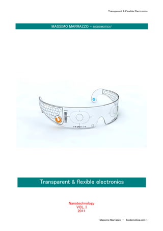
  • 1. Transparent & Flexible Electronics Massimo Marrazzo - biodomotica.com 1 Nanotechnology VOL. I 2011 Transparent & flexible electronics MASSIMO MARRAZZO - BIODOMOTICA®
  • 2. Transparent & Flexible Electronics 2 Massimo Marrazzo - biodomotica.com IIIIIIIInnnnnnnnddddddddeeeeeeeexxxxxxxx Nanotechnology pag.3 Graphene 7 Nanotubes 8 Printed electronics 13 Ink for "printed electronics" 19 Printer for "printed electronics" 21 Transparent and Strong Plastic 24 Transparent Electronics 25 Flexible and trasparent displays 30 Electronic paper / E-paper / E-ink 32 Printed battery 33 Charging batteries without wires 45 WiTricity 46 Solar Energy 48 Seebeck effect - Thermoelectric 55 Printed Memory 77 Printed Antennas 79 Wireless technologies 81 Nanotube Radio 84 Sound 87 Lens 94 Bio-Sensors 98 Virtual Muscles 101 Gecko 106 Mems 113 Ecology 115 Link to transparent electronics 116 Applications of transparent or flexible electronics 117 Invisibility Cloak 125 Acronyms 128 Books 130 Journal Papers 133 Links 134 Show/Convention/Exposition 136 Blogs 136 Toolbox 137 iPad & iPhone applications for Nanotech 138 Android applications for read RSS Nanotech 139 2011 Update 140
  • 3. Transparent & Flexible Electronics Massimo Marrazzo - biodomotica.com 3 NNNNNNNNaaaaaaaannnnnnnnooooooootttttttteeeeeeeecccccccchhhhhhhhnnnnnnnnoooooooollllllllooooooooggggggggyyyyyyyy - http://www.nano.org.uk/whatis.htm What is Nanotechnology? Nanotechnology originates from the Greek word “nanos” meaning “dwarf". A nanometre is one billionth (10-9) of a metre, which is tiny, only the length of ten hydrogen atoms, or about one hundred thousandth of the width of a hair! Although scientists have manipulated matter at the nanoscale for centuries, calling it physics or chemistry, it was not until a new generation of microscopes were invented in the nineteen eighties in IBM, Switzerland that the world of atoms and molecules could be visualized and managed. In simple terms, nanotechnology can be defined as 'engineering at a very small scale', and this term can be applied to many areas of research and development: from medicine to manufacturing to computing, and even to textiles and cosmetics. It can be difficult to imagine exactly how this greater understanding of the world of atoms and molecules has and will affect the everyday objects we see around us, but some of the areas where nanotechnologies are set to make a difference are described below. From Micro to Nano Nanotechnology, in one sense, is the natural continuation of the miniaturization revolution that we have witnessed over the last decade, where millionth of a metre (10-6 m) tolerances (microengineering) became commonplace, for example, in the automotive and aerospace industries enabling the construction of higher quality and safer vehicles and planes. It was the computer industry that kept on pushing the limits of miniaturization, and many electronic devices we see today have nano features that owe their origins to the computer industry — such as cameras, CD and DVD players, car airbag pressure sensors and inkjet printers. ©2008 Institute of Nanotechnology - http://www.crnano.org/whatis.htm What is Nanotechnology? A basic definition: Nanotechnology is the engineering of functional systems at the molecular scale. This covers both current work and concepts that are more advanced. In its original sense, 'nanotechnology' refers to the projected ability to construct items from the bottom up, using techniques and tools being developed today to make complete, high performance products. The Meaning of Nanotechnology When K. Eric Drexler popularized the word 'nanotechnology' in the 1980's, he was talking about building machines on the scale of molecules, a few nanometers wide motors, robot arms, and even whole computers, far smaller than a cell. Drexler spent the next ten years describing and analyzing these incredible devices, and responding to accusations of science fiction. Meanwhile, mundane technology was developing the ability to build simple structures on a molecular scale. As nanotechnology became an accepted concept, the meaning of the word shifted to encompass the simpler kinds of nanometer-scale technology. The U.S. National Nanotechnology Initiative was created to fund this kind of nanotech: their definition includes anything smaller than 100 nanometers with novel properties.
  • 4. Transparent & Flexible Electronics 4 Massimo Marrazzo - biodomotica.com Four Generations Mihail (Mike) Roco of the U.S. National Nanotechnology Initiative has described four generations of nanotechnology development (see chart below). The current era, as Roco depicts it, is that of passive nanostructures, materials designed to perform one task. The second phase, which we are just entering, introduces active nanostructures for multitasking; for example, actuators, drug delivery devices, and sensors. The third generation is expected to begin emerging around 2010 and will feature nanosystems with thousands of interacting components. A few years after that, the first integrated nanosystems, functioning (according to Roco) much like a mammalian cell with hierarchical systems within systems, are expected to be developed. © 2002-2008 Center for Responsible Nanotechnology TM CRN is an affiliate of World Care®, an international, non-profit, 501(c)(3) organization.
  • 5. Transparent & Flexible Electronics Massimo Marrazzo - biodomotica.com 5 - http://en.wikipedia.org/wiki/Nano- Nano- (symbol n) is a prefix in the metric system denoting a factor of 10−9 or 0.000000001. It is frequently encountered in science and electronics for prefixing units of time and length, such as 30 nanoseconds (symbol ns), 100 nanometres (nm) or in the case of electrical capacitance, 100 nanofarads (nF). The prefix is derived from the Greek νάνος, meaning "dwarf", and was officially confirmed as standard in 1960. In the United States, the use of the nano prefix for the farad unit of electrical capacitance is uncommon; capacitors of that size are more often expressed in terms of a small fraction of a microfarad or a large number of picofarads. When used as a prefix for something other than a unit of measure, as in "nanoscience", nano means relating to nanotechnology, or on a scale of nanometres. See nanoscopic scale. SI prefixes Prefix Symbol 10n Decimal Short scale Long scale yotta Y 1024 1000000000000000000000000 Septillion Quadrillion zetta Z 1021 1000000000000000000000 Sextillion Trilliard exa E 1018 1000000000000000000 Quintillion Trillion peta P 1015 1000000000000000 Quadrillion Billiard tera T 1012 1000000000000 Trillion Billion giga G 109 1000000000 Billion Milliard mega M 106 1000000 Million kilo k 103 1000 Thousand hecto h 102 100 Hundred deca da 101 10 Ten 10 0 1 One deci d 10-1 0.1 Tenth centi c 10-2 0.01 Hundredth milli m 10-3 0.001 Thousandth micro ì 10-6 0.000001 Millionth nano n 10-9 0.000000001 Billionth Milliardth pico p 10-12 0.000000000001 Trillionth Billionth femto f 10-15 0.000000000000001 Quadrillionth Billiardth atto a 10-18 0.000000000000000001 Quintillionth Trillionth zepto z 10-21 0.000000000000000000001 Sextillionth Trilliardth yocto y 10-24 0.000000000000000000000001 Septillionth Quadrillionth The International System of Units (SI) specifies a set of unit prefixes known as SI prefixes or metric prefixes. An SI prefix is a name that precedes a basic unit of measure to indicate a decadic multiple or fraction of the unit. Each prefix has a unique symbol that is prepended to the unit symbol. Name Abbrev. Decimal Representative objects with this size scale metre m 100 Height of a 7-year-old child. deci- dm 10-1 Size of our palm. centi- cm 10-2 Length of a bee. milli- mm 10-3 Thickness of ordinary paperclip. micro- ìm 10-6 Size of typical dust particles. nano- nm 10-9 The diametre of a C60 molecule is about 1 nm. pico- pm 10-12 Radius of a Hydrogen Atom is about 23 pm. femto- fm 10-15 Size of a typical nucleus of an atom is 10 fm. atto- am 10-18 Estimated size of an electron
  • 6. Transparent & Flexible Electronics 6 Massimo Marrazzo - biodomotica.com http://commons.wikimedia.org/wiki/Commons:Featured_picture_candidates/Image:Biological_and_technological_scales_compared-en.svg
  • 7. Transparent & Flexible Electronics Massimo Marrazzo - biodomotica.com 7 GGGGGGGGrrrrrrrraaaaaaaapppppppphhhhhhhheeeeeeeennnnnnnneeeeeeee - http://en.wikipedia.org/wiki/Graphene Graphene is a one-atom-thick planar sheet of sp2-bonded carbon atoms that are densely packed in a honeycomb crystal lattice. It can be viewed as an atomic-scale chicken wire made of carbon atoms and their bonds. The name comes from GRAPHITE + ENE; graphite itself consists of many graphene sheets stacked together. Graphene is an atomic-scale chicken wire made of carbon atoms. Integrated circuits Graphene has the ideal properties to be an excellent component of integrated circuits. Graphene has a high carrier mobility, as well as low noise allowing it to be utilized as the channel in a FET. The issue is that single sheets of graphene are hard to produce, and even harder to make on top of an appropriate substrate. Researchers are looking into methods of transferring single graphene sheets from their source of origin (mechanical exfoliation on SiO2 / Si or thermal graphitization of a SiC surface) onto a target substrate of interest. In 2008, the smallest transistor so far, one atom thick, 10 atoms wide was made of graphene. Transparent conducting electrodes Graphene's high electrical conductivity and high optical transparency make it a candidate for transparent conducting electrodes, required for such applications as touchscreens, liquid crystal displays, organic photovoltaic cells, and OLEDs. In particular, graphene's mechanical strength and flexibility are advantageous compared to indium tin oxide, which is brittle, and graphene films may be deposited from solution over large areas.
  • 8. Transparent & Flexible Electronics 8 Massimo Marrazzo - biodomotica.com NNNNNNNNaaaaaaaannnnnnnnoooooooottttttttuuuuuuuubbbbbbbbeeeeeeeessssssss - http://en.wikipedia.org/wiki/Carbon_nanotube 3D model of three types of single-walled carbon nanotubes. Carbon nanotubes (CNTs) are allotropes of carbon with a nanostructure that can have a length-to-diameter ratio greater than 1,000,000. These cylindrical carbon molecules have novel properties that make them potentially useful in many applications in nanotechnology, electronics, optics and other fields of materials science. They exhibit extraordinary strength and unique electrical properties, and are efficient conductors of heat. Inorganic nanotubes have also been synthesized. Their name is derived from their size, since the diameter of a nanotube is in the order of a few nanometers (approximately 1/50,000th of the width of a human hair), while they can be up to several millimeters in length (as of 2008). Nanotubes are categorized as single-walled nanotubes (SWNTs) and multi-walled nanotubes (MWNTs). - http://www.unidym.com/technology/about_carbon.html What are Carbon Nanotubes? Carbon nanotubes (CNTs) are tubular cylinders of carbon atoms that have extraordinary electrical, mechanical, optical, thermal, and chemical properties.
  • 9. Transparent & Flexible Electronics Massimo Marrazzo - biodomotica.com 9 Individual carbon nanotubes can conduct electricity better than copper, possess higher tensile strength than steel, and conduct heat better than diamond. In electronic applications, carbon nanotubes can possess higher mobilities than single crystal silicon. All this in a material that is over 10,000 times thinner than a human hair. There are multiple forms of carbon nanotubes, varying in diameter, length, and in the tendency of the nanotubes to form ropes and bundles of tubes. Some forms of carbon nanotubes are metallic and highly conducting; other forms are semiconducting, and can form the basis of electronic switches. - http://www.unidym.com/technology/about_carbon_more.html CARBON NANOTUBES Carbon nanotubes (fullerene nanotubes) are part of the fullerene family of carbon materials discovered by Dr. Richard E. Smalley and colleagues in 1985. They include single-wall carbon nanotubes (SWNTs), and nested (endohedral or endotopic) SWNTs, i.e., one, two or more tubular fullerenes nested inside another tubular fullerene. Each tubular fullerene is a huge carbon molecule, often having millions of carbon atoms bonded together to form a tiny tube. Carbon nanotube diameters range from about 0.5 to about 10 nanometers (one nanometer = 10-9 meter) and their lengths are typically between a few nanometers and tens of microns (one micron = 10-6 meter). Carbon is a truly remarkable atom. It readily bonds with itself into extended sheets of atoms comprising linked hexagonal rings shown below. Each carbon atom is covalently bonded to its three nearest neighbors.
  • 10. Transparent & Flexible Electronics 10 Massimo Marrazzo - biodomotica.com This unique sheet structure is called graphene. Solid graphite is made up of layers of graphene stacked as shown above. No other element in the periodic table bonds to itself in an extended network with the strength of the carbon-carbon bond, which is among the strongest of chemical bonds. Some of the electrons in the carbon-carbon bonds are free to move about the entire graphene sheet, rather than stay home with their donor atoms, giving the structure good electrical conductivity. The tight coupling between atoms in the carbon- carbon bond provides an intrinsic thermal conductivity that exceeds almost all other materials. As suggested by the carbon nanotube figure above, the structure of a fullerene nanotube is that of a sheet of graphene, wrapped into a tube and bonded seamlessly to itself. This is a true molecule with every atom in its place and very few defects: an example of molecular perfection on a relatively large scale. The special nature of the bonded carbon sheet, the molecular perfection of carbon nanotubes, and their long tubular shape endow them with physical and chemical properties that are unlike those of any other material. These properties include high surface area, excellent electrical and thermal conductivity, and tremendous tensile strength, stiffness, and toughness. In a single tube, every atom is on two surfaces - the inside and the outside, and a single gram of nanotubes has over 2400 m2 of surface area! The nature of the carbon bonding gives the tubes their great tensile strength and electrical and thermal conductivity. The carbon nanotubes' stiffness and toughness derives from their molecular perfection. In most materials the actual observed stiffness and toughness are degraded very substantially by the occurrence of defects in their structure. For example, high strength steel typically fails at about 1% of its theoretical breaking strength. Carbon nanotubes, however, achieve values very close to their theoretical limits because of their perfection of structure - there are no structural defects where mechanical failures can begin! It is, however, the tubular geometry of carbon nanotubes that gives them their most exotic properties. Depending on the orientation of the graphene sheet forming the tube's wall, the tube can be either metallic or semiconducting. The metallic tubes conduct electricity just as metals do and the semiconducting ones have great promise as the basic elements of a new paradigm for electronic circuitry at the molecular level. Basic Structure There are literally hundreds of different carbon nanotube structures. One can identify these structures by thinking of the carbon nanotube as a sheet of graphene wrapped into a seamless cylinder. As one might imagine, there are many ways to wrap a graphene cylinder, and the cylinder can have a wide range of dimensions. Soon after fullerene nanotubes were discovered, a classification scheme was devised to describe the different conformations of graphene cylinders. This classification scheme uses an ordered pair of numbers, (n,m), and is based upon the diagram of graphene shown below. Each carbon atom in the graphene sheet is bonded to three other carbon atoms, forming a Y-shaped vertex of carbon-carbon bonds. In order to make a seamless graphene tube of a uniform diameter, one must wrap the graphene sheet in a way that permits every carbon atom in the cylinder to be bonded to three other carbon atoms where the sheet joins to itself. The number of ways this wrapping can be achieved is countable according to the numbering scheme given in the figure below. The unit vectors of the 2-dimensional graphene lattice are shown as a1 and a2 below. Each vertex that could possibly join to the origin during a wrapping operation is labeled with an ordered pair wherein the first number of the pair is the distance (in lattice repeat units) of the vertex from the origin along a1, and the second number is the distance of the vertex from the origin along a2.
  • 11. Transparent & Flexible Electronics Massimo Marrazzo - biodomotica.com 11 - http://www.unidym.com/technology/cnt_application_electronics.html Transparent Conductive Films One of the more amazing attributes of carbon nanotubes is that they can form films that are highly electrically conductive, but almost completely transparent. The film is only about 50 nanometers thick, and very porous. Under an electron microscope, the film is seen to be a just a few layers of endless carbon nanotube ropes. The films have an ideal conductivity for multiple types of touch screens which have applications including point-of-sale terminals, games, portable computers, cell phones, personal digital assistants and many others. The transparent films used initially for touch screens also reach any application that requires a large-area transparent conductor, including LCD displays, plastic solar cells, and organic LED lighting, and transparent carbon nanotube films have been demonstrated in the laboratory to be effective in all these areas. Printable Transistors The semiconducting properties of carbon nanotubes can be exploited to create printable transistors with extremely high performance. Specifically, researchers have shown CNT-based transistors employing a sparse nanotube network to achieve mobilities of 1 cm2/V-s (Schindler et al., Physica E (2006), while those using an aligned array of single-walled nanotubes can reach as high as 480 cm2/V-s [Kang et al., Nature Nanotech. 2, 230 (2007)]. Nanotubes also prove to be useful additives to polymer-based TFTs and help to overcome some of the shortcomings of those devices. Beyond their performance, such devices are compatible with solution- based printing techniques, which enable dramatic cost savings in such devices as LCDs and OLED-based displays. Field Emission Carbon nanotubes are the best field emitters of any known material. This is understandable, given their high electrical conductivity, and the unbeatable sharpness of their tip. If the tip is placed close to another electrode and a voltage is applied between the tube and electrode, a large electric field builds up near the tip of the tube. The magnitude of the electric field is inversely proportional to the radius of curvature of the tip. Thus the sharper the tip is, the larger the electric field. Even with only a few volts applied to an electrode a few microns away from the nanotube tip, electric fields in the range of a millions of Volts per centimeter will build up near the tip. These fields are large enough to pull a substantial number of electrons out of the tip. As "cold cathode" electron emitters, carbon nanotube films have been shown to be capable of emitting over 4 Amperes per square centimeter. Furthermore, the current is extremely stable [B.Q. Wei, et al. Appl. Phys. Lett. 79 1172 (2001)]. An immediate application of this behavior receiving considerable interest is in field-emission flat-panel displays. Instead of a single electron gun, as in a traditional cathode ray tube display, there is a separate electron gun for each pixel in the display. The high current density, low turn-on and operating voltage, and steady, long-lived behavior make carbon nanotubes ideal field emitters for this application. Other applications utilizing the field-emission characteristics of carbon nanotubes include: high-resolution x-ray sources, general cold-cathode lighting sources, high-performance microwave tubes, lightning arrestors, and electron microscope cathodes. Integrated Circuits Nanotubes might also represent a solution to thermal management problems plaguing the semiconductor industry. As more and more transistors are packed on chips, microprocessors are getting hotter and noisier. The industry is searching for new types of heat sinks to control temperatures on chips. Nanotubes have tremendous thermal conductivity, and a number of firms are developing nanotube-based heat sinks. Due to the unique conducting and semiconducting properties of nanotubes, devices based on individual carbon nanotubes may eventually replace existing silicon devices. For example, several prototypes for future memory devices based on nanotubes have been demonstrated. In light of their high carrying capacity, nanotubes might replace copper interconnects in integrated circuits. Additionally, individual nanotubes have been shown to be superior to existing silicon transistors and diodes. - http://thefutureofthings.com/news/1106/high-speed-carbon-nanotube-based-chips.html High Speed Carbon Nanotube Based Chips A team of electrical engineers from Stanford University and Toshiba have developed nanotube wires that can withstand data transfer speeds comparable to those of commercially available chips. In a paper published in the _Nano Letters" Journal, the researchers reported they had successfully used nanotubes to wire a silicon chip operating at the same speeds as today's processors.
  • 12. Transparent & Flexible Electronics 12 Massimo Marrazzo - biodomotica.com Silicon CMOS integrated circuit with Carbon nanotube interconnect. (Credit: Gael Close Stanford University) - Copyright © 2008 The Future of Things.
  • 13. Transparent & Flexible Electronics Massimo Marrazzo - biodomotica.com 13 PPPPPPPPrrrrrrrriiiiiiiinnnnnnnntttttttteeeeeeeedddddddd eeeeeeeelllllllleeeeeeeeccccccccttttttttrrrrrrrroooooooonnnnnnnniiiiiiiiccccccccssssssss - http://en.wikipedia.org/wiki/Printed_electronics Printed electronics is a set of printing methods used to create electrical devices. Paper's rough surface and high water absorption rate has focused attention on materials such as plastic, ceramics and silicon. Printing typically uses common printing equipment, such as screen printing, flexography, gravure, offset lithography and inkjet. Electrically functional electronic or optical inks are deposited on the substrate, creating active or passive devices, such as thin film transistors or resistors. Printed electronics is expected to facilitate widespread, very low-cost, low-performance electronics for applications such as flexible displays, smart labels, decorative and animated posters, and active clothing that do not require high performance. The term printed electronics is related to organic electronics or plastic electronics, in which one or more inks are composed of carbon-based compounds. These other terms refer to the ink material, which can be deposited by solution-based, vacuum-based or some other method. Printed electronics, in contrast, specifies the process, and can utilize any solution-based material, including organic semiconductors, inorganic semiconductors, metallic conductors, nanoparticles, nanotubes, etc. - http://alislab.com/research/sub01.html Printed electronics (also called electronic printing) is the term for a relatively new technology that defines the printing of electronics on common media such as paper, plastic using standard printing processes. This printing preferably utilizes common press equipment in the graphics arts industry, such as screen printing, flexography, gravure, contact printing and offset lithography. Instead of printing graphic arts inks, families of electrically functional electronic inks (conducting polymer, SWNT, insulator solution, etc) are used to print active devices, such as thin film transistors, electronic paper, and flexible displays. Printed electronics is expected to facilitate widespread and very low-cost electronics useful for applications not typically associated with conventional silicon based electronics, such as flexible displays, RF-ID tags, printing displays, and functional clothing. - http://en.wikipedia.org/wiki/Conductive_polymer Conductive polymers or more precisely intrinsically conducting polymers (ICPs) are organic polymers that conduct electricity. Such compounds may have metallic conductivity or be semiconductors. The biggest advantage of conductive polymers is their processability. Conductive polymers are also plastics, which are organic polymers. Therefore, they can combine the mechanical properties (flexibility, toughness, malleability, elasticity, etc.) of plastics with high electrical conductivity. - http://www.nanowerk.com/spotlight/spotid=1814.php
  • 14. Transparent & Flexible Electronics 14 Massimo Marrazzo - biodomotica.com The fabrication of electronic devices on plastic substrates has attracted considerable recent attention owing to the proliferation of handheld, portable consumer electronics. Plastic substrates possess many attractive properties including biocompatibility, flexibility, light weight, shock resistance, softness and transparency. Achieving high performance electronics or sensors on plastic substrates is difficult, because plastics melt at temperatures above 120 degrees C. Central to continued advances in high-performance plastic electronics is the development of robust methods for overcoming this temperature restriction. Unfortunately, high quality semiconductors (such as silicon) require high growth temperatures, so their application to flexible plastics is prohibited. A group of researchers at the California Institute of Technology now showed that highly ordered films of silicon nanowires can be literally glued onto pieces of plastic to make flexible sensors with state-of-the- art sensitivity to a range of toxic chemicals. These nanowires are crystalline wires made out of doped silicon – the mainstay of the computer industry. By etching nanowires into a wafer of silicon, and then peeling them off and transferring them to plastic, they developed a general, parallel, and scalable strategy for achieving high performance electronics on low cost plastic substrates. Photograph of the flexible sensor chip (Image: Heath Group, Caltech) By Michael Berger, Copyright 2008 Nanowerk LLC - http://www.gizmag.com/go/4749/picture/16223/ By Mike Hanlon September 15, 2005 First polymer electronic transistor produced completely by means of continuous mass printing technology. The finger structure of the source/drain electrodes can be seen, behind them lies the reddish semiconsuctor layer. The gate electrode lies invisibly behind the white insulator layer. Source: [pmTUC] Institute for Print- und Media Technology http://www.tu-chemnitz.de/mb/PrintMedienTech/pminstitut_en/download_en.php - http://printedelectronics.idtechex.com/printedelectronicsworld/en/aboutus.asp
  • 15. Transparent & Flexible Electronics Massimo Marrazzo - biodomotica.com 15 About Printed Electronics World Printed Electronics World provides you with a daily update of the latest industry developments. Launched in May 2007, this free portal covers the progress to printed electronics in all its forms - from transistor circuits to power, sensors, displays, materials and manufacturing. Hosted and written by IDTechEx, the leading printed electronics analyst and event organiser, articles provide commentary, analysis and give a balanced view of the issue. Copyright © 2008 IDTechEx Ltd. - http://www.gizmag.com/biocompatible-flexible-led-array/16708/ Flexible, biocompatible LEDs could light the way for next gen biomedicine By Ben Coxworth October 22, 2010 Researchers from the University of Illinois at Urbana-Champaign have created bio-compatible LED arrays that can bend, stretch, and even be implanted under the skin. While this might cause some people to immediately think _glowing tattoos!", the arrays are actually intended for activating drugs, monitoring medical conditions, or performing other biomedical tasks within the body. Down the road, however, they could also be incorporated into consumer goods, robotics, or military/industrial applications. Many groups have been trying to produce flexible electronic circuits, most of those incorporating new materials such as carbon nanotubes combined with silicon. The U Illinois arrays, by contrast, use the traditional semiconductor gallium arsenide (GaAs) and conventional metals for diodes and detectors. An LED array, transfer printed onto the fingertip of a vinyl glove
  • 16. Transparent & Flexible Electronics 16 Massimo Marrazzo - biodomotica.com Bending with a folded piece of paper Last year, by stamping GaAs-based components onto a plastic film, Prof. John Rogers and his team were able to create the array's underlying circuit. Recently, they added coiled interconnecting metal wires and electronic components, to create a mesh-like grid of LEDs and photodetectors. That array was added to a pre-stretched sheet of rubber, which was then itself encapsulated inside another piece of rubber, this one being bio- compatible and transparent. The resulting device can be twisted or stretched in any direction, with the electronics remaining unaffected after being repeatedly stretched by up to 75 percent. The coiled wires, which spring back and forth like a telephone cord, are the secret to its flexibility. The research was recently published in the journal Nature Materials.
  • 17. Transparent & Flexible Electronics Massimo Marrazzo - biodomotica.com 17 - http://blog.targethealth.com/?p=14473 Roll-to-roll Plastic Displays Oct 22 2010 A new company puts silicon transistors on plastic for flexible displays This plastic material is used as the backing for Phicot’s amorphous silicon electronics. Credit: Phicot
  • 18. Transparent & Flexible Electronics 18 Massimo Marrazzo - biodomotica.com Organic electronics (see also Printed electronic) - http://en.wikipedia.org/wiki/Organic_electronics Organic electronics, or plastic electronics, is a branch of electronics that deals with conductive polymers, plastics, or small molecules. It is called 'organic' electronics because the polymers and small molecules are carbon-based, like the molecules of living things. This is as opposed to traditional electronics which relies on inorganic conductors such as copper or silicon. Conductive polymers are lighter, more flexible, and less expensive than inorganic conductors. This makes them a desirable alternative in many applications. It also creates the possibility of new applications that would be impossible using copper or silicon. Organic electronics not only includes organic semiconductors, but also organic dielectrics, conductors and light emitters. New applications include smart windows and electronic paper. Conductive polymers are expected to play an important role in the emerging science of molecular computers. In general organic conductive polymers have a higher resistance and therefore conduct electricity poorly and inefficiently, as compared to inorganic conductors. Researchers currently are exploring ways of "doping" organic semiconductors, like melanin, with relatively small amounts of conductive metals to boost conductivity. However, for many applications, inorganic conductors will remain the only viable option. Organic electronics can be printed.
  • 19. Transparent & Flexible Electronics Massimo Marrazzo - biodomotica.com 19 IIIIIIIInnnnnnnnkkkkkkkk ffffffffoooooooorrrrrrrr ““““““““pppppppprrrrrrrriiiiiiiinnnnnnnntttttttteeeeeeeedddddddd eeeeeeeelllllllleeeeeeeeccccccccttttttttrrrrrrrroooooooonnnnnnnniiiiiiiiccccccccssssssss”””””””” - http://www.printelectronicnews.com/2820/epoxy-ink-for-printed-electronics/ Fine-Line Epoxy Ink Recommended for Printed Electronics Applications December 2nd, 2010 Creative Materials, Inc., introduces 125-26, an exceptional conductive ink for screen- printing circuits with fine- line widths and spaces. Creative Materials is expanding its line of products for the printed electronics market. Our newest product, 125-26A/B119-44 is a flexible two-part epoxy ink that features superior adhesion to ITO- coated surfaces and other low surface-energy substrates. This product has been used successfully in printed electronics applications and is recommended where high-performance on coated substrates is necessary. - http://www.printelectronicnews.com/2732/new-film-technologies/ New film technologies for printed polymer electronics developed October 22nd, 2010 Conductive nano inks for flexible circuits Bayer MaterialScience develops conductive and formable nano inks for use in areas such as printed polymer electronics under the BayInk® name. These can be applied digitally using Depending on the process, it is possible to apply line widths with a resolution of less than 30 micrometers that are no longer visible to the human eye. This enables conductor tracks, contacts and electrodes to be applied much more easily and effectively than with conventional methods, which are mostly more complicated and more energy- and material-intensive. The inks ad here to a very wide range of plastic films such as Makrofol® and Bayfol® and other flexible materials, as well as to rigid substrates. The range of applications is wide – for example, as invisible conductor tracks they can be used to simplify the complex design of touchscreens. Customized service along the entire process chain. - http://www.nanotech-now.com/news.cgi?story_id=36811 Conductive nano inks for printed electronics Leverkusen | February 17th, 2010 The two conductive inks BayInk® TP S and BayInk® TP CNT from Bayer MaterialScience have been developed primarily for use in the growing “printed electronics” market. These new inks boast excellent adhesion to plastic films, other flexible substrates, glass, silicon and indium tin oxide. - http://www.nanowerk.com/news/newsid=16884.php Methode's Inkjet Printable Conductive Ink Allows Printing of Circuits on Polyester with No Secondary Curing June 24, 2010 (Nanowerk News) Methode Development Company, a business unit of Methode Electronics, Inc., announces that its conductive inkjet printable ink can now print circuits directly onto treated polyesters. The ink, formulated for thermal and piezo inkjet systems, makes it possible for engineers to print working electrical circuits, right from their desktops – facilitating product development, prototyping, and manufacturing processes. With this technology, scale-up for high volume manufacturing can be easily achieved.
  • 20. Transparent & Flexible Electronics 20 Massimo Marrazzo - biodomotica.com - http://www.inktec.com/english/product_info/electronic_tec.asp Transparent Electronic Conductive TEC is the acronym of _Transparent Electronic Conductive," and one of the salient features of that TEC ink is its transparency at liquid phase. It means TEC is non-particle type ink before sintering and specially designed by InkTec, which is a world-class research and manufacturing company of inkjet applications. - http://nanotechweb.org/cws/article/tech/33180 Inkjet prints transparent CNT film. Transparent conductive film for use in displays is one of the headline applications for carbon nanotubes (CNTs). The interconnected material is seen as being more robust than today's ITO electrodes and could prove a popular choice for flexible devices, but the challenge is to bring down production costs. - http://www.epson.co.jp/e/newsroom/news_2004_11_01.htm Epson Inkjet Technology Used to Fabricate World's First Ultra-Thin Multilayer Circuit Board. Epson recently succeeded in producing a 20-layer circuit board sample by using an inkjet system to alternately "draw" patterns and form layers on the board using two types of ink: a conductive ink containing a dispersion of silver micro-particles measuring from several nanometers to several tens of nanometers in diameter, and a newly developed insulator ink. Copyright © 2008 SEIKO EPSON CORP - https://buffy.eecs.berkeley.edu/PHP/resabs/resabs.php?f_year=2005&f_submit=one&f_absid=100770 High-Performance All-Inkjet-Printed Transistors for Ultra-low-cost RFID Applications Dec 16, 2010 Alejandro De La Fuente Vornbrock, Steven Edward Molesa, David Howard Redinger and Steven K. Volkman (Professors Ali Niknejad and Vivek Subramanian) Semiconductor Research Corporation, Defense Advanced Research Projects Agency and National Science Foundation Printed electronics will enable the development of ultra-low-cost RFID circuits for use as electronic barcodes, since it eliminates the need for lithography, vacuum processing, and allows the use of low-cost web manufacturing. Recently, there have been several demonstrations of printed transistors with mobilities approaching or exceeding 1 cm2/V-s; however, all such devices have been fabricated using silicon substrates with thermally grown oxides or using vacuum sublimated materials. In order to achieve ultra low cost, performance must be maintained without silicon substrates or vacuum processing. - http://www.laserfocusworld.com/display_article/206960/12/none/none/Feat/Semiconductor-ink-advances-flexible-displays Semiconductor ink advances flexible displays The technique being developed fabricates devices using high-volume inkjet printing to replace the photolithographic techniques used to create the thin-film-transistor backplane circuits used in displays. A liquid-based organic semiconductor material, developed by Xerox researchers, is used to print the semiconductor channel layers for large-area transistor arrays.By Beng Ong - Research fellow and manager, Advanced Materials and Organic Electronics Group, Xerox Research Centre of Canada. Copyright © 2007: PennWell Corporation, Tulsa, OK
  • 21. Transparent & Flexible Electronics Massimo Marrazzo - biodomotica.com 21 PPPPPPPPrrrrrrrriiiiiiiinnnnnnnntttttttteeeeeeeerrrrrrrr ffffffffoooooooorrrrrrrr ““““““““pppppppprrrrrrrriiiiiiiinnnnnnnntttttttteeeeeeeedddddddd eeeeeeeelllllllleeeeeeeeccccccccttttttttrrrrrrrroooooooonnnnnnnniiiiiiiiccccccccssssssss”””””””” - http://www.ntera.com/technology/printing_processes.php Web-Fed (Roll-to-Roll) Printed NCD Displays on Flexible Substrate Printing Processes NanoChromics Ink Systems are compatible with existing printing equipment and processes. Sheet or Web-fed Screen Printing Flexographic Printing Inkjet Printing Leveraging additive print processes, NanoChromics Ink Systems can be combined with other printed electronic technologies (and traditional graphics inks) on the same substrate. Compatibility with existing, widely available printing equipment minimizes capital investment for traditional graphics printers looking to expand into printed electronics and functional media.
  • 22. Transparent & Flexible Electronics 22 Massimo Marrazzo - biodomotica.com - http://www.citala.com/index.php/flexible-display-technology/Roll-To-Roll-Manufacturing.html Roll To Roll Manufacturing Citala, US-based roll-to-roll (R2R) manufacturing is state-of-the art with a track record of reliability. Citala was one of the first companies to offer genuine R2R manufacturing, enabling the production of large, cost-effective quantities. R2R enables solutions for patterning, coating, cutting, and combining different layers of customizable displays. Citala can manufacture flexible displays and optical shutters using the same line. Citala's R2R-schematic diagram - © Copyright 2008 Citala. All Rights Reserved - http://www.xenoncorp.com/print_mkt.html PHOTONIC SINTERING OF NANOPARTICLE INKS ON LOW- TEMPERATURE SUBSTRATES: PULSED LIGHT EXCELS The world of printed electronics is moving out of R&D and into production, and new developments in materials—particularly nanoparticle inks and photonic curing from Xenon Corporation—are in the driver’s seat. Here’s what’s happening: 1.) Functionally conductive inks and coatings now contain nanoparticles that permit the use of low-cost substrates such as paper, PET and polyethylene films. 2.) New developments allow inkjets and screen printers to use silver, gold and most recently, lower-cost copper nanoparticle inks. 3.) It is now possible to print at room temperature on flexible substrates such as printed circuit boards. Here’s the photonic curing contribution: The challenge has long been heat. How do you sinter or anneal nanoparticle inks at substrate temperatures, which are typically below 160C? Xenon’s photonic pulsed light curing answers this challenge. High energy peak pulses, delivered in milliseconds, quickly heat only the inks and not the substrates. The high energy removes the solvent, leaving only the metal flakes which are sintered or annealed, while the substrate is unaffected. This speed allows copper inks to be sintered too quickly for a surface oxide layer to develop, so conductivity is improved. - http://www.oled-display.net/oled-inkjet-printing CDT is sole supplier of the Litrex range of Ink Jet. Cambridge Display Technology have also partnered industry leaders across the globe to offer a fully inclusive ink jet package. To support the Litrex printer range CDT can offer materials, print heads, know-how and skills development packages. More about OLED Inkjet Printing and PLED at http://www.cdtltd.co.uk
  • 23. Transparent & Flexible Electronics Massimo Marrazzo - biodomotica.com 23 - http://www.litrex.com/index.asp?sect=5&page=12 The Litrex _ precision inkjet printer is a low-cost, compact system for research and development of OLED/LEP, LCD, printed electronics, and biomaterial applications. - http://www.dimatix.com/ Dimatix is driving a revolution in micro-production technology that will deliver a new generation of applications in imaging, electronics and the biosciences. - http://www.dea.brunel.ac.uk/cleaner/Electronics_Projects/Handbook_1.htm Over four years research work at Brunel University has demonstrated the feasibility of manufacturing electrical circuit interconnect via the established printing technology of offset lithography. It has been shown that offset- lithography can be used as a process for manufacture of low specification electrical interconnect, leading to reduced production time and raw material use when compared to conventional thick film printing approaches. - http://www.dea.brunel.ac.uk/cleaner/Electronics_Projects/Handbook_2.htm © 2008 Cleaner Electronics Research Group Conventional and Lithographically printed circuit boards for telephone assembly. This demonstrator surpassed all others in complexity and processor speed. - http://www.engr.uiuc.edu/news/index.php?xId=074108960714 'Nanonet' circuits closer to making flexible electronics reality By Emil Venere, Purdue University Together, researchers at Illinois and Purdue have overcome a major obstacle in producing transistors from networks of carbon nanotubes, a technology that could make it possible to print circuits on plastic sheets for applications including flexible displays and an electronic skin to cover an entire aircraft to monitor crack formation.
  • 24. Transparent & Flexible Electronics 24 Massimo Marrazzo - biodomotica.com TTTTTTTTrrrrrrrraaaaaaaannnnnnnnssssssssppppppppaaaaaaaarrrrrrrreeeeeeeennnnnnnntttttttt aaaaaaaannnnnnnndddddddd SSSSSSSSttttttttrrrrrrrroooooooonnnnnnnngggggggg PPPPPPPPllllllllaaaaaaaassssssssttttttttiiiiiiiicccccccc Strong, Light, Transparent Plastic - http://thefutureofthings.com/news/1060/strong-light-transparent-plastic.html Researchers from the University of Michigan (UM) have developed a composite plastic, which they say is strong as steel, but much lighter and transparent. The scientists name several possible applications for their invention. The composite plastic could be used in the making of stronger and lighter armor for soldiers and police forces and for protecting their vehicles. The material could also be used in micro-electromechanical devices, in micro-fluidics and biomedical sensors, in valves, and in unmanned aircrafts. Copyright © 2009 The Future of Things. All rights reserved - http://www.trnmag.com/Photos/2008/033108/Flexible%20silicon%20circuits%20Image.html Flexible silicon Stretchable and bendable computer circuits made from ordinarily brittle single-crystal silicon promise flexible electronic devices that perform at nearly the same level as today's rigid computer chips. © Copyright Technology Research News, LLC 2000-2008. All rights reserved. - http://www.news.uiuc.edu/news/08/0327electronics.html Foldable and stretchable, silicon circuits conform to many shapes - http://www.wisegeek.com/what-is-the-difference-between-silicon-and-silicone.htm Difference Between Silicon and Silicone
  • 25. Transparent & Flexible Electronics Massimo Marrazzo - biodomotica.com 25 TTTTTTTTrrrrrrrraaaaaaaannnnnnnnssssssssppppppppaaaaaaaarrrrrrrreeeeeeeennnnnnnntttttttt EEEEEEEElllllllleeeeeeeeccccccccttttttttrrrrrrrroooooooonnnnnnnniiiiiiiiccccccccssssssss - http://www.indiastudychannel.com/resources/98936-Transparent-Electronics-or-Invisible-Electronics.aspx Transparent Electronics -- or Invisible Electronics Dec 2009 By Pratima Transparent electronics is a emerging technology, which is satisfying the requirements of everything invisible or multi-purpose objects. What is Transparent Electronics? Its just Technology for next generation of optoelectronic devices and employs wide band-gap semiconductors for the realization of invisible circuits. Oxide semiconductors are very interesting materials because they combine simultaneously high/low conductivity with high visual transparency. How it works? Transparent oxide semiconductor based transistors have recently been proposed using as active channel intrinsic zinc oxide (ZnO). The main advantage of using ZnO deals with the fact that it is possible to growth at/near room temperature high quality polycrystalline ZnO, which is a particular advantage for electronic drivers, where the response speed is of major importance. Besides that, since ZnO is a wide band gap material (3.4 eV), it is transparent in the visible region of the spectra and therefore, also less light sensitive. Applications: They have been widely used in a variety of applications like: 1.antistatic coatings 2.touch display panels 3.solar cells, 4.flat panel displays 5.heaters 6.defrosters 7.optical coatings etc - http://kn.theiet.org/magazine/issues/1009/transparent-electronics-1009.cfm Transparent electronics look to use in smart objects June 2010 By Chris Edwards Transparent electronic materials will make it possible to build a new generation of smart objects. After crash-landing on Mars in the 2000 movie 'Red Planet', Val Kilmer tries to work out where he and his team have wound up on the surface. So, he unrolls a see-through computer that tries to match the local landscape with the images collected by scores of unmanned Mars probes over the years. It was a bomb at the box office. Ten years on, 'Red Planet' is not showing much sign of becoming a cult classic and ultimately profitable like 'Blade Runner'. But it's still inspiring engineers to work out how to make a roll-up, see-through map. Tolis Voutsas, director of the materials and devices applications lab at Sharp Laboratories of America, says: ''Red Planet' was shown in 2000. And we still don't have technology to do this. But thanks to Hollywood we still have the vision.' Director Antony Hoffman reckoned it might take a while to realise the transparent map. 'Red Planet' was set in 2056. Engineers such as Chris Bower, principal scientist at Nokia's research centre in Cambridge, are hoping that they can develop something similar much more quickly. Working on morph A couple of years ago, Nokia unveiled what it called the Morph concept. A set of videos showed what the portable computer and phone of the future might look like. Bower explained the idea at the Printed Electronics conference in Dresden in April: 'You can take a standard candy-bar phone and transform it. You can wrap it around your wrist so that it becomes a wearable device. 'We are working hard to enable the Morph concept. We are trying to build a library of functional surface materials that provide the ability to change colour or haptic feedback. We also need compliancy to reshape
  • 26. Transparent & Flexible Electronics 26 Massimo Marrazzo - biodomotica.com the device, with flexible and even stretchable displays. And transparency is something we require,' says Bower, showing a Photoshop-assisted mockup of Nokia's take on the transparent navigator. The roll-up map is not the only applications for see-through electronics. Douglas Keszler of Oregon State University, a leading researcher into transparent metal oxides, reckons these materials will find uses in car dashboards and windows to provide extra real estate for computer circuits. Carbon nanotubes and plastics are vying with metal oxides for a role in transparent electronics, but the metals have a solid lead historically. 'We believe metal oxides can enable transparent electronics and they have been around for some time,' says Flora Li, research associate at the University of Cambridge. In the Second World War, aircraft makers used transparent conductive oxides to deliver heat to windshields to keep them free of ice. Indium tin oxide (ITO) has become the one material that appears almost everywhere as a conductive coating for flat-screens and touchscreens. Unfortunately, the key component, indium, is a very rare and expensive metal, giving researchers a strong incentive to find other options. Peter Harrop, chairman of analyst firm IDTechEx, says: 'It's a defeat that indium tin oxide is still used for transparent electronics. There are replacements but they need to gain traction. That is a big opportunity for a lot of people.' Li says ITO represents the first generation of transparent electronics, forming just passive conductors on the surface of screens. 'The phase we are in now, we consider the second generation, allowing us to fabricate discrete transparent components,' she claims. The coming third generation will put active transparent components into many more devices. Thin-film transistors made out of metal oxides date back to the the 1960s but it's only since the late 1990s that research has shown that it is possible to create a library of standard components that you can see through. Keszler points to a paper on the creation of a p-type transistor by Hiroshi Kawazoe and colleagues at the Tokyo Institute of Technology in 1997 as the birth of modern transparent electronics. Up to that point, all the conductors were n-type. With the two types available, it became feasible to build thin-film diodes and transistors. There is a reason why transparent metal oxides are not more widely used in electronics. As with the organic polymers used in printed electronics, electrons do not move easily through most of them. According to Keszler, the best materials have a conductivity more than ten times worse than the contact metals used today in silicon chips. Li says even with this lower performance, there is still a useful role for these devices. She compares metal oxides to lower-grade forms of silicon used in flat-panel displays, such as polycrystalline and amorphous, non-crystalline silicon, often called alpha-silicon. 'Polysilicon gives you great mobility. But you need to use really high temperatures to get this. Alpha-silicon you can make at much lower temperatures but at the expense of lower mobility. This is where we believe transparent metal oxides fit in: filling a gap between organic materials and alpha-silicon in terms of cost and performance,' says Li. Whereas alpha-silicon generally has a mobility of around 1cm/Vs, researchers have managed to achieve around 30cm'/Vs for the widely available material zinc oxide, which is still five times lower than the polysilicon used in high-end displays but is usable. Mobility is only one of the concerns that researchers have with metal oxides. Sharp worked with startup Inpria, which Keszler co-founded, on indium gallium zinc oxide transistors. 'However, the current doesn't saturate,' says Voutsas, in the way that it should for a workable transistor. 'And the threshold voltage is high. That is why you don't see a product that uses amorphous-oxide TFTs.' As with the the transistor, researchers are working with a range of metals in the hope of finding combinations that work. Li says many of these materials are binary oxides that are difficult to produce reliably using sputtering - the balance between the two metals in the oxide varies, disrupting its ability to conduct electricity.
  • 27. Transparent & Flexible Electronics Massimo Marrazzo - biodomotica.com 27 Like silicon-based processes, the metals can migrate into other layers, which Li found with indium zinc oxide and hafnium oxide gates. 'We found the indium migrated into the hafnium layer and destroyed the device. What we found really works with indium zinc is aluminium,' says Li. On the other hand, zinc oxides seem to work well with hafnium oxide. With work continuing on indium-based oxides, materials scientists have yet to find a genuine low-cost, easily available winner in transparent conductive oxides. 'But we think that this is one of the technologies that will emerge soon,' Voutsas concludes. - http://www.technologyreview.com/computing/21964/?a=f High-quality, clear graphene films are a leap toward bendable OLED displays. Korean researchers have found a way to make large graphene films that are both strong and stretchy and have the best electrical properties yet. Prachi Patel-Predd - © 2009 - .technologyreview.com © 2009 Ji Hye Hong - http://www.sciencenews.org/view/access/id/39865/title/Graphene_from_gases_for_new,_bendable_electronics_ Graphene from gases for new, bendable electronics Flexible, translucent and ultrathin, layers of carbon atoms called graphene are also excellent electrical conductors that could find use in flexible computer displays, molecular electronics and new wireless communications. Making high-quality graphene sheets is usually a slow, painstaking process, but now several research groups have discovered ways to make patterned graphene circuits using techniques borrowed from microchip manufacturing, which can be scaled up for mass production. By Patrick Barry - ©2009 - .sciencenews.org - http://chem.skku.edu/graphene/ SKKU Graphene Research Laboratory - http://www.nanowerk.com/spotlight/spotid=8787.php New work at the University of Southern California (USC) has now demonstrated the great potential of massively aligned single-walled carbon nanotubes for high-performance transparent electronics. "We fabricated transparent thin-film transistors on both rigid and flexible substrates with transfer printed aligned carbon nanotubes as the active channel and indium-tin oxide as the source, drain, and gate electrodes," Chongwu Zhou, Jack Munushian Associate Professor in USC's Department of Electrical Engineering, tells Nanowerk. "We have fabricated these transistors through low-temperature processing, which allowed device fabrication even on flexible substrates." By Michael Berger. Copyright 2008 Nanowerk LLC
  • 28. Transparent & Flexible Electronics 28 Massimo Marrazzo - biodomotica.com - http://pubs.acs.org/doi/pdf/10.1021/nn800434d Transparent Electronics Based on Transfer Printed Aligned Carbon Nanotubes on Rigid and Flexible Substrates Fumiaki N. Ishikawa, Hsiao-kang Chang, Koungmin Ryu, Po-chiang Chen, Alexander Badmaev, Lewis Gomez De Arco, Guozhen Shen and Chongwu Zhou* Department of Electrical Engineering, University of Southern California, Los Angeles, California 90089 ACS Nano, Article ASAP DOI: 10.1021/nn800434d Publication Date (Web): December 10, 2008 Report high-performance fully transparent thin-film transistors (TTFTs) on both rigid and flexible substrates. - http://www.eurekalert.org/pub_releases/2008-12/uosc-urp121608.php USC researchers print dense lattice of transparent nanotube transistors on flexible base It's a clear, colorless disk about 5 inches in diameter that bends and twists like a playing card, with a lattice of more than 20,000 nanotube transistors capable of high-performance electronics printed upon it using a potentially inexpensive low-temperature process. Its University of Southern California creators believe the prototype points the way to such long sought after applications as affordable "head-up" car windshield displays. The lattices could also be used to create cheap, ultra thin, low-power "e-paper" displays. ©2008 www.eurekalert.org - http://www.nanowerk.com/spotlight/spotid=2062.php Transparent and flexible electronics with nanowire transistors Thin-film transistors (TFTs) and associated circuits are of great interest for applications including displays, large-area electronics and printed electronics (e.g. radio-frequency identification tags - RFID). Well- established TFT technologies such as amorphous silicon and poly-silicon are well-suited for many current applications - almost all mobile phone color screens use them - but face challenges in extensions to flexible and transparent applications. In addition, these TFTs have modest carrier mobilities, a measure of the velocity of electrons within the material at a given electric field. The modest mobility corresponds to a modest operating speed for this class of TFTs. Organic TFTs are generally better suited for flexible applications, and can be made transparent. However, mobilities in organic TFTs are generally quite low, restricting the speed of operation and requiring relatively large device sizes. Researchers at Purdue University, Northwestern University, and the University of Southern California now have reported nanowire TFTs that have significantly higher mobilities than other TFT technologies and therefore offer the potential to operate at much higher speeds. Alternatively, they can be fabricated using much smaller device sizes, which allows higher levels of integration within a given chip area. They also provide compatibility with a variety of substrates, as well as the potential for room-temperature processing, which would allow integration of the devices with a number of other technologies (e.g. for displays). "We have demonstrated fully-transparent thin-film transistors (TFTs) on both glass and flexible plastic substrates" Dr. David B. Janes tells Nanowerk. Image of NWTs on a plastic substrate, showing the optical clarity and mechanical flexibility. Arrows point to the transistor array regions (Image: Dr. Janes)
  • 29. Transparent & Flexible Electronics Massimo Marrazzo - biodomotica.com 29 http://www.innovations-report.com/html/reports/physics_astronomy/clear_future_electronics_transparent_memory_device_124145.html The Clear Future of Electronics: Transparent Memory Device A group of scientists at Korea Advanced Institute of Science and Technology (KAIST) has fabricated a working computer chip that is almost completely clear -- the first of its kind. The new technology, called transparent resistive random access memory (TRRAM), is described in this week's issue of the journal Applied Physics Letters, which is published by the American Institute of Physics. 11.12.2008 - http://www.nanowerk.com/spotlight/spotid=1858.php Electronics can be so transparent One of the newly emerging areas of semiconductor technology is the field of transparent electronics. These thin-film materials hold the promise of a new class of flexible and transparent electronic components that would be more environmentally benign than current electronics. However, the emerging transparent electronics technology is facing manufacturing problems: current fabricating processes do not separate the device manufacturing from material synthesis. The transparent electronic materials, which are largely inorganic oxides. are directly deposited on the device substrate under harsh conditions which may cause damage to the existing layer or flexible substrate. The etching of small dimension oxide multilayer is also difficult due to the low selectivity of the etching recipe. New research results demonstrate that nanofabrication techniques could solve these problems. A group of researchers from Clarkson University and Pacific Northwest National Laboratory report that clear nanocrystals can serve as the appropriate electronic materials in the transparent device. "The purpose of our work is to demonstrate the fabrication of transparent devices using nanofabrication and nanomaterials" Dr. Feng Hua tells to Nanowerk. By Michael Berger, Copyright 2008 Nanowerk LLC - http://techon.nikkeibp.co.jp/article/HONSHI/20071024/141211/ Transparent Electronic Products Soon a Reality Since the arrival of low-cost transparent transistors, R&D into transparent electronics has progressed rapidly. It will soon be possible, for instance, to embed transparent electronic circuits into large areas like windows, enabling the display of video imagery. Copyright © 1995-2008 Nikkei Business Publications, Inc. - http://dx.doi.org/doi:10.1038/nnano.2007.151 By Michael Berger, Copyright 2008 Nanowerk LLC - http://nanoarchitecture.net/article/nanotubes-enable-flexible-transparent-electronics Nanotubes Enable Flexible, Transparent Electronics Flexible electronics have taken an important leap forward with the development of a new type of flexible, transparent electrode made using carbon nanotubes (CNTs). Jackson State University researchers made the electrode by applying boron-doped CNTs to glass and polymer film surfaces. The devices are 89% transparent to visible light and are robust; they maintain their conducting properties even after being folded and exposed to harsh environmental conditions. - http://www.azom.com/News.asp?NewsID=7446 Invisible Electronics Northwestern University researchers report that by combining organic and inorganic materials they have produced transparent, high-performance transistors that can be assembled inexpensively on both glass and plastics. - http://npl.postech.ac.kr/?mid=Trans_Electronic Advanced Display Nanodevice Transparent Thin film transistor(TFT) - http://oregonstate.edu/dept/ncs/newsarch/2006/Feb06/license2.htm OSU Licenses New Transparent Electronics to HP Scientists and engineers at Oregon State University have developed a new class of materials that can be used to create safe, inexpensive and transparent electronic circuits, and licensed the exclusive rights to develop and market products based on this technology to HP.
  • 30. Transparent & Flexible Electronics 30 Massimo Marrazzo - biodomotica.com FFFFFFFFlllllllleeeeeeeexxxxxxxxiiiiiiiibbbbbbbblllllllleeeeeeee aaaaaaaannnnnnnndddddddd ttttttttrrrrrrrraaaaaaaassssssssppppppppaaaaaaaarrrrrrrreeeeeeeennnnnnnntttttttt ddddddddiiiiiiiissssssssppppppppllllllllaaaaaaaayyyyyyyyssssssss For more info about this please see: Nanotechnology vol.2 Technology for E-books Readers (B/W & colors display) www.biodomotica.com/public/e-paper_e-book.pdf Flexible Display - http://www.crunchgear.com/2010/05/26/video-sonys-new-super-thin-oled-display-wraps-around-a-pencil/ - http://forum.dailymobile.se/index.php?topic=34521.0
  • 31. Transparent & Flexible Electronics Massimo Marrazzo - biodomotica.com 31 Transparent TFT-LCD - http://techpatio.com/2009/mobiles/sony-ericsson/sony-ericsson-xperia-pureness-600-euro-november-uk-price Transparent OLED - http://www.engadget.com/2010/01/07/samsungs-14-inch-transparent-oled-laptop-video/
  • 32. Transparent & Flexible Electronics 32 Massimo Marrazzo - biodomotica.com EEEEEEEElllllllleeeeeeeeccccccccttttttttrrrrrrrroooooooonnnnnnnniiiiiiiicccccccc ppppppppaaaaaaaappppppppeeeeeeeerrrrrrrr //////// EEEEEEEE--------ppppppppaaaaaaaappppppppeeeeeeeerrrrrrrr //////// EEEEEEEE--------iiiiiiiinnnnnnnnkkkkkkkk®®®®®®®® For more info about this please see: Nanotechnology vol.2 Technology for E-books Readers (B/W & colors display) www.biodomotica.com/public/e-paper_e-book.pdf by Emily Cooper - http://www.cooperhawk.com/contact.htm
  • 33. Transparent & Flexible Electronics Massimo Marrazzo - biodomotica.com 33 PPPPPPPPrrrrrrrriiiiiiiinnnnnnnntttttttteeeeeeeedddddddd bbbbbbbbaaaaaaaatttttttttttttttteeeeeeeerrrrrrrryyyyyyyy - http://www.gizmag.com/worlds-smallest-battery-created/17237/ World’s smallest battery created By Darren Quick December 2010 Nano Battery A tin oxide anode contorts in response to ions flowing in as the battery charges. Sandia Labs http://www.popsci.com/science/article/2010-12/lithium-ion-batteries-swell-and-contort-while-charging-new-study-shows Because battery technology hasn’t developed as quickly as the electronic devices they power, a greater and greater percentage of the volume of these devices is taken up by the batteries needed to keep them running. Now a team of researchers working at the Center for Integrated Nanotechnologies (CINT) is claiming to have created the world’s smallest battery, and although the tiny battery won’t be powering next year’s mobile phones, it has already provided insights into how batteries work and should enable the development of smaller and more efficient batteries in the future. The tiny rechargeable, lithium-based battery was created by a team led by Sandia National Laboratories researcher Jianyu Huang. It consists of a bulk lithium cobalt cathode three millimeters long, an ionic liquid electrolyte, and has as its anode a single tin oxide (Sn02) nanowire 10 nanometers long and 100 nanometers in diameter – that’s one seven-thousandth the thickness of a human hair. Because nanowire-based materials in lithium-ion batteries offer the potential for significant improvements in power and energy density over bulk electrodes the researchers wanted to gain an understanding of the fundamental mechanisms by which batteries work. They therefore formed the battery inside a transmission electron microscope (TEM) so they could study the charging and discharging of the battery in real time and at atomic scale resolution. By following the progression of the lithium ions as they travel along the nanowire, the researchers found that during charging the tin oxide nanowire rod nearly doubles in length. This is far more than its diameter increases and could help avoid short circuits that may shorten battery life. This unexpected finding goes against the common belief of workers in the field that batteries swell across their diameter, not longitudinally. “Manufacturers should take account of this elongation in their battery design,” Huang said. “These observations prove that nanowires can sustain large stress (>10 GPa) induced by lithiation without breaking, indicating that nanowires are very good candidates for battery electrodes,” he added. Atomic-scale examination of the charging and discharging process of a single nanowire had not been possible before because the high vacuum in a TEM made it difficult to use a liquid electrolyte. Huang’s group overcame this problem by demonstrating that a low-vapor-pressure ionic liquid – essentially molten salt – could function in the vacuum environment. This means that although the work was carried out using tin oxide nanowires, Huang says the experiments could be extended to other materials systems, either for cathode or anode studies. “The methodology that we developed should stimulate extensive real-time studies of the microscopic processes in batteries and lead to a more complete understanding of the mechanisms governing battery performance and reliability,” he said. “Our experiments also lay a foundation for in-situ studies of electrochemical reactions, and will have broad impact in energy storage, corrosion, electrodeposition and general chemical synthesis research field.” The research team’s work is reported in the December 10 issue of the journal Science.
  • 34. Transparent & Flexible Electronics 34 Massimo Marrazzo - biodomotica.com - http://www.energyharvestingjournal.com/articles/printed-lithium-reshaping-battery-00002104.asp Energy Scavenging, Power Scavenging - Making small electronic and electric devices self-sufficient Mar 2010 | Japan Printed lithium reshaping battery In February 2010, ITSUBO Advanced Materials Innovation Center and Hatanaka Electric in Japan announced a large area printed lithium polymer battery that can be reshaped as shown in the pictures. This is the statement from Mie Prefecture Industrial Support Center for the Promotion of Education and Science, Ministry of Industry-Academia Collaboration Urban Areas (a development in the Mie Ise Bay area). "This development of advanced materials and innovation creates a new generation all-solid polymer lithium secondary battery. It is a world first because the all-solid polymer lithium secondary battery employs a printing process. This battery, involving new electrode material and electrode interface control technology and a new polymer electrolyte, plus a separator, avoids the safety and reliability challenges of manufacturing polymer electrolyte lithium ion secondary batteries. A safe, thin, bendable, large area battery has resulted, which offers ease of stacking. Such batteries are welcome as the printed electronics sector is expected to grow rapidly. Development of this cell is continuing at the Principal Research and Development Center for Next Generation Batteries, Mie University, Mie Prefecture Industrial Research Institute (Kinseimatekku Co., Ltd., Kurehaerasutoma Co., Ltd., Shin-Co., Ltd., Toppan Printing Co., Ltd., Myeongseong Chemical Co., Ltd.). It has been jointly conducted by the government and academia." Photos prototype polymer lithium secondary batteries Prototype battery performance "Cell size A6 (external dimension), cell thickness 450µm (external dimension) Initial charge and discharge efficiency of 99% Initial capacity of 45mAh (electrode material utilization efficiency of 80%) Operating voltage 1.8 V (voltage at 50% depth of discharge) Discharge rate of 0.02C ~ 1.0C of more than 100 cycle times (the current ongoing evaluation) Operating Temperature 0 ~ 25 C° In future, we will dramatically improve the performance of the battery cell structure design and optimization of polymer electrolyte interface control electrode materials." Second generation lithium batteries that are safer and have better performance are incorporated in the Lightning Car Company's Lightning sports car, the KleenSpeed Technologies 200mph Formula One car, the Hawkes Ocean Technologies Deepflight submarines, the PC-Aero pure electric aircraft etc. but even more powerful batteries will be welcome. For more read : Energy Harvesting and Storage for Electronic Devices 2009-2019 - http://newenergyandfuel.com/http:/newenergyandfuel/com/2010/01/08/printing-lithium-ion-batteries/ Printing Lithium Ion Batteries January 2010 The Advanced Materials Innovation Center (AMIC) of MIE Industry and Enterprise Support Center, a Japan- based foundation, has developed a lithium polymer battery that can be manufactured by printing technology.
  • 35. Transparent & Flexible Electronics Massimo Marrazzo - biodomotica.com 35 Printed Lithium Ion Sheet Battery. The research group used a normal sheet-shaped flexible substrate but employed a printing technology that can be applied to roll-to-roll production. When a roll-to-roll production method is used, the thickness of the flexible substrate can be reduced, enabling the manufacturing of thin batteries. Printed Lithium Ion Sheet Battery Side View. Quite thin. There are two battery prototypes. One has an output voltage of about 4V at room temperature while the other has an output voltage of about 2V. The thickness of the battery is about 500µm, or 500 microns – that’s a half- millimeter. Its negative and positive electrodes were formed on a flexible substrate by using printing technology. The AMIC isn’t disclosing the battery capacity. That could be disappointing, but the point is to get something small and light for something small and light. Such things at this point in time aren’t going to have huge power demands, yet. The AMIC says it did not use a printing technology to package the polymer electrolyte for the prototypes. Nor did they disclose the details of the polymer electrolyte or the negative or positive electrode materials. But the design and production by using printing technology offers reduced thickness, increased surface areas and laminated construction. Using a roll-to-roll production, costs can be reduced, and reducing costs for lithium technology is going to be a paramount concern. The sheet-shaped battery is being researched to be used with a flexible solar cell and be attached to a curved surface. If the battery is integrated with a solar cell formed on a flexible substrate, it is possible to build a sheet that can be used both as a power generator and as power storage. The effort is a three-year project that will end in March 2011. During the coming year, the research group plans to improve manufacturing technologies for commercial production, determine potential applications for the battery and set out the targets such as battery capacity. Having the construction technology for simply sheets of batteries might open far larger fields of uses. The capacity issue is of some concern, but 4 volts, using simple printing to construct the battery internal parts has to have a serious impact over time as the various anode and cathode materials are adapted to the assorted construction methods. The lithium polymer battery is being developed in a research project of MIE Industry and Enterprise Support Center with the partners of Toppan Printing Co Ltd., Shin-Kobe Electric Machinery Co. Ltd, Kureha Elastomer Co. Ltd., Kinsei Matec Co. Ltd., Meisei Chemical Works Ltd., MIE University, Suzuka National College of Technology and MIE Prefecture Industrial Research Institute.
  • 36. Transparent & Flexible Electronics 36 Massimo Marrazzo - biodomotica.com One has to think now that seeing something much lower in cost and simpler to manufacture will push research for thinner and lighter substrates, innovations in the anode and cathode materials and some clever electrolyte application processes. This research bodes well for the future of lithium batteries. Still quite expensive, lithium needs to get the manufacturing costs down. Perhaps printing is the path, and at 4 volts per cell, a compelling one indeed. - http://news.cnet.com/8301-11128_3-20004170-54.html by Martin LaMonica May 2010 CAMBRIDGE, Mass.--Scientists at the Massachusetts Institute of Technology have successfully coated paper with a solar cell, part of a suite of research projects aimed at energy breakthroughs. Susan Hockfield, MIT's president, and Paolo Scaroni, CEO of Italian oil company Eni, on Tuesday officially dedicated the Eni-MIT Solar Frontiers Research Center. Eni invested $5 million into the center, which is also receiving a $2 million National Science Foundation grant, said Vladimir Bulovic, the center's director. The printed solar cells, which Bulovic showed at a press conference Tuesday, are still in the research phase and are years from being commercialized. However, the technique, in which paper is coated with organic semiconductor material using a process similar to an inkjet printer, is a promising way to lower the weight of solar panels. "If you could use a staple gun to install a solar panel, there could be a lot of value," Bulovic said. Vladimir Bulovic, director of the Eni-MIT Solar Frontiers Research Center, holds a solar cell printed onto a piece of paper to spell MIT. This is the first paper solar cell, according to MIT and Eni. (Credit: Martin LaMonica/CNET) The materials MIT researchers used are carbon-based dyes and the cells are about 1.5 percent to 2 percent efficient at converting sunlight to electricity. But any material could be used if it can be deposited at room temperature, Bulovic said. "Absolutely, the trick was coming up with ways to use paper," he said. MIT professor Karen Gleason headed the research and has submitted a paper for scientific review but it has not yet been published. MIT and Eni said this is the first time a solar cell has been printed on paper. During the press conference, Scaroni said that Eni is funding the center because the company understands that hydrocarbons will eventually run out and believes that solar can be a replacement. At the same time, he said, current technologies are not sufficient. "We are not very active (in alternative energy) today because we don't believe today's technologies are the answer of our problems," he said. Quantum dots The paper solar cells are one of many avenues being pursued around nanoscale materials at the Eni-MIT Solar Frontiers Center. Layers of these materials could essentially be sprayed using different manufacturing techniques to make a thin-film solar cell on a plastic, paper, or metal foils.
  • 37. Transparent & Flexible Electronics Massimo Marrazzo - biodomotica.com 37 Silicon, the predominant material for solar cells, is durable and is made from abundant materials. Many companies sell or are developing thin-film solar cells, which are less efficient but are cheaper to manufacture. During a tour, Bulovic showed one of the center's labs, where researchers use a laser to blast light at nanomaterials for picoseconds. A picosecond is one trillionth of a second. The laser provides data on how the light excites electrons in the material, which will provide clues as to whether it will make a good solar cell material, he explained. MIT is focusing much of its effort on quantum dots, or tiny crystals that are only a few nanometers in size. A human hair is about 50,000 to 100,000 nanometers thick. By using different materials and sizes, researchers can fine-tune the colors of light that quantum dots can absorb, a way of isolating good candidates for quantum dot solar cells. Researchers at the center are also looking at different molecules or biological elements which can act as solar cell material. These cheap thin-film materials can be used on their own or added to silicon-based solar panels to enhance the efficiency, Bulovic said. If 0.3 percent of the U.S. were covered with photovoltaics with 10 percent efficiency, solar power could produce three times the country's needs, including a transition to electric vehicles, Bulovic said. For example, the easement strip on highways could be coated with material that could capture energy from the sun. But don't expect a revolution in solar power tomorrow. "I'm giving you a whole bunch of hype," Bulovic said while explaining solar's potential during the tour. "It usually takes 10 years from the time between when you invent something and you commercialize it." He estimated that many of the technologies in the labs were in the first three years of a five-to-seven-year development cycle - http://laptopreviewshop.com/flexible-li-ion-battery.html Flexible Li-Ion battery Mircea / September 2010 Stanford scientists created a new flexible Li-Ion battery that’s as slim as a piece of paper and can easily bend. Researchers from Stanford invented a very slim rechargeable Lithium-Ion battery (it’s only 300 µm thick) that can easily bend. Scientists Liangbing Hu, Hui Wu and Yi Cui managed to transform a simple piece of paper into a functional flexible battery. The piece of paper was covered on both sides with a layer of nano-tubes and a lithium compound. The lithium compound works as electrodes, while the nano-tubes collect and store electrical energy. The piece of paper separates the electrodes and keeps the whole thing together. Following tests, these batteries endured 300 charges flawlessly. This technology can easily be applied in paper-based electronics, an area that’s constantly evolving. Also, this technology can be used to store electrical energy, as Rice University professor Pulickel M. Ajayan states: “Such simple fabrication techniques could prove useful for integrating other nanomaterials for building the next generation of energy-storage devices.”
  • 38. Transparent & Flexible Electronics 38 Massimo Marrazzo - biodomotica.com - http://winarco.com/ultra-thin-flexible-secondary-lithium-ion-paper-batteries-by-standford-university-researchers/ Ultra-thin Flexible Secondary Lithium-ion Paper Batteries by Standford University Researchers by Kevin Xu on September 2010 First we saw Flexible e-ink display and at the middle of this month Sony also introduces Flexible Electronic Paper display and recently the Department of Materials Science and engineering, Stanford University researchers has showing their new Innovation of Ultra-thin Flexible Secondary Lithium-ion Paper Batteries. The Standford University Researcher is using paper as separators and free-standing carbon nanotube thin films as both current collectors. The current collectors and Li-ion battery materials are integrated onto a single sheet of paper through a lamination process. This new prototypes have been tested to be able to recharge up to 300 times without any problems. If the researcher able to bring their product to the surface, it will be a great contribution for our future batteries. - http://pubs.acs.org/doi/abs/10.1021/nn1018158 Thin, Flexible Secondary Li-Ion Paper Batteries Liangbing Hu†, Hui Wu†, Fabio La Mantia, Yuan Yang, and Yi Cui* Department of Materials Science and Engineering, Stanford University, Stanford, California 94305 ACS Nano, 2010, 4 (10), pp 5843–5848 DOI: 10.1021/nn1018158 Publication Date (Web): September 13, 2010 Copyright © 2010 American Chemical Society There is a strong interest in thin, flexible energy storage devices to meet modern society needs for applications such as interactive packaging, radio frequency sensing, and consumer products. In this article, we report a new structure of thin, flexible Li-ion batteries using paper as separators and free-standing carbon nanotube thin films as both current collectors. The current collectors and Li-ion battery materials are integrated onto a single sheet of paper through a lamination process. The paper functions as both a mechanical substrate and separator membrane with lower impedance than commercial separators. The CNT film functions as a current collector for both the anode and the cathode with a low sheet resistance (5 Ohm/sq), lightweight (0.2 mg/cm2), and excellent flexibility. After packaging, the rechargeable Li-ion paper battery, despite being thin (300 µm), exhibits robust mechanical flexibility (capable of bending down to <6 mm) and a high energy density (108 mWh/g).
  • 39. Transparent & Flexible Electronics Massimo Marrazzo - biodomotica.com 39 - http://www.powerpaper.com/ Power Paper's printable, environment-friendly battery technology. Power Paper pioneered the industry's first printable thin and flexible batteries over 10 years ago, and today its batteries and integration technologies enable a vast range of products for consumer, medical, and industrial applications. ©2008 Power Paper Ltd. - http://www.powerpaper.com/?categoryId=33405 Power Paper Specifications Power Paper has developed a number of standard clean printed batteries for use in a variety of products and applications. Currently, the company does not offer its thin batteries as stand-alone products, however, manufacturers interested in integrating Power Paper's thin printed batteries into their own products, or engaging in joint development projects, please see partnership opportunities or contact us. The general specifications for Power Paper’s current generation of batteries are as follows: Primary cell (multiple cell battery packs are possible) 1.5V Typical thickness (total) 0.7 mm Bending radius 2.5cm (1 inch) Nominal continuous current density (per active area) 0.1 mA/cm 2 Nominal capacity (per active area) 4.5 mAh/cm 2 Nominal internal resistance (1kHz impedance) 50 Ohm max Shelf life 3 years Temperature operating range -20°C to +60°C - http://www.bluesparktechnologies.com/index2.html Blue Spark UT (Ultra-Thin) Series The UT Series is the industry’s thinnest printed battery currently in production, with a 30 percent slimmer laminate profile (as thin as 500 microns ~ 0.020 in). The batteries are extremely flexible and durable, even under high duty levels, and offer the same “green” advantages as the ST Series. UT batteries are available in a variety of shapes and sizes. Typical standard form factors are 1.5V, capable of delivering approximately 12 mAh of energy, with peak drain currents of at least 1 mA. Overall voltage, storage capacity and thickness can be adjusted according to each customer’s power requirements. ©2010 Blue Spark Technologies.
  • 40. Transparent & Flexible Electronics 40 Massimo Marrazzo - biodomotica.com - http://ozlab1.blogspot.com/2010_01_01_archive.html Power cells produced T-shirt fashion By James Sherwood July 2009 Power boffins have developed a prototype battery that’s not only lighter and thinner than existing power cells, but is produced using a printing process. Printed Batteries Provide Paper-Thin Power August 2009 A team of German scientists has invented the world's first printable batteries. Thin, flexible and environmentally friendly, the batteries can be produced in large quantities for a fraction of what it takes to produce conventional batteries. The new battery is also different in other ways from conventional batteries. The printable version weighs less than one gram on the scales, is not even one millimeter thick and can therefore be integrated into bank cash cards, for example.The battery contains no mercury and is in this respect environmentally friendly. Its voltage is 1.5 V, which lies within the normal range. - http://www.elektor.com/news/a-printed-battery.860844.lynkx A printed battery March 2009
  • 41. Transparent & Flexible Electronics Massimo Marrazzo - biodomotica.com 41 The printed battery is an innovation developed by the department Printed Functionalities of the Fraunhofer ENAS in Germany. Series connections of printed batteries are possible for the first time, thus integer multiples of the nominal voltage of 1.5 V are realized (3 V, 4.5 V, 6 V). The battery system is zinc manganese which might be regarded as environmentally friendly. Parts of the batteries’ components may even be composed. By using high efficient printing technologies and the adaptation of the used materials, the production yield reaches almost 100 %. The printed batteries are especially suited for thin and flexible products. These might be e.g. intelligent chip and sensor cards, medical patches and plasters for transdermal medication and vital signs monitoring, as well as lab on chip analyses. The combination with other flexible or thin modules, at least, has to be accentuated. Hereby flexible displays and solar cells may be manufactured in the same manner of preparation and combined where required. More info Fraunhofer website - http://gigaom.com/cleantech/mit-researchers-print-tiny-battery-using-viruses/ MIT Researchers Print Tiny Battery Using Viruses By Craig Rubens August 2008 Using nanorobots to build circuits is so last year’s fantasy. The latest technology of tomorrow uses viruses to construct everything from transistors to tiny batteries to solar cells. Researchers at MIT published a paper in the Proceedings of the National Academy of Sciences this week describing how they’ve successfully created tiny batteries, just four- to eight-millionths of a meter in diameter, using specially designed viruses. The hope is that these tiny batteries — which could be used in embedded medical sensors — and eventually other electronics, could be printed easily and cheaply onto surfaces and woven into fabrics. Viruses are very orderly little critters and in high concentrations organize themselves into patterns, without high heat, toxic solvents or expensive equipment. By tweaking their DNA, the viruses, called M13, can be programmed to bind to inorganic materials, like metals and semiconductors. So far, the researchers have been able to use viruses to assemble the anode and electrolyte, two of the three main components of a battery. Eventually the work could also be used to make tiny electronics made up of silicon-covered viruses. Gross and cool. “It’s not really analogous to anything that’s done now,” lead researcher Angela Belcher told MIT Technology Review late last year when describing her work. “It’s about giving totally new kinds of functionalities to fibers.” The idea of thread-like electronics has gotten the interest of the Army, which has been funding Belcher’s research through the Army Research Office Institute of Collaborative Biotechnologies and the Army Research Office Institute of Soldier Nanotechnologies. Theoretically, these fibers could be woven into soldiers’ uniforms allowing clothing to sense biological or chemical agents as well as collect and store energy from the sun to power any number of devices. The team still has to create a cathode for the battery, but so far, so good; the researchers note that when a platinum cathode is attached, “the resulting electrode arrays exhibit full electrochemical functionality.” Belcher has also successfully created fibers that glow under UV light, tiny cobalt oxide wires and has even developed viruses that bind to gold. We’re still waiting to see some viral bling.
  • 42. Transparent & Flexible Electronics 42 Massimo Marrazzo - biodomotica.com - http://www.gizmag.com/go/7018/picture/32741/ Flexible see-through battery power By Mike Hanlon February 2007 Flexible see-through battery power All is no longer as it seems — the clear flexible plastic in the image is a battery — it is a polymer based rechargeable battery made by Japanese scientists. Drs Hiroyuki Nishide, Hiroaki Konishi and Takeo Suga at Waseda University have designed the battery — which consists of a redox-active organic polymer film around 200 nanometres thick. Nitroxide radical groups are attached, which act as charge carriers. Because of its high radical density, the battery has a high charge/discharge capacity. This is just one of many advantages the 'organic radical' battery has over other organic based materials according to the researchers. The power rate performance is strikingly high — it only takes one minute to fully charge the battery and it has a long cycle life, often exceeding 1,000 cycles. The team made the thin polymer film by a solution-processable method — a soluble polymer with the radical groups attached is _spin-coated" onto a surface. After UV irradiation, the polymer then becomes crosslinked with the help of a bisazide crosslinking agent. A drawback of some organic radical polymers is the fact they are soluble in the electrolyte solution which results in self-discharging of the battery — but the polymer must be soluble so it can be spin-coated. However, the photocrosslinking method used by the Japanese team overcomes the problem and makes the polymer mechanically tough. Dr Nishide said: This has been a challenging step, since most crosslinking reactions are sensitive to the nitroxide radical." Professor Peter Skabara, an expert in electroactive materials at the University of Strathclyde , praised the high stability and fabrication strategy of the polymer-based battery. The plastic battery plays a part in ensuring that organic device technologies can function in thin film and flexible form as a complete package." The news is reported in the edition of The Royal Society of Chemistry journal Chemical Communications. - http://www.ee-yorkshire.com/yf/services/enquire.asp?id=10%20ES%2027F3%203ISQ&EnquiryType=BBS Transparent lithium ion secondary battery An Andalusian University has developed a novel transparent lithium ion secondary battery comprising a first transparent support, a first transparent electronic conductor and transparent positive and negative electrodes, a solid lithium ion electrolyte between the negative and positive electrodes, a second transparent conductor and a second transparent support. Its transparency to sunlight enables the integration of this battery into glass surfaces of buildings making it suitable for an energy saving and self-sustainable system, including lighting if combined with solar cells The invention also includes a method of manufacturing the battery. - http://www.eu-service- bb.de/data/newsletter/1314/transparent_lithium_ion_secondary_battery.pdf?PHPSESSID=d0c174598bdecb3c53c795480705a8c4 Enterprise Europe Pdf document: transparent_lithium_ion_secondary_battery.pdf
  • 43. Transparent & Flexible Electronics Massimo Marrazzo - biodomotica.com 43 - http://www.oakridgemicro.com/tech/tfb.htm Thin-film rechargeable lithium batteries Thin-film rechargeable lithium batteries were developed by Dr. John Bates and his team of scientists and engineers from more than a decade of research at the Oak Ridge National Laboratory (ORNL). Unlike conventional batteries, thin film batteries can be deposited directly onto chips or chip packages in any shape or size, and when fabricated on thin plastics, the batteries are quite flexible. Miniature thin film lithium battery on a ceramic substrate for use in an implantable medical device. Some of the unique properties of thin-film batteries that distinguish them from conventional batteries include: All solid state construction Can be operated at high and low temperatures (tests have been conducted between -20°C and 140°C) Can be made in any shape or size Cost does not increase with reduction in size (constant $/cm2) Completely safe under all operating conditions. Copyright © 2008 Oak Ridge Micro-Energy, Inc. - http://www.excellatron.com/advantage.htm Thin Film Batteries A unique packaging technology has also been developed by Excellatron, enabling long-term shelf life of thin film batteries under harsh environmental conditions, such as high pressure, high temperature, and high humidity. Rechargeable thin film solid state batteries manufactured by Excellatron. The total thickness of the battery is only 0.31mm ©Copyright 2008 Excellatron
  • 44. Transparent & Flexible Electronics 44 Massimo Marrazzo - biodomotica.com - http://www.geomatec.co.jp/eng/product/products_06.html Thin-film rechargeable batteries Cooperation development with Iwate University Film rechargeable battery An achievement in unparalleled thinness Thin-film rechargeable batteries are possible with a thickness of a few µm. The thin film is comprised of the support substrate, collectors, and electrodes, and nevertheless is thinner and more lightweight than even the thinnest current polymer batteries (several hundred µm thick). - http://news.rpi.edu/update.do?artcenterkey=2273&setappvar=page(1) Beyond Batteries: Storing Power in a Sheet of Paper Troy, N.Y. — Researchers at Rensselaer Polytechnic Institute have developed a new energy storage device that easily could be mistaken for a simple sheet of black paper. Copyright © 1996—2008 Rensselaer Polytechnic Institute - http://www.frontedgetechnology.com/gen.htm NanoEnergy® is a miniature power source designed for highly space limited micro devices such as smart card, portable sensors, and RFID tag. ©2000-2008 Front Edge Technology, Inc. Ultra thin As thin as 0.05 mm (0.002 inch) including package. Safe & environmentally friendly All solid-state, using ceramic electrolyte LiPON developed by Oak Ridge National Laboratories. Contains no liquid or environmental hazardous material. Long cycle life More than 1, 000 cycles at 100% depth discharge. Flexible form factor Can be made into different shapes and sizes. Low self-discharge Less than 5% per year. Bendable Can be bent and twisted without damage.
  • 45. Transparent & Flexible Electronics Massimo Marrazzo - biodomotica.com 45 CCCCCCCChhhhhhhhaaaaaaaarrrrrrrrggggggggiiiiiiiinnnnnnnngggggggg bbbbbbbbaaaaaaaatttttttttttttttteeeeeeeerrrrrrrriiiiiiiieeeeeeeessssssss wwwwwwwwiiiiiiiitttttttthhhhhhhhoooooooouuuuuuuutttttttt wwwwwwwwiiiiiiiirrrrrrrreeeeeeeessssssss - http://web.mit.edu/newsoffice/2007/wireless-0607.html MIT team experimentally demonstrates wireless power transfer, potentially useful for powering laptops, cell phones without cords. Franklin Hadley, Institute for Soldier Nanotechnologies Massachusetts Institute of Technology http://web.mit.edu/newsoffice/techtalk-info.html PDF - http://12degreesoffreedom.blogspot.com/2008/03/wireless-electricity.html No strings (or wires) attached Researchers at the Massachusetts Institute of Technology think that transmitting power without wires is not only possible but within reach. - http://www.dailymail.co.uk/sciencetech/article-460602/The-end-plug-Scientists-invent-wireless-device-beams-electricity-home.html Scientists invent wireless device that beams electricity through your home - http://news.cnet.com/Wireless-power-gets-recharged/2100-1041_3-6147684.html Wireless power gets recharged By Erica Ogg Staff Writer, CNET News.com At the Consumer Electronics Show next week, two companies--Arizona-based start-up WildCharge and Michigan-based Fulton Innovation--will demonstrate what are expected to be very different ways to give gadgets juice, sans wires. The process creates an electromagnetic field, but does not interfere with Wi-Fi or Bluetooth devices and won't demagnetize credit cards, Baarman said. © 2008 CBS Interactive Inc - https://www.wildcharge.com/index.cfm/fuseaction/category.display/category_ID/255/How_It_Works.htm The WildCharger pad is flat and thin with a conductive surface. Once a cell phone or other electronic device that is enabled with WildCharge technology is placed on the pad — anywhere on the pad and at any orientation — it will instantaneously receive power from the pad. It is that simple. And charging speed is the same as if the device is plugged to the wall! © 2008 WildCharge_ - http://ecoupled.com/technologyMain.html eCoupled technology_ is intelligent wireless power. It changes the way that people and devices interact with power and data. © 2008 Fulton Innovation , LLC