
Empfohlen
Weitere ähnliche Inhalte
Ähnlich wie MEMS Fabrication Processes Guide
Ähnlich wie MEMS Fabrication Processes Guide (20)
Kürzlich hochgeladen
Kürzlich hochgeladen (20)
MEMS Fabrication Processes Guide
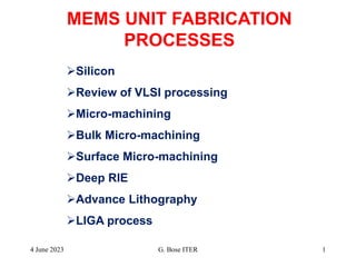
- 1. MEMS UNIT FABRICATION PROCESSES Silicon Review of VLSI processing Micro-machining Bulk Micro-machining Surface Micro-machining Deep RIE Advance Lithography LIGA process 4 June 2023 1 G. Bose ITER
- 2. SILICON WAFER FABRICATION Phase 1: Raw material and purification Quartzite Metallurgical Grade Si (MGS) Poly Si Process: Quartzite + Carbon (coal or coke) arc heating at 2000 °C : 2C (solid) + SiO2 (solid) Si (liquid) + 2CO Remains Fe + Al + 98% pure solid Si (MGS) Phase 2: MGS to EGS grade • Process: MGS (grinded) + gaseous HCl + catalyst • SiH4+SiH3Cl, SiH2Cl2,SiHCl3 and distillation • 2SiHCl3(gas) + 2H2 Si +6HCl • Poly Si rod is used as a seed Si. • Si contains 1013-1014 /cm3 ppb of impurities. 4 June 2023 2 G. Bose ITER
- 3. • MGS is charged in a crucible (graphite heater). • Pieces of MGS is heated 1417 ºC with small dopant. • Single crystal seed is then placed in the melt and pulled upward with rotates in one direction. CRYSTALLIZATION OF SILICON 1. Czocharalsky Method 4 June 2023 3 G. Bose ITER
- 4. 2. Floating zone method • No crucible is used. Hence very less impurity & defects. • Specially used for high resistivity Si wafer • Difficult to go for higher diameter of crystal due to mechanical stability problem and zone heating. • It has microscopic resistivity variation than the CZ • Conclusion: • CZ process is dominating till now 4 June 2023 4 G. Bose ITER
- 5. S IDENTIFICATION OF TYPE OF WAFER P Primary cut S Secondary cut P P 90° P 45° P S 180° (111) n-type (111) p-type (100) n-type (100) p-type 4 June 2023 5 G. Bose ITER
- 6. SILICON PROCESSING 4 June 2023 6 G. Bose ITER
- 7. Essential silicon wafer parameters Physical: Diameter Thickness Flatness Bow Mechanical defects Crystallographic defects Electrical: Type of dopant Resistivity Impurity (O2, C, Fe etc) 4 June 2023 7 G. Bose ITER
- 8. 4 June 2023 8 N2 O2 Gases Bubbler with heater Valves Pipes for water cooling Heating elements Quartz tubes Quartz tube supports Quartz boat Boat supports Wafers End cap Laminated & Filtered air Exhaust WAFER OXIDATION SYSTEM G. Bose ITER
- 9. 4 June 2023 9 OXIDATION Oxidation at high Temperature Si + O2 = SiO2 Si + H2O = SiO2 + 2H2 0.1 1 10 102 103 104 (t + τ)/ (A2/ 4B) 102 10 1 10-1 dox= B(t + τ) / A dox 2= B(t + τ) dox 2 + A do= B(t + τ) dox/ A2 G. Bose ITER
- 10. 4 June 2023 10 Photoresist After Spinning PHOTORESIST COATING A uniform layer of PR Before Spinning Wafer Vacuum Chuck Wafer holder G. Bose ITER
- 11. Final mask in matrix form 2nd Reduction by step and repeat camera, generally of “10 X” Reticle, after 1st reduction MASK GENERATION BY RETICLE OR 4 June 2023 11 G. Bose ITER
- 12. Oxidized silicon PR coated PR pattering Oxide film etching PR removed LITHOGRAPHY PROCESS STEPS Positive PR Negative PR
- 13. 4 June 2023 13 LIFT OFF TECHNIQUE PR coated on silicon Wafer to mask alignment Exposure Mask removal & pr development Metal deposition over pr Lift off G. Bose ITER
- 14. 4 June 2023 14 1. OPTICAL LITHOGRAPHY TECHNIQUES 1:1 Exposure systems Usually 4X, 5X or 10 X Reduction Contact Technique Proximity Technique Gap Light Lens Mask PR/Si Light Lens Projection Technique Mask PR/Si Light G. Bose ITER
- 15. 4 June 2023 15 Projection Mode Mask 2. X-RAY LITHOGRAPHY G. Bose ITER
- 16. 4 June 2023 16 MASK 1 FIRST MASK AND WAFER ALIGNMENT G. Bose ITER
- 17. 4 June 2023 17 PR DEVELOPMENT G. Bose ITER
- 18. 4 June 2023 18 OXIDE ETCHING Oxide etching Process •Load wafer in teflon jig •Dip into buffer Hydrofluoric (BHF) for 1 min. BHF: HF : NH4F: DI water 1 : 6 : 7 G. Bose ITER
- 19. DIRECTIONAL ETCHING Wet etching Anisotropic Dry etching Isotropic (Semi) Anisotropic 4 June 2023 19 G. Bose ITER
- 20. Isotropic etching Isotropic etching 4 June 2023 20 G. Bose ITER
- 21. 4 June 2023 21 PR REMOVAL Positive PR stripping •Dip in acetone till PR dissolves •Wash in DI water number of times. There are other number of other techniques are available. G. Bose ITER
- 22. 4 June 2023 22 Dopant diffusion followed by oxidation G. Bose ITER
- 23. )] Dt 2 x ( erf 1 [ 2 C ) t , x ( C ) Dt 4 x exp( ) t , 0 ( C ) Dt 4 x exp( Dt Q ) t , x ( C 2 2 “PRE-DEPOSITION”. "DRIVE – IN” 4 June 2023 23 G. Bose ITER
- 24. Normalized Concentration 10-2 10-1 0 1 2 3 4 1 10-3 5 Gaussian erfc X – units of √(Dt) SPATIAL FORM OF THE GAUSSIAN AND ERFC SOLUTIONS ARE SIMILAR FOR A PARTICULAR NORMALIZED VALUE OF Dt 4 June 2023 24 G. Bose ITER
- 25. 4 June 2023 25 N2 O2 Valves Pipes for water cooling Heating elements Quartz tubes Quartz tube supports Quartz boat Boat supports Wafers End cap Laminated Filtered air Exhaust Dopant Wafers WAFER DIFFUSION SYSTEM G. Bose ITER
- 26. 1 2 3 4 5 6 7 8 9 10 11 12 13 180KV + - + - Terminal ground ION-IMPLANTER 4 June 2023 26 G. Bose ITER
- 27. IONS DISTRIBUTION AT 200 KEV ENERGY 4 June 2023 27 G. Bose ITER
- 28. 4 June 2023 28 Contact mask: Lithography for contact, PR coat MASK – 2 Exposure through contact mask G. Bose ITER
- 29. 4 June 2023 29 Contact mask exposed PR development G. Bose ITER
- 30. 4 June 2023 30 PR Striping Metal deposition G. Bose ITER
- 31. INTRODUCTION FILM REQUIREMENT AND ISSUES 1. Qualities of films i.e. Composition, contamination, defects density, mechanical and electrical properties. 2. Uniformity. 3. Conformal step coverage. 4. Filling topographic structures, voids due to trapped chemicals and moisture etc. Aspect ratio (AR) = h/w oxide oxide oxide metal metal Metal h w h Metal Metal Poor feeling Poor step coverage 4 June 2023 31 Void G. Bose ITER
- 32. 4 June 2023 32 DIFFUSION PUMPED HIGH VACUUM EVAPORATION UNIT FILM MONITOR VACUUM Wafers in jig Roughing valve Baking valve High vacuum valve Chambe r Diff. pump Rotary pump N2 trap Heater Cooling coil Roughing Gauges Penning gauge 1. EVAPORATION TECHNIQUE PHYSICAL DEPOSITION TECHNIQUE G. Bose ITER
- 33. Electrode (target) Electrode Voltage + 0 VP V1 DistanceV2 Unequal area electrode (smaller electrode at left) Matching Network RF Source Electrode/target cathode) Electrode Wafers Heater Argon Plasma RF power input Sputtering gas inlet (Ar) Vacuum 4 June 2023 33 2. RF DEPOSITION TECHNIQUE G. Bose ITER
- 34. 4 June 2023 34 Metal patterning: Lithography, PR coat Metal mask alignment and light exposure G. Bose ITER
- 35. 4 June 2023 35 Previous step: Metal mask PR exposed PR development G. Bose ITER
- 36. 4 June 2023 36 ALUMINUM METAL ETCHING Phosphoric : Nitric : Acetic acid : Water 80 5 5 10 Some remarks: ø Etch rate = 2000 Å/ min at 25 c ø Room temperature, best 45 c ø Not very good edge definition as compare to dry. ø >2.5 micron is not advisable ø PR can be used as a mask. G. Bose ITER
- 37. 4 June 2023 37 Next Step: PR removal Previous step: Back metallization for contact & annealing G. Bose ITER
- 38. 4 June 2023 38 FABRICATED DIODE Back metal for electrical connection Front electrical for connection Silicon Diffused Dopant DIODE CROSS SECTION Back metal Oxide Metal Silicon Diffused dopant G. Bose ITER
- 39. MORE ABOUT DEPOSITION 4 June 2023 39 G. Bose ITER
- 40. Conformal deposition by sputtering system Lager arrival angle of atoms creates hangover, relatively no bottom and sides feeling and less reemission or diffusion Remedy: Arrival of atoms perpendicular to wafer surface by 1. Collimated sputter deposition through distance, 2. Collimated sputter deposition through holes, 2. RF antenna, 3. High-Temperature or Hot-Sputter deposition. 4 June 2023 40 G. Bose ITER
- 41. •Epi Si, is done by case2 to from single crystal (high temp) •SiO2 & Si3N4 is done by case1Low temp •Poly silicon is done by case1 Low temp Deposition Techniques 4 June 2023 41 G. Bose ITER
- 42. wafer susceptor 1 2 3 4 5 6 7 Gas stream Boundary layer Gas Silicon F1 CS F2 CG 1. Gas stream, 2. Diffusion of reactant from gas stream to wards wafer. 3. Adsorption of reactant on the wafer. 4. chemical decomposition or reaction and attached to proper sites. 5.Deaborption of byproduct. 6. Transport of byproduct into gas stream. 7. Transportation of byproduct out of rector. CVD PROCESS 4 June 2023 42 G. Bose ITER
- 43. Vent RF induction (heating) coils Quartz reaction chamber HCl H2+B2H6 H2+PH3 Ar H2 SiCl4 (liquid) H2 Si Wafers Graphite Susceptor APCVD EQUIPMENT 4 June 2023 43 G. Bose ITER
- 44. Vacuum pump Gas Control and Sequencer Source Gases Furnace – with resistance heaters Standup wafers Trap Exhaust scrubber LPCVD 4 June 2023 44 G. Bose ITER