Continuous Low Pass Filter Realization using Cascaded stages of Tow-Thomas Bi-quads
•
0 gefällt mir•402 views

Designed a Continuous Low Pass Filter using three stages of cascaded Tow-Thomas Bi-quads which met the following specifications:- Pass band: DC to fp = 20 kHz, gain between 0 dB & 1 dB. Stop band: f > fs = 40 kHz, gain below -50 dB Found the transfer function, poles and zeros of the required filter using MATLAB. Used Cadence to plot the frequency response of the gain of the overall transfer function using ideal op-amps and non-ideal op-amps.Used dynamic optimization and dynamic range scaling of the elements (resistors and capacitors) such that the output of each stage had a good output swing.

Empfohlen
Empfohlen
Weitere ähnliche Inhalte
Was ist angesagt?
Was ist angesagt? (20)
Andere mochten auch
Andere mochten auch (7)
Ähnlich wie Continuous Low Pass Filter Realization using Cascaded stages of Tow-Thomas Bi-quads
Ähnlich wie Continuous Low Pass Filter Realization using Cascaded stages of Tow-Thomas Bi-quads (20)
Mehr von Karthik Rathinavel
Mehr von Karthik Rathinavel (8)
Kürzlich hochgeladen
Kürzlich hochgeladen (20)
Continuous Low Pass Filter Realization using Cascaded stages of Tow-Thomas Bi-quads
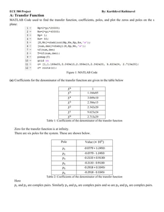
- 1. ECE 580 Project By: Karthikvel Rathinavel A: Transfer Function MATLAB Code used to find the transfer function, coefficients, poles, and plot the zeros and poles on the s plane: Figure 1: MATLAB Code (a) Coefficients for the denominator of the transfer function are given in the table below 1 1.166e05 3.049e10 2.386e15 2.342e20 9.623e24 2.713e29 Table 1: Coefficients of the denominator of the transfer function Zero for the transfer function is at infinity. There are six poles for the system. These are shown below. Pole Value ( 10 ‐0.0779 + 1.2492i ‐0.0779 ‐ 1.2492i ‐0.2133 + 0.9130i ‐0.2133 ‐ 0.9130i ‐0.2918 + 0.3345i ‐0.2918 ‐ 0.3345i Table 2: Coefficients of the denominator of the transfer function Here and are complex pairs. Similarly and are complex pairs and so are and are complex pairs.
- 2. (b) All the six poles can be plotted in the s plane which are lying in the left half of the plane. This is shown in figure 1. Figure 2: Location of poles Here note that zeros are at infinity Figure 3: Location of poles with grid on
- 3. (c) The transfer function after simplification is given: 2.4184 10 15580 1.56606941 10 42660 0.87906589 10 58340 0.19657125 10 Here we factored the all three complex conjugate pole pairs so that the resultant transfer function only has real coefficients. It can be also done by using the command; zpk (T) where the T represents the transfer function. (d) The phase and gain are plotted by varying frequency from 0 150 and by plotting it against gain (logarithmic scale) and phase. Thus we can obtain the following two graphs. Figure 4: Gain and Phase plot for the frequencies ranging from 0 150
- 4. B: Realization of transfer function For the realization of the transfer function first we treat each factor (second order in s) as one transfer function. Each transfer function can now be treated as a Tow-Thomas Bi-quad. The values for all the circuit elements for the initial circuit design, can be found by individually comparing the coefficients of each segment of the transfer function. After making sure that the high Q is in the middle. All three Tow- Bi-quads were cascaded to get the overall initial design of the low pass filter. (a) Final circuit diagram and element values: Figure 5: Schematic of Final Circuit Final element values are given for each stage are given below in the table below Element value (s) (s) C 1.034703971 uF 728.1199942 nF 241.7561164 nF C 1 uF 1 uF 1u F R 62.03126864 ohms 17.06797728 ohms 70.897896 ohms R 7.9908 ohms 10.665698 ohms 22.5548 ohms R 32.1376 ohms 16.18672 ohms 4.135 ohms R 7.9908 ohms 10.665698 ohms 22.5548 ohms R 1 K ohms 1 K ohms 1 K ohms These final values are found by first performing dynamic range optimization and dynamic range scaling followed by dynamic range scaling for the first integrator of each stage, in the initial design. Finally all the impedances connected to the input were scaled so that area on chip can be minimized and lower noise. Initial element values used for the initial design are given in the table below Element value (s) (s) C 1uF 1 uF 1 uF C 1 uF 1 uF 1u F R 64.1848 u ohms 23.4416 u ohms 17.14 u ohms R 7.9908 u ohms 10.665698 u ohms 22.5548 u ohms R 20.086 u ohms 15.0487 u ohms 7.11634 u ohms R 7.9908 u ohms 10.665698 u ohms 22.5548 u ohms R 2 K ohms 2 K ohms 2 K ohms
- 5. (b) Scaled element values so that maximum output voltage of all active blocks are equal Since each stage is a linear block, multiplying each individual stage by a certain factor will not have any impact on the overall transfer function as long as the overall constants multiply to give 1. This process of multiplying each stage by a factor ‘k’ such that the maximum output voltage of each block remains same is called dynamic range optimization. First the voltage gain was observed for the first stage and then this gain was scaled by multiplying it to the input resistance ( ) this ensures that gain of the first stage is 1 (0 dB), because is inversely proportional to the transfer function of the block. This process is repeated for the second block such that the output gain between the input and the output of the second block remains the same. Now since we have introduced an additional two constants (say and ) we then scale the final stage with a constant such that 1. In this project the scaling factors were found to be:- 1.6 1.07562 1 0.58106 These scaling factors ensured that the maximum output of each stage remained the same. Thus ensuring we get maximum output swing in the linear range of the op-amp. Figure 6: Gain curve for each stage after performing dynamic range optimization Here the three transfer functions were cascaded with each other. It can be seen in figure 6, that the peaks of each of the individual transfer function lie under 0 dB.
- 6. (c) Simulating circuit before and after scaling The gain plots for each stage of the transfer function is plotted before scaling and after scaling. (i) Before scaling or initial design Figure 7: Schematic for Initial Design Figure 8: Gain vs Frequency plot for the initial design for each transfer function Before scaling, it can be observed that the first two transfer functions of the first two Bi-quads are peaking at a higher value and are not confined to 0 dB. It can be seen in the figure above (Figure 6), it is approximately 4.8 dB higher than 0 dB. Now we can find the scaling factor for each of the transfer function such that at each stage it is confined to 0 dB. Since each transfer function is a linear block, multiplying by a factor ‘k’ will result in the output voltage to increase by the same factor.
- 7. (ii) After scaling in order to get maximum output voltages Figure 9: Schematic after performing dynamic range optimization Figure 10: Gain vs Frequency plot after performing dynamic range optimization Note that after doing dynamic range optimization, the maximum output gain of each stage is under 0 dB. Next we scale the impedances connected to each of the integrators of the three stages. This is done by following the same process for dynamic range optimization except we observe the voltage gain of each of the integrators (first op-amp) of each stage separately.
- 8. (iii) Dynamic scaling for each integrators (first op-amp of each block) Figure 11: Schematic after performing dynamic range scaling of the integrators Figure 12: Final Gain vs Frequency plot after performing dynamic range optimization (iv) Impedance scaling Finally impedance scaling was done to account for lower noise. A scaling factor was found such that all the impedance connected to the input node was scaled without changing the output voltage. Since there were no capacitors connected to the input, they were not altered to lower chip area. The gain plot looked exactly the same as before, upon performing impedance scaling.
- 9. (d) Simulations before and after scaling for non-ideal op-amp In addition to adding a parasitic capacitance (few femto farads), the op-amp with very high gain (around 80 dB) op-amp was replaced with a non-ideal op-amp (with finite gain) to observe the non-ideal behavior. Figure 13: Schematic for observing the effects of non-ideal behavior in op-amps (i) Before scaling non ideal op-amp with parasitic capacitance Figure 14: Gain vs Frequency plot for non-ideal op-amp before scaling
- 10. (ii) After scaling non ideal op-amp Figure 15: Gain vs Frequency plot for non-ideal op-amp after scaling Minimizing non-ideal effects: It can be observed from the figure above that the passband gain after scaling for non-ideal op-amp becomes well below -1 dB and it is no longer in the required range of 0 to -1 dB. One way of minimizing these effects is to use lower width of the transistor (MOSFETs) inside the op-amp such that the parasitic capacitance is reduced. However this comes at the cost of reducing the overall gain of the op-amp. Another way to increase the gain of op-amps is to cascade multiple stages of operation inside each op-amp. This will increase the gain of each op-amp so that it approaches ideal behavior.