SlideShare ist ein Scribd-Unternehmen logo
1 von 18
PRINTED BOARD CIRCUIT DESIGN
(PCB)
PRABHANJAN KUMAR
&
Kumar gautam
CONTENT
1. INTRODUCTION
2. TYPES OF PCB
3. PCB TERMINOLOGY
4. PCB FLOW
5. PLACEMENT RULES
6. INTRODUCTION TO DESIGN RULE
7. FABRICATED PCB BOARD
8. SUMMARY
INTRODUCTION
➢ Printed circuit board can be shortly
called PCB.
➢ PCB were first developed by an
australian engineer Paul Eisler.
➢ PCB is a non conductive substrate
that mechanically support and
electrical connects the electronic
components using track pads and
other features etched on a laminated
copper sheet.
TYPES OF PCB
There are mainly three types of PCBs
1. Single-sided PCB----- Component placement/Routing only on
one side (TOP/BOTTOM)
2. Double-sided PCB--- Component placement/Routing only on
both side (TOP & BOTTOM)
3. Multilayer PCB----Component placement on both side and
Routing also internal layers.
PRINTED CIRCUIT BOARD TERMINOLOGY
1. Bare board : This term refers to a circuit board with no
components mounted on it.
2. Trace : This term refers to the copper width of the PCB wires.
3. Via : Interconnection of signal between different layers of a
PCB.
4. Pad : This is one of the most basic units of PCB. A pad is a
contact point used to connect components with a via and is the
point to which the components are soldered.
PCB FLOW
LIBRARY CREATION OF COMPONENTS IN
ORCAD
● We have to create each and every component in library.
PCB DESIGNING PROCESS
Step by step:
● Schematic design: It is a circuit diagram. It uses agreed
symbols to represent components and show how they
area electrically connected.
ENTERING PCB FOOTPRINT FILE & CREATE
NETLIST
COMPONENT PLACEMENT
ROUTING & LENGTH MATCHING
● In electronic design, wire routing, commonly called
simply routing, is a step in the design of printed circuit
board and integrated circuit.
GERBER FILE
● The gerber format is an open ASCII vector format for 2D
binary image. It is used to describe the printed circuit board
images: copper layer solder mask.
POST FABRICATION
● The gerber format is loaded to different machine (Re-flow
Soldering/Wave Soldering Machine) to fabricate the final
physical PCB board.
Ten Rules for Components Placement on PCB Design
1. Start placement of big/main/critical components( this could be
MCU,DSP,FPGA,DDR, clock devices) and then place support component like
resistors, capacitors around them.
2. Use 50 or 100mil as component grid to place these big components ( QFP, BGA,
SOP, SOIC, or through hole connectors). Use 25mil as component gird for these SMT
resistors/capacitors or other small passive components.
3. Isolate the analog, digital and power supply section.
4. Clock driver/synchronizer should be located close to clock oscillator.
5. Arrange components in rows and columns, and oriented uniformly for ease of
installation, inspection and rework. When possible, all polarized components such as
tantrum capacitor and diodes in the same direction. Polarity of these components
should be indicated on the silkscreen.
6. Keep at least 40mil space between components and 100mil space from component
to board edge. Locate connectors on one edge or one corner of the board.
7. Try to place all components on the top side only. If not possible, only these low
profile, small size and low thermal dissipation component (like SMD passive parts) can
be on bottom side.
8. Place decoupling capacitors close as much as possible to VCC pin on active
components.
9. Keep at least 200mil clearance from transformer to electrolytic capacitor.
10. Locate indication LEDs, test points, switches, jumpers and adjustable components
for easy access.
One more rule, it’s always good to double check analog, high frequency, RF, high
voltage, high profile, heavy or high heat components before starting trace routing.
Introduction to Design Rules
● There are four types of design rules:
- Electrical Constraints: Performance characteristics
- Physical Constraints: Line (Trace) width, via selection, and
layer restriction
- Spacing Constraints: Clearances between lines,pads,
vias,and copper
- Same Net Spacing constraints: Clearances between lines
pads vias, and copper areas (shape) on the same net.These
are differentiated From Net to Net rules from Net to net rules
SUMMARY
➢ PCB were first developed by an Australian engineer Paul
Eisler.
➢ Mainly 3 types of PCB.
➢ Schematic, Footprint creation, Placement, Routing are basic
steps of PCB’s.
➢ Analysis ensures signal to be recieved with proper strength.
➢ Gerber file is used for fabrication and assembly process.
QUESTIONS???
Thank you

Weitere ähnliche Inhalte

Was ist angesagt?

Designing process of printed circuit boards
Designing process of printed circuit boardsDesigning process of printed circuit boards
Designing process of printed circuit boardselprocus
 
PPT ON PCB DESIGN INTERNSHIP
PPT ON PCB DESIGN INTERNSHIPPPT ON PCB DESIGN INTERNSHIP
PPT ON PCB DESIGN INTERNSHIPSujoyHalder4
 
Surface mount Devices(SMD)
Surface mount Devices(SMD)Surface mount Devices(SMD)
Surface mount Devices(SMD)shyamaliamale
 
Printed circuit Board Description
Printed circuit Board DescriptionPrinted circuit Board Description
Printed circuit Board DescriptionRUBY DIKSHIT
 
PCB designing and Manufacturing
PCB designing and Manufacturing PCB designing and Manufacturing
PCB designing and Manufacturing ManishKenchi
 
Design of Printed Circuit Boards
Design of Printed Circuit BoardsDesign of Printed Circuit Boards
Design of Printed Circuit BoardsChandana129742
 
Introduction to Surface Mount Technology
Introduction to Surface Mount TechnologyIntroduction to Surface Mount Technology
Introduction to Surface Mount TechnologyABDUL MUNAFF
 
Introduction to PCB Design
Introduction to PCB DesignIntroduction to PCB Design
Introduction to PCB DesignSharan kumar
 
Printed circuit board
Printed circuit boardPrinted circuit board
Printed circuit boardSuhail Ahmed
 
Low power vlsi design ppt
Low power vlsi design pptLow power vlsi design ppt
Low power vlsi design pptAnil Yadav
 
Presentation on Scaling
Presentation on ScalingPresentation on Scaling
Presentation on ScalingRaviraj Kaur
 
Report on PCB designing and fabrication by Prince Rohan
Report on PCB designing and fabrication by Prince RohanReport on PCB designing and fabrication by Prince Rohan
Report on PCB designing and fabrication by Prince RohanRohan Das
 

Was ist angesagt? (20)

Designing process of printed circuit boards
Designing process of printed circuit boardsDesigning process of printed circuit boards
Designing process of printed circuit boards
 
PPT ON PCB DESIGN INTERNSHIP
PPT ON PCB DESIGN INTERNSHIPPPT ON PCB DESIGN INTERNSHIP
PPT ON PCB DESIGN INTERNSHIP
 
pcb
pcbpcb
pcb
 
Surface mount Devices(SMD)
Surface mount Devices(SMD)Surface mount Devices(SMD)
Surface mount Devices(SMD)
 
Printed circuit Board Description
Printed circuit Board DescriptionPrinted circuit Board Description
Printed circuit Board Description
 
PCB Designing
PCB Designing PCB Designing
PCB Designing
 
PCB designing and Manufacturing
PCB designing and Manufacturing PCB designing and Manufacturing
PCB designing and Manufacturing
 
WelcomePCB
WelcomePCBWelcomePCB
WelcomePCB
 
Pcb design powerpoint
Pcb design powerpointPcb design powerpoint
Pcb design powerpoint
 
Design of Printed Circuit Boards
Design of Printed Circuit BoardsDesign of Printed Circuit Boards
Design of Printed Circuit Boards
 
INTRODUCTION TO PCB
INTRODUCTION TO PCBINTRODUCTION TO PCB
INTRODUCTION TO PCB
 
Introduction to Surface Mount Technology
Introduction to Surface Mount TechnologyIntroduction to Surface Mount Technology
Introduction to Surface Mount Technology
 
Introduction to PCB Design
Introduction to PCB DesignIntroduction to PCB Design
Introduction to PCB Design
 
Printed circuit board
Printed circuit boardPrinted circuit board
Printed circuit board
 
PCB Layout Fundamentals
PCB Layout FundamentalsPCB Layout Fundamentals
PCB Layout Fundamentals
 
Short Channel Effect In MOSFET
Short Channel Effect In MOSFETShort Channel Effect In MOSFET
Short Channel Effect In MOSFET
 
Low power vlsi design ppt
Low power vlsi design pptLow power vlsi design ppt
Low power vlsi design ppt
 
BiCMOS Technology
BiCMOS TechnologyBiCMOS Technology
BiCMOS Technology
 
Presentation on Scaling
Presentation on ScalingPresentation on Scaling
Presentation on Scaling
 
Report on PCB designing and fabrication by Prince Rohan
Report on PCB designing and fabrication by Prince RohanReport on PCB designing and fabrication by Prince Rohan
Report on PCB designing and fabrication by Prince Rohan
 

Ähnlich wie Printed board circuit design (Pcb) PPT

Pcb design using_eagle
Pcb design using_eaglePcb design using_eagle
Pcb design using_eagleABDUL MUNAFF
 
Electronic circuit design and component selection.pptx
Electronic circuit design and component selection.pptxElectronic circuit design and component selection.pptx
Electronic circuit design and component selection.pptxmaheshmp16
 
Surface mount technology (smt) and smd packages
Surface mount technology (smt) and smd packagesSurface mount technology (smt) and smd packages
Surface mount technology (smt) and smd packageskaren zou
 
Pcbdesign 140510145153-phpapp01
Pcbdesign 140510145153-phpapp01Pcbdesign 140510145153-phpapp01
Pcbdesign 140510145153-phpapp01ssantosh1234
 
PCB Terminologies in PCB designing
PCB Terminologies in PCB designingPCB Terminologies in PCB designing
PCB Terminologies in PCB designingMSHOAIBASLAM1
 
PCB Fabrication, China PCB Circuit Board Manufacturing from China
PCB Fabrication, China PCB Circuit Board Manufacturing from ChinaPCB Fabrication, China PCB Circuit Board Manufacturing from China
PCB Fabrication, China PCB Circuit Board Manufacturing from ChinaLeah-Hitech PCB
 
Learning outcome 2 prepare make pcb modules
Learning outcome 2 prepare make pcb modulesLearning outcome 2 prepare make pcb modules
Learning outcome 2 prepare make pcb modulesAr Kyu Dee
 
Importance of PCB assembly in Various Industries | Suntronic Inc |
Importance of PCB assembly in Various Industries | Suntronic Inc |Importance of PCB assembly in Various Industries | Suntronic Inc |
Importance of PCB assembly in Various Industries | Suntronic Inc |SuntronicInc
 
Chapter12 manufacturing-processes
Chapter12 manufacturing-processesChapter12 manufacturing-processes
Chapter12 manufacturing-processesVin Voro
 
presentation1-131031235854-phpapp02.pptx
presentation1-131031235854-phpapp02.pptxpresentation1-131031235854-phpapp02.pptx
presentation1-131031235854-phpapp02.pptxSirachartChuto
 
Printed Circuit Board Design Techniques for EMC Compliance_20240220_145105_00...
Printed Circuit Board Design Techniques for EMC Compliance_20240220_145105_00...Printed Circuit Board Design Techniques for EMC Compliance_20240220_145105_00...
Printed Circuit Board Design Techniques for EMC Compliance_20240220_145105_00...AlanGustavo13
 

Ähnlich wie Printed board circuit design (Pcb) PPT (20)

Pcb design using_eagle
Pcb design using_eaglePcb design using_eagle
Pcb design using_eagle
 
PCB fabrication.pptx
PCB fabrication.pptxPCB fabrication.pptx
PCB fabrication.pptx
 
Electronic circuit design and component selection.pptx
Electronic circuit design and component selection.pptxElectronic circuit design and component selection.pptx
Electronic circuit design and component selection.pptx
 
ACHAL NEET PPT OF PCB-1.pptx
ACHAL NEET PPT OF PCB-1.pptxACHAL NEET PPT OF PCB-1.pptx
ACHAL NEET PPT OF PCB-1.pptx
 
Pcb layout
Pcb layoutPcb layout
Pcb layout
 
Surface mount technology (smt) and smd packages
Surface mount technology (smt) and smd packagesSurface mount technology (smt) and smd packages
Surface mount technology (smt) and smd packages
 
PCB
PCBPCB
PCB
 
PCB desine final.pdf
PCB desine final.pdfPCB desine final.pdf
PCB desine final.pdf
 
Pcbdesign 140510145153-phpapp01
Pcbdesign 140510145153-phpapp01Pcbdesign 140510145153-phpapp01
Pcbdesign 140510145153-phpapp01
 
Pcb design
Pcb designPcb design
Pcb design
 
Pcb design
Pcb designPcb design
Pcb design
 
PCB Terminologies in PCB designing
PCB Terminologies in PCB designingPCB Terminologies in PCB designing
PCB Terminologies in PCB designing
 
PCB Fabrication, China PCB Circuit Board Manufacturing from China
PCB Fabrication, China PCB Circuit Board Manufacturing from ChinaPCB Fabrication, China PCB Circuit Board Manufacturing from China
PCB Fabrication, China PCB Circuit Board Manufacturing from China
 
PCB Assembly Manufacturer Hitech circuits
PCB Assembly Manufacturer Hitech circuitsPCB Assembly Manufacturer Hitech circuits
PCB Assembly Manufacturer Hitech circuits
 
Learning outcome 2 prepare make pcb modules
Learning outcome 2 prepare make pcb modulesLearning outcome 2 prepare make pcb modules
Learning outcome 2 prepare make pcb modules
 
Importance of PCB assembly in Various Industries | Suntronic Inc |
Importance of PCB assembly in Various Industries | Suntronic Inc |Importance of PCB assembly in Various Industries | Suntronic Inc |
Importance of PCB assembly in Various Industries | Suntronic Inc |
 
Chapter12 manufacturing-processes
Chapter12 manufacturing-processesChapter12 manufacturing-processes
Chapter12 manufacturing-processes
 
presentation1-131031235854-phpapp02.pptx
presentation1-131031235854-phpapp02.pptxpresentation1-131031235854-phpapp02.pptx
presentation1-131031235854-phpapp02.pptx
 
Printed Circuit Board Design Techniques for EMC Compliance_20240220_145105_00...
Printed Circuit Board Design Techniques for EMC Compliance_20240220_145105_00...Printed Circuit Board Design Techniques for EMC Compliance_20240220_145105_00...
Printed Circuit Board Design Techniques for EMC Compliance_20240220_145105_00...
 
Jsk urja pcb ppt
Jsk urja pcb pptJsk urja pcb ppt
Jsk urja pcb ppt
 

Kürzlich hochgeladen

University management System project report..pdf
University management System project report..pdfUniversity management System project report..pdf
University management System project report..pdfKamal Acharya
 
VIP Call Girls Palanpur 7001035870 Whatsapp Number, 24/07 Booking
VIP Call Girls Palanpur 7001035870 Whatsapp Number, 24/07 BookingVIP Call Girls Palanpur 7001035870 Whatsapp Number, 24/07 Booking
VIP Call Girls Palanpur 7001035870 Whatsapp Number, 24/07 Bookingdharasingh5698
 
ONLINE FOOD ORDER SYSTEM PROJECT REPORT.pdf
ONLINE FOOD ORDER SYSTEM PROJECT REPORT.pdfONLINE FOOD ORDER SYSTEM PROJECT REPORT.pdf
ONLINE FOOD ORDER SYSTEM PROJECT REPORT.pdfKamal Acharya
 
XXXXXXXXXXXXXXXXXXXXXXXXXXXXXXXXXXXXXXXXXXXXXXXXXXXX
XXXXXXXXXXXXXXXXXXXXXXXXXXXXXXXXXXXXXXXXXXXXXXXXXXXXXXXXXXXXXXXXXXXXXXXXXXXXXXXXXXXXXXXXXXXXXXXXXXXXXXXX
XXXXXXXXXXXXXXXXXXXXXXXXXXXXXXXXXXXXXXXXXXXXXXXXXXXXssuser89054b
 
chapter 5.pptx: drainage and irrigation engineering
chapter 5.pptx: drainage and irrigation engineeringchapter 5.pptx: drainage and irrigation engineering
chapter 5.pptx: drainage and irrigation engineeringmulugeta48
 
Call Girls In Bangalore ☎ 7737669865 🥵 Book Your One night Stand
Call Girls In Bangalore ☎ 7737669865 🥵 Book Your One night StandCall Girls In Bangalore ☎ 7737669865 🥵 Book Your One night Stand
Call Girls In Bangalore ☎ 7737669865 🥵 Book Your One night Standamitlee9823
 
Thermal Engineering -unit - III & IV.ppt
Thermal Engineering -unit - III & IV.pptThermal Engineering -unit - III & IV.ppt
Thermal Engineering -unit - III & IV.pptDineshKumar4165
 
Thermal Engineering Unit - I & II . ppt
Thermal Engineering  Unit - I & II . pptThermal Engineering  Unit - I & II . ppt
Thermal Engineering Unit - I & II . pptDineshKumar4165
 
Design For Accessibility: Getting it right from the start
Design For Accessibility: Getting it right from the startDesign For Accessibility: Getting it right from the start
Design For Accessibility: Getting it right from the startQuintin Balsdon
 
Thermal Engineering-R & A / C - unit - V
Thermal Engineering-R & A / C - unit - VThermal Engineering-R & A / C - unit - V
Thermal Engineering-R & A / C - unit - VDineshKumar4165
 
Bhosari ( Call Girls ) Pune 6297143586 Hot Model With Sexy Bhabi Ready For ...
Bhosari ( Call Girls ) Pune  6297143586  Hot Model With Sexy Bhabi Ready For ...Bhosari ( Call Girls ) Pune  6297143586  Hot Model With Sexy Bhabi Ready For ...
Bhosari ( Call Girls ) Pune 6297143586 Hot Model With Sexy Bhabi Ready For ...tanu pandey
 
Intro To Electric Vehicles PDF Notes.pdf
Intro To Electric Vehicles PDF Notes.pdfIntro To Electric Vehicles PDF Notes.pdf
Intro To Electric Vehicles PDF Notes.pdfrs7054576148
 
CCS335 _ Neural Networks and Deep Learning Laboratory_Lab Complete Record
CCS335 _ Neural Networks and Deep Learning Laboratory_Lab Complete RecordCCS335 _ Neural Networks and Deep Learning Laboratory_Lab Complete Record
CCS335 _ Neural Networks and Deep Learning Laboratory_Lab Complete RecordAsst.prof M.Gokilavani
 
Block diagram reduction techniques in control systems.ppt
Block diagram reduction techniques in control systems.pptBlock diagram reduction techniques in control systems.ppt
Block diagram reduction techniques in control systems.pptNANDHAKUMARA10
 
Call Girls Pimpri Chinchwad Call Me 7737669865 Budget Friendly No Advance Boo...
Call Girls Pimpri Chinchwad Call Me 7737669865 Budget Friendly No Advance Boo...Call Girls Pimpri Chinchwad Call Me 7737669865 Budget Friendly No Advance Boo...
Call Girls Pimpri Chinchwad Call Me 7737669865 Budget Friendly No Advance Boo...roncy bisnoi
 

Kürzlich hochgeladen (20)

University management System project report..pdf
University management System project report..pdfUniversity management System project report..pdf
University management System project report..pdf
 
VIP Call Girls Palanpur 7001035870 Whatsapp Number, 24/07 Booking
VIP Call Girls Palanpur 7001035870 Whatsapp Number, 24/07 BookingVIP Call Girls Palanpur 7001035870 Whatsapp Number, 24/07 Booking
VIP Call Girls Palanpur 7001035870 Whatsapp Number, 24/07 Booking
 
(INDIRA) Call Girl Meerut Call Now 8617697112 Meerut Escorts 24x7
(INDIRA) Call Girl Meerut Call Now 8617697112 Meerut Escorts 24x7(INDIRA) Call Girl Meerut Call Now 8617697112 Meerut Escorts 24x7
(INDIRA) Call Girl Meerut Call Now 8617697112 Meerut Escorts 24x7
 
ONLINE FOOD ORDER SYSTEM PROJECT REPORT.pdf
ONLINE FOOD ORDER SYSTEM PROJECT REPORT.pdfONLINE FOOD ORDER SYSTEM PROJECT REPORT.pdf
ONLINE FOOD ORDER SYSTEM PROJECT REPORT.pdf
 
FEA Based Level 3 Assessment of Deformed Tanks with Fluid Induced Loads
FEA Based Level 3 Assessment of Deformed Tanks with Fluid Induced LoadsFEA Based Level 3 Assessment of Deformed Tanks with Fluid Induced Loads
FEA Based Level 3 Assessment of Deformed Tanks with Fluid Induced Loads
 
XXXXXXXXXXXXXXXXXXXXXXXXXXXXXXXXXXXXXXXXXXXXXXXXXXXX
XXXXXXXXXXXXXXXXXXXXXXXXXXXXXXXXXXXXXXXXXXXXXXXXXXXXXXXXXXXXXXXXXXXXXXXXXXXXXXXXXXXXXXXXXXXXXXXXXXXXXXXX
XXXXXXXXXXXXXXXXXXXXXXXXXXXXXXXXXXXXXXXXXXXXXXXXXXXX
 
chapter 5.pptx: drainage and irrigation engineering
chapter 5.pptx: drainage and irrigation engineeringchapter 5.pptx: drainage and irrigation engineering
chapter 5.pptx: drainage and irrigation engineering
 
Call Girls In Bangalore ☎ 7737669865 🥵 Book Your One night Stand
Call Girls In Bangalore ☎ 7737669865 🥵 Book Your One night StandCall Girls In Bangalore ☎ 7737669865 🥵 Book Your One night Stand
Call Girls In Bangalore ☎ 7737669865 🥵 Book Your One night Stand
 
Call Now ≽ 9953056974 ≼🔝 Call Girls In New Ashok Nagar ≼🔝 Delhi door step de...
Call Now ≽ 9953056974 ≼🔝 Call Girls In New Ashok Nagar  ≼🔝 Delhi door step de...Call Now ≽ 9953056974 ≼🔝 Call Girls In New Ashok Nagar  ≼🔝 Delhi door step de...
Call Now ≽ 9953056974 ≼🔝 Call Girls In New Ashok Nagar ≼🔝 Delhi door step de...
 
Thermal Engineering -unit - III & IV.ppt
Thermal Engineering -unit - III & IV.pptThermal Engineering -unit - III & IV.ppt
Thermal Engineering -unit - III & IV.ppt
 
Thermal Engineering Unit - I & II . ppt
Thermal Engineering  Unit - I & II . pptThermal Engineering  Unit - I & II . ppt
Thermal Engineering Unit - I & II . ppt
 
Call Girls in Ramesh Nagar Delhi 💯 Call Us 🔝9953056974 🔝 Escort Service
Call Girls in Ramesh Nagar Delhi 💯 Call Us 🔝9953056974 🔝 Escort ServiceCall Girls in Ramesh Nagar Delhi 💯 Call Us 🔝9953056974 🔝 Escort Service
Call Girls in Ramesh Nagar Delhi 💯 Call Us 🔝9953056974 🔝 Escort Service
 
Design For Accessibility: Getting it right from the start
Design For Accessibility: Getting it right from the startDesign For Accessibility: Getting it right from the start
Design For Accessibility: Getting it right from the start
 
Water Industry Process Automation & Control Monthly - April 2024
Water Industry Process Automation & Control Monthly - April 2024Water Industry Process Automation & Control Monthly - April 2024
Water Industry Process Automation & Control Monthly - April 2024
 
Thermal Engineering-R & A / C - unit - V
Thermal Engineering-R & A / C - unit - VThermal Engineering-R & A / C - unit - V
Thermal Engineering-R & A / C - unit - V
 
Bhosari ( Call Girls ) Pune 6297143586 Hot Model With Sexy Bhabi Ready For ...
Bhosari ( Call Girls ) Pune  6297143586  Hot Model With Sexy Bhabi Ready For ...Bhosari ( Call Girls ) Pune  6297143586  Hot Model With Sexy Bhabi Ready For ...
Bhosari ( Call Girls ) Pune 6297143586 Hot Model With Sexy Bhabi Ready For ...
 
Intro To Electric Vehicles PDF Notes.pdf
Intro To Electric Vehicles PDF Notes.pdfIntro To Electric Vehicles PDF Notes.pdf
Intro To Electric Vehicles PDF Notes.pdf
 
CCS335 _ Neural Networks and Deep Learning Laboratory_Lab Complete Record
CCS335 _ Neural Networks and Deep Learning Laboratory_Lab Complete RecordCCS335 _ Neural Networks and Deep Learning Laboratory_Lab Complete Record
CCS335 _ Neural Networks and Deep Learning Laboratory_Lab Complete Record
 
Block diagram reduction techniques in control systems.ppt
Block diagram reduction techniques in control systems.pptBlock diagram reduction techniques in control systems.ppt
Block diagram reduction techniques in control systems.ppt
 
Call Girls Pimpri Chinchwad Call Me 7737669865 Budget Friendly No Advance Boo...
Call Girls Pimpri Chinchwad Call Me 7737669865 Budget Friendly No Advance Boo...Call Girls Pimpri Chinchwad Call Me 7737669865 Budget Friendly No Advance Boo...
Call Girls Pimpri Chinchwad Call Me 7737669865 Budget Friendly No Advance Boo...
 

Printed board circuit design (Pcb) PPT

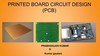
  • 1. PRINTED BOARD CIRCUIT DESIGN (PCB) PRABHANJAN KUMAR & Kumar gautam
  • 2. CONTENT 1. INTRODUCTION 2. TYPES OF PCB 3. PCB TERMINOLOGY 4. PCB FLOW 5. PLACEMENT RULES 6. INTRODUCTION TO DESIGN RULE 7. FABRICATED PCB BOARD 8. SUMMARY
  • 3. INTRODUCTION ➢ Printed circuit board can be shortly called PCB. ➢ PCB were first developed by an australian engineer Paul Eisler. ➢ PCB is a non conductive substrate that mechanically support and electrical connects the electronic components using track pads and other features etched on a laminated copper sheet.
  • 4. TYPES OF PCB There are mainly three types of PCBs 1. Single-sided PCB----- Component placement/Routing only on one side (TOP/BOTTOM) 2. Double-sided PCB--- Component placement/Routing only on both side (TOP & BOTTOM) 3. Multilayer PCB----Component placement on both side and Routing also internal layers.
  • 5. PRINTED CIRCUIT BOARD TERMINOLOGY 1. Bare board : This term refers to a circuit board with no components mounted on it. 2. Trace : This term refers to the copper width of the PCB wires. 3. Via : Interconnection of signal between different layers of a PCB. 4. Pad : This is one of the most basic units of PCB. A pad is a contact point used to connect components with a via and is the point to which the components are soldered.
  • 7. LIBRARY CREATION OF COMPONENTS IN ORCAD ● We have to create each and every component in library.
  • 8. PCB DESIGNING PROCESS Step by step: ● Schematic design: It is a circuit diagram. It uses agreed symbols to represent components and show how they area electrically connected.
  • 9. ENTERING PCB FOOTPRINT FILE & CREATE NETLIST
  • 11. ROUTING & LENGTH MATCHING ● In electronic design, wire routing, commonly called simply routing, is a step in the design of printed circuit board and integrated circuit.
  • 12. GERBER FILE ● The gerber format is an open ASCII vector format for 2D binary image. It is used to describe the printed circuit board images: copper layer solder mask.
  • 13. POST FABRICATION ● The gerber format is loaded to different machine (Re-flow Soldering/Wave Soldering Machine) to fabricate the final physical PCB board.
  • 14. Ten Rules for Components Placement on PCB Design 1. Start placement of big/main/critical components( this could be MCU,DSP,FPGA,DDR, clock devices) and then place support component like resistors, capacitors around them. 2. Use 50 or 100mil as component grid to place these big components ( QFP, BGA, SOP, SOIC, or through hole connectors). Use 25mil as component gird for these SMT resistors/capacitors or other small passive components. 3. Isolate the analog, digital and power supply section. 4. Clock driver/synchronizer should be located close to clock oscillator. 5. Arrange components in rows and columns, and oriented uniformly for ease of installation, inspection and rework. When possible, all polarized components such as tantrum capacitor and diodes in the same direction. Polarity of these components should be indicated on the silkscreen.
  • 15. 6. Keep at least 40mil space between components and 100mil space from component to board edge. Locate connectors on one edge or one corner of the board. 7. Try to place all components on the top side only. If not possible, only these low profile, small size and low thermal dissipation component (like SMD passive parts) can be on bottom side. 8. Place decoupling capacitors close as much as possible to VCC pin on active components. 9. Keep at least 200mil clearance from transformer to electrolytic capacitor. 10. Locate indication LEDs, test points, switches, jumpers and adjustable components for easy access. One more rule, it’s always good to double check analog, high frequency, RF, high voltage, high profile, heavy or high heat components before starting trace routing.
  • 16. Introduction to Design Rules ● There are four types of design rules: - Electrical Constraints: Performance characteristics - Physical Constraints: Line (Trace) width, via selection, and layer restriction - Spacing Constraints: Clearances between lines,pads, vias,and copper - Same Net Spacing constraints: Clearances between lines pads vias, and copper areas (shape) on the same net.These are differentiated From Net to Net rules from Net to net rules
  • 17. SUMMARY ➢ PCB were first developed by an Australian engineer Paul Eisler. ➢ Mainly 3 types of PCB. ➢ Schematic, Footprint creation, Placement, Routing are basic steps of PCB’s. ➢ Analysis ensures signal to be recieved with proper strength. ➢ Gerber file is used for fabrication and assembly process.