Electrical current, voltage, resistance, capacitance, and inductance are a few of the basic elements of electronics and radio. Apart from current, voltage, resistance, capacitance, and inductance, there are many other interesting elements to electronic technology. ... Use Electronics Notes to learn electronics online.
1. Transistor as a Switch
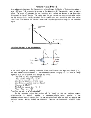
If the electronic circuit uses the Transistor as a Switch, then the biasing of the transistor, either it
is an NPN or a PNP is arranged to operate at the sides of the V-I characteristics curves as shown
below. The areas of operation for the transistor as a switch are known as the Saturation
Region and the Cut-off Region. This means then that we can use the operating Q-point biasing
and the voltage divider circuitry required for the amplification, as a transistor switch by moving
it back and forth between the fully-OFF that is the cut-off region and the fully-ON the saturation
region.
Transistor operates as an "open switch".
In the cutoff region the operating conditions of the transistor are zero input base current ( IB ),
the zero output collector current ( IC ) and maximum collector voltage ( VCE ). So there is a large
depletion layer and no current flows through the device.
· The input and Base are grounded (0v)
· Base-Emitter voltage VBE < 0.7V
· Base-Emitter junction is reverse biased
· Base-Collector junction is reverse biased
· Transistor is fully-OFF
· No Collector current flows ( IC = 0 )
· VOUT = VCE = VCC = "1".
Transistor operates as a "closed switch"
· In the saturation region the transistor will be biased so that the maximum amount
of base current is applied, resulting in maximum collector current resulting in the
minimum collector emitter voltage drop. So the depletion layer being as small as possible and
maximum current flowing through the transistor. Therefore the transistor is switched "Fully-
ON".
2. · The input and Base are connected to VCC
· Base-Emitter voltage VBE > 0.7V
· Base-Emitter junction is forward biased
· Base-Collector junction is forward biased
· Transistor is "fully-ON" (saturation region)
· Max Collector current flows (IC = Vcc/RL)
· VCE = 0 (ideal saturation)
· VOUT = VCE = "0"
Applications:
Transistor switches are widely used for controlling the high power devices such as
motors, solenoids or lamps. Transistor switches can also used in digital electronics and logic
gate circuits for there control.
Astable Multivibrator:
This is also called free running relaxation oscillator.
Used to generate square waveform.
Two identical NPN transistors Q1 and Q2 are used
RC1 = RC2 = RC ; R1 = R2 = R ; C1 = C2 = C ;
Transistor Q1 is biased through VCC via resistor RC1.
Transistor Q2 is biased through VCC via resistor RC2.
The output of Q1 is coupled to the input of transistor Q2 through capacitor C1.
The output of Q2 is coupled to the input of transistor Q1 through capacitor C2.
1800 phase shift is provided by the amplifier and the other 1800 phase shift is provided
by the capacitor. Hence the feedback signal has a total of 3600 phase shift. Thus the
feedback is positive and works as an oscillator.
Circuit operation:
When D.C. supply is switched ON, one of the transistor will start conducting more than
the other due to some imbalance in the circuit. If Q1 starts conducting, it is in Saturation
and transistor Q2 is in Cut-off.
When Q1 is ON and Q2 is OFF, the capacitor is charging towards the voltage VCC through
R1. The charging takes place exponentially with time constant R1.C1.
Since the base of Q1 is connected to capacitor C1, voltage at VB2 increases.
This leads to transistor Q2 to operate at saturation and its collector voltage VC1 falls and
hence cuts-off the transistor Q1.
Thus, the output of the transistor continuously switches between On and OFF states,
generating a square wave.
3. Applications:
Multivibrators Used in electronic circuits such as computers, control systems and
communication systems.
Astable Multivibrators are used as
1. Square wave generators
2. Voltage to frequency converters
3. Pulse Synchronisation
Bistable Multivibrator
This is also called flip-flop.
It has two stable states.
The two states are maintained as long as no external trigger is applied.
When an external trigger or a short pulse is applied to any one of the inputs, the Set or
Reset state is attained by the circuit.
Two identical NPN transistors Q1 and Q2 are used
RC1 = RC2 = RC ; R1 = R2 = R ; C1 = C2 = C ;
Transistor Q1 is biased through VCC via resistor RC1.
Transistor Q2 is biased through VCC via resistor RC2.
4. The output of Q1 is coupled to the input of transistor Q2 through Resistor R1
The output of Q2 is coupled to the input of transistor Q1 through Resistor R2
The capacitors C1 and C2 are speed up capacitors, which increases the speed of the
circuit in making abrupt transition from one stable state to another.
The base resistors R3 and R4 are connected to common source –VBB.
The output is available at the two collector terminals of the transistors, which are
complements of each other.
Circuit operation:
When D.C. supply is switched ON, one of the transistor will start conducting more than
the other due to some imbalance in the circuit.
If Q1 starts conducting, it is in Saturation (ON) and transistor Q2 is in Cut-off(OFF).
This is a stable state of the circuit, which will remain in this state till a trigger pulse is
applied.
A pulse applied at Reset input causes the transistor Q2 to conduct. As the collector
voltage of this transistor falls, Q1 goes to cut-off. Thus, Q2 ON and Q1 is OFF.
A pulse applied at Set input causes the transistor Q1 to conduct. As the collector voltage
of this transistor falls, Q2 goes to cut-off. Thus, Q1 ON and Q2 is OFF.
Thus, the collector output of the transistor changes its state when Set and Reset inputs
are given, and these states are stable as long as no trigger is applied, thus storing the
state.
Applications:
Used as Flip-flops in digital circuits.
Used as memory elements in Shift registers, counters etc.
Generation and processing of pulse type waveforms