The document discusses various types of nano devices and their operation. It describes resonant tunneling diode (RTD) which consists of a double barrier structure and exhibits peaks and valleys in current as electron energy passes quantum bound states. Resonant tunneling transistor (RTT) controls large current using small gate voltage. A single-electron transistor (SET) switches current using single electron charge on its gate. Other devices discussed include fin-shaped field-effect transistor (FinFET) and nanowire field-effect transistor (nanowire FET) which have better control of the channel using their 3D gate structure. Nano devices are used in various fields including medical, military and agriculture.
1. PREPARED BY : G
VANITHA
MTECH ECE
PONDICHERRY
UNIVERSITY
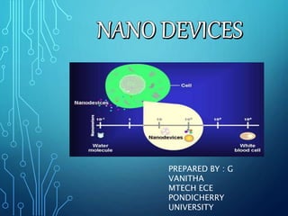
2. NANO DEVICES
• A Nano device is a device with at least one overall dimension in
the nanoscale, or comprising one or more nanoscale
components essential to its operation.
• It have ability to enhance energy conversion, control pollution,
produce food, and improve human health and longevity.
3. • Large collection of Nano devices connected to the internet eg.
nanobots and nanosensors
• Nano devices are used in different fields like medical, military,
agriculture etc.
• For communication all devices will be connected together through
internet
• Some of the nano devices are
oResonant tunneling diode
oResonant tunneling transistor
oSET
oFin FET
oNanowire FET
4. • It consists of double barrier structure with emitter and
collector contact.
• Energy band diagram of RTD with potential barriers or well in
the conduction or valance band - heterojunction
semiconductor system
5. • Resonant tunneling –two barriers –
located close to each other
• It is made up of single quantum
well structure surrounded by very
thin barriers called as double
barrier structure
• Electron –holes carriers a discrete
energy values inside the quantum
well.
• An RTD can be fabricated using
many different type of
materials(such as III-V, type VI, II-
VI semiconductor).
6. RTD operation
• Incident electrons have energy E and the quasi bound
states have energy En slightly above E
• E , tunneling when E=E1, I , positive resistance, peak
• E , I , negative resistance, valley
• Peaks and valleys occur whenever E approaches and
passes by the quasi bound states En.
7. RTD advantages
• Intrinsic disability and high speed switching capability
• Low power consumption
• Small device footprint
• increased functionality
8. • Resonant tunneling transistor
(RTT) as three-terminal
configuration in which a small
gate voltage can control a large
current across the device.
• RTT can perform as both switch
and amplifier
• RTD’s and RTT’s can have
multiple on and off states
associated with multiple discrete
quantum levels inside the
potential well on a very small or
very narrow island.
9. • Fig b shows Barriers in device create potential well around
the island, prevent charge from flowing through the device,
when it is under a voltage bias
• Fig C shows the gate electrode is charged, lowering the
energy for all the states in the well and bringing them into
resonance with the mobile electrons in the occupied
conduction band in the source, so that an electron current
can be transmitted through the device.
• The hybrid RTT also exhibits multistate behavior—the
drain current can be switched on and off several times for
various values of the bias voltage.
10. • A single-electron transistor (SET) is a three-terminal
device, with gate, source, and drain.
• An SET switches the source-to-drain current on and off in
response to small changes in the charge on the gate
amounting to a single electron or less
11. • In this channel is replaced by a small dot
• The dot is separated from source and drain by thin insulators
• Electron tunnels in to steps:
Source dot drain
• The gate voltage Vg is used to control the charge on the gate-
dot capacitor
• Increasing the gate voltage to a critical value suddenly allows
current to flow from source to drain, but further increase turns
off the current
• Additional increases in gate voltage repeat this on/off cycle
12. Advantages of SET
• High operating speed
• High sensitivity
• Low energy consumption
• Compact size with simplified circuit
Disadvantages of SET
• Can be operated in room temperature
• Co-tunneling
• Difficult to fabricate
13. • It stands for a fin-shaped field-effect transistor.
• Fin because it has a fin-shaped body – the silicon fin that
forms the transistor. Field-effect because an electric field
controls the conductivity of the material.
• It is a non-planar device.
• It is also called 3D for
having a third dimension.
14. • FinFETs are 3d structures that rise above the substrate and
resemble a fin.
• The 'fins' form the source and drain, enable more volume than
a traditional planar transistor for the same area.
• The gate wraps around the fin, gives more control of the
channel.
• So very little current to leak through the body when the
device is in the 'off' state. This also allows the use of lower
threshold voltages and it results in better performance and
lower power dissipation.
• Gate structure provides improved electrical control over the
channel conduction and it helps reduce leakage current levels
and overcomes some other short-channel effects..
15. Advantages of FinFET
• Lower static leakage current and Higher drain current
• Faster switching speed
• Lower switching voltage
• Low power consumption
Disadvantages of FinFET
• Higher parasitics due to 3-D profile
• Very high capacitances
• High fabrication cost
Application of FinFET
It include home computers, laptops, tablets, smartphones,
wearables, high-end networks, automotive, and more.
16. • Nanowire is a wire-like structure with diameter or lateral
dimension of nanometer(10-9m)
• Various material systems can be used to fabricate
nanowires e.g. Silver, Gold, Copper, …, etc. (metal)
Si, Ge, GaAs, GaN, …, etc. (semiconductor)
17. • Nanowire FET : field effect transistor(FET) using nanowire
• The current from the source to the drain is turned on and off
by the voltage applied to the gate.
• Because the gate in nanowires is surrounding the channel, it
can control the electrostatics of the channel more efficiently
than the conventional MOSFET.
• Electron density in the channel increases as diameter of
nanowire increases.
• → Drain current increases at large diameter nanowire.
18. Application Of Nanowire FET
• Silicon nanowires configured field-effect transistors were
used as a biosensor.
• To investigate protein–protein interaction and DNA
hybridization.
• For viral infection monitoring, early cancer detection, and
biomarker detection.
• To monitor electrical and transmitter signals from living cells.
• Synthesize a 3D-localized bioprobe to record intracellular
potentials.