POROSITY IN DEPOSITED MATERIAL - ADDITIVE MANUFACTURING
•
1 gefällt mir•40 views

An interest document of LPW TECHNOLOGY about a case study of porosity in deposited material of a product made with additive manufacturing.

Empfohlen
Weitere ähnliche Inhalte
Was ist angesagt?
Was ist angesagt? (18)
Ähnlich wie POROSITY IN DEPOSITED MATERIAL - ADDITIVE MANUFACTURING
Ähnlich wie POROSITY IN DEPOSITED MATERIAL - ADDITIVE MANUFACTURING (20)
Kürzlich hochgeladen
Kürzlich hochgeladen (20)
POROSITY IN DEPOSITED MATERIAL - ADDITIVE MANUFACTURING
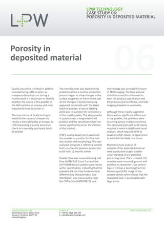
- 1. 06Quality assurance is critical in additive manufacturing (AM) so when an unexpected result occurs during a routine build it is important to identify whether the source is the powder or the AM machine or process and most importantly how to correct it. The importance of timely testing to establish the cause of unexpected results is exemplified by an enquiry to LPW requesting a quality assurance check on a recently purchased batch of powder. The manufacturer was experiencing problems where a routine production process began to show changes in the surface roughness of the finished part. As the changes in build processing appeared to coincide with the latest batch of powder, a natural starting point was to question the consistency of the metal powder. The alloy powder in question was a long established product and the specification had not varied significantly across the lifetime of the product. LPW’s quality department examined the powder in question for flow, size distribution and morphology. This was analysed alongside a reference sample from a successful previous production build from 12 months earlier. Powder flow was measured using Hall Flow (ASTM B213) and Carney Flow (ASTM B964) each powder gave results within specification, indicating that the powders did not have fundamentally different flow characteristics. Size distribution was measured by Laser Size Diffraction (ASTM B822), and morphology was assessed by means of SEM imaging. The flow and size distribution results conformed to both the product specification and the previous test certificate, and SEM imaging revealed no anomalies. Although these results suggested there was no significant differences in the powder, the problems were occurring across multiple machines. The observed poor part build clearly required a more in depth root cause analysis, which required LPW to develop a DoE, design of experiment to establish the likely root cause. Microstructural analysis of samples of the deposited material were conducted to gain a better understanding of any potential processing issue. Once received, the samples were mounted, ground and polished to reveal the cross section. Figure 1 shows a Scanning Electron Microscope (SEM) image of the sample section which shows that the deposited layer is punctuated with large pores. LPW TECHNOLOGY CASE STUDY 06: POROSITY IN DEPOSITED MATERIAL Porosity in deposited material LPW TECHNOLOGY LTD 16 Berkeley Court, Manor Park Runcorn, Cheshire WA7 1TQ United Kingdom LPW TECHNOLOGY LTDCONTACT T: +44 (0) 1928 240 530 E: sales@lpwtechnology.com
- 2. One understandable explanation is that the powder being included in the deposited layer is porous. The powder particles are between 20-53 microns in diameter and measurements of the pores reveal them to be 30-50 microns across, so are highly unlikely to be contained stably within a powder particle. Since powder porosity would also not explain poor surface finish, the machine processing conditions were carefully investigated. A large retained sample of a previous batch of powder which was known to process satisfactorily was used in order to ensure a like for like comparison. After replacing a key component of the deposition system across all machines, that build quality was restored to output products that passed the stringent quality controls. It was confirmed that component deterioration across the machines was the root cause. Outcome Initial flow measurements had indicated that the root cause of poor build was unlikely to be the powder, but it was only by applying in-house industry expertise in AM processing and thorough analysis capabilities of both powder and part, that LPW was able to deliver confidence and a holistic processing solution. LPW TECHNOLOGY CASE STUDY 06: POROSITY IN DEPOSITED MATERIAL LPW TECHNOLOGY LTD 16 Berkeley Court, Manor Park Runcorn, Cheshire WA7 1TQ United Kingdom LPW TECHNOLOGY LTDCONTACT T: +44 (0) 1928 240 530 E: sales@lpwtechnology.com Figure 1 – SEM micrograph of deposited layer-substrate interface