SlideShare ist ein Scribd-Unternehmen logo
1 von 4
Downloaden Sie, um offline zu lesen
I. Processes to work with Pel


                        Design of
                        Drawing

                      Silk-screening
                            y/o..

                       Cut of Vinyl


                      Unite image with support


                       Cut sheet of Pel


                       Laminate Pel


                       Cabling


                       Finalization
                      / Installation
II. General Diagram


Red
220V                  Power
                      generator
                                  Pel
III. Production of Pel

A1. Printing for silk-screening
1) Print along the film (printing for coat)
2) Order the colors of the printing according to the design
3) Use the translucent printing where you want to have colored light
4) Use opaque or metallic ink except for where the Pel is going to be (This is to block light penetration)
5) It has to be printed mirror-inverted (to avoid scratching of the printing)
* Advantages of the silk-screen printing: - Low price in high quantity.
                            - Excellent appearance and ending
                            - High quality
 * Disadvantages: Expensive in low quantities
                                                                       Transparent


B2. Using vinyl cut                                                                           Light Block
1) Design the graphic in “coat” mode using appropriate programs (Illustrator, CorelDraw, etc)
* Note: Select the appropriate program to plotter the cut
2It might be necessary to place 2 vinyl cuts on top of each other to block unnecessary light.
 3) Cut computerized, montage the vinyl over the Pel.
3. Attach the design to the support (film, met acryl)
1) You can moisten the support before you place the vinyl
2) Stick on all the vinyl cuts in the correct order (translucent and opaque)
3) Dry and avoid any left over humidity that enters in the contact with the Pel with being laminated


4. Cut the Pel sheet
1) Cut the Pel according to the design, always leaving some edges with the metalized contacts
2) Attach around the copper to the poles conductive of Pel
3) If the Pel is laminated, allow to expose areas of the conductive poles, using an utter carefully
•Note: You have to be careful not to cut the poles of the copper. The covers of the Pel sheet are very fragile
5) Attach the Pel to the meta acryl, film, etc that carry the design mask
6) Join the cables together with the tins over the coppered poles
(Excessive time with the soldering burns the Pel) y cable the connections
                                                                                    Connection poles in the
                                                                                    back of the Pel, using
5. Cabling                                                                          copper tape
1) To switch on permanently all areas of the Pel, and connect parallel (diagram A)
2) Sequence: With a cable plan of 5 conductors, use a common pole to connect the resistants to every unit per
canal. Diagram B
3) The Pel does not have polarity. Humidity ruins the Pel. The over current cuts the utility life (100VAC 400Hz)


                                    Diagram A                                            Diagram B

Weitere ähnliche Inhalte

Ähnlich wie Pel process application

Double sided PCB manufacturing
Double sided PCB manufacturingDouble sided PCB manufacturing
Double sided PCB manufacturingAditya Todi
 
Acadia2011 - Red Rabbit
Acadia2011 - Red RabbitAcadia2011 - Red Rabbit
Acadia2011 - Red Rabbitjoshuazabel
 
Building2.4 g hz10elementyagiantenna
Building2.4 g hz10elementyagiantennaBuilding2.4 g hz10elementyagiantenna
Building2.4 g hz10elementyagiantennaProvis Chonburi
 
Working casts and dies
Working casts and diesWorking casts and dies
Working casts and diesLama K Banna
 
Casting unit 1 notes
Casting unit 1 notesCasting unit 1 notes
Casting unit 1 notesrmkcet
 
Impression Techniques in Fixed partial denture
Impression Techniques in Fixed partial dentureImpression Techniques in Fixed partial denture
Impression Techniques in Fixed partial dentureDr.Richa Sahai
 
Ms for-finish-painting-work
Ms for-finish-painting-workMs for-finish-painting-work
Ms for-finish-painting-workthanhuce
 
Die materials and die systems
Die materials and die systemsDie materials and die systems
Die materials and die systemssmidsprostho
 
Polymer investment molding modified
Polymer investment molding modifiedPolymer investment molding modified
Polymer investment molding modifiedarun kumar
 
Experiences Olaya- Frasers-ID Package- Public Spaces
Experiences Olaya- Frasers-ID Package- Public SpacesExperiences Olaya- Frasers-ID Package- Public Spaces
Experiences Olaya- Frasers-ID Package- Public SpacesAmer El Malki
 
Chapter 1-IC Fabrication.pptx
Chapter 1-IC Fabrication.pptxChapter 1-IC Fabrication.pptx
Chapter 1-IC Fabrication.pptxKarthik Prof.
 
Multi Layer Printed Circuit Board Introduction and Manufacturing process
Multi Layer Printed Circuit  Board Introduction and Manufacturing processMulti Layer Printed Circuit  Board Introduction and Manufacturing process
Multi Layer Printed Circuit Board Introduction and Manufacturing processAditya Deshpande
 
IRJET- Cost Effective Manufacturing and Optimization of the Formula Student N...
IRJET- Cost Effective Manufacturing and Optimization of the Formula Student N...IRJET- Cost Effective Manufacturing and Optimization of the Formula Student N...
IRJET- Cost Effective Manufacturing and Optimization of the Formula Student N...IRJET Journal
 
Flipchip bonding.
Flipchip bonding.Flipchip bonding.
Flipchip bonding.venkata016
 
EE driving the cost out of your design
EE driving the cost out of your designEE driving the cost out of your design
EE driving the cost out of your designbmacforever
 

Ähnlich wie Pel process application (20)

Double sided PCB manufacturing
Double sided PCB manufacturingDouble sided PCB manufacturing
Double sided PCB manufacturing
 
Wax modeling
Wax modelingWax modeling
Wax modeling
 
Acadia2011 - Red Rabbit
Acadia2011 - Red RabbitAcadia2011 - Red Rabbit
Acadia2011 - Red Rabbit
 
3 foundry
3 foundry3 foundry
3 foundry
 
Building2.4 g hz10elementyagiantenna
Building2.4 g hz10elementyagiantennaBuilding2.4 g hz10elementyagiantenna
Building2.4 g hz10elementyagiantenna
 
Working casts and dies
Working casts and diesWorking casts and dies
Working casts and dies
 
Casting unit 1 notes
Casting unit 1 notesCasting unit 1 notes
Casting unit 1 notes
 
99997340.pdf
99997340.pdf99997340.pdf
99997340.pdf
 
Impression Techniques in Fixed partial denture
Impression Techniques in Fixed partial dentureImpression Techniques in Fixed partial denture
Impression Techniques in Fixed partial denture
 
Ms for-finish-painting-work
Ms for-finish-painting-workMs for-finish-painting-work
Ms for-finish-painting-work
 
Die materials and die systems
Die materials and die systemsDie materials and die systems
Die materials and die systems
 
Polymer investment molding modified
Polymer investment molding modifiedPolymer investment molding modified
Polymer investment molding modified
 
Experiences Olaya- Frasers-ID Package- Public Spaces
Experiences Olaya- Frasers-ID Package- Public SpacesExperiences Olaya- Frasers-ID Package- Public Spaces
Experiences Olaya- Frasers-ID Package- Public Spaces
 
Chapter 1-IC Fabrication.pptx
Chapter 1-IC Fabrication.pptxChapter 1-IC Fabrication.pptx
Chapter 1-IC Fabrication.pptx
 
Multi Layer Printed Circuit Board Introduction and Manufacturing process
Multi Layer Printed Circuit  Board Introduction and Manufacturing processMulti Layer Printed Circuit  Board Introduction and Manufacturing process
Multi Layer Printed Circuit Board Introduction and Manufacturing process
 
IRJET- Cost Effective Manufacturing and Optimization of the Formula Student N...
IRJET- Cost Effective Manufacturing and Optimization of the Formula Student N...IRJET- Cost Effective Manufacturing and Optimization of the Formula Student N...
IRJET- Cost Effective Manufacturing and Optimization of the Formula Student N...
 
Film strip ok
Film strip okFilm strip ok
Film strip ok
 
Flipchip bonding.
Flipchip bonding.Flipchip bonding.
Flipchip bonding.
 
EE driving the cost out of your design
EE driving the cost out of your designEE driving the cost out of your design
EE driving the cost out of your design
 
Design and Manufacturing Homework Help
Design and Manufacturing Homework HelpDesign and Manufacturing Homework Help
Design and Manufacturing Homework Help
 

Mehr von LTi worldwide

LTi robotics logicas-es
LTi robotics logicas-esLTi robotics logicas-es
LTi robotics logicas-esLTi worldwide
 
LTi llamador 911 bench
LTi llamador 911 benchLTi llamador 911 bench
LTi llamador 911 benchLTi worldwide
 
LTi folder español spanish
LTi folder español spanishLTi folder español spanish
LTi folder español spanishLTi worldwide
 
LTi luminescent materials
LTi luminescent materialsLTi luminescent materials
LTi luminescent materialsLTi worldwide
 
Pel Panels Electro-Luminous
Pel Panels Electro-LuminousPel Panels Electro-Luminous
Pel Panels Electro-LuminousLTi worldwide
 
LTi interactive products
LTi interactive productsLTi interactive products
LTi interactive productsLTi worldwide
 
Lbar Interactive bar tables
Lbar Interactive bar tablesLbar Interactive bar tables
Lbar Interactive bar tablesLTi worldwide
 

Mehr von LTi worldwide (11)

LT-ifloor
LT-ifloorLT-ifloor
LT-ifloor
 
LTi robotics logicas-es
LTi robotics logicas-esLTi robotics logicas-es
LTi robotics logicas-es
 
LTi llamador 911 bench
LTi llamador 911 benchLTi llamador 911 bench
LTi llamador 911 bench
 
LTi ledsigns
LTi ledsignsLTi ledsigns
LTi ledsigns
 
LTi folder español spanish
LTi folder español spanishLTi folder español spanish
LTi folder español spanish
 
Matching wrj om r
Matching wrj om rMatching wrj om r
Matching wrj om r
 
Bloq cell en
Bloq cell enBloq cell en
Bloq cell en
 
LTi luminescent materials
LTi luminescent materialsLTi luminescent materials
LTi luminescent materials
 
Pel Panels Electro-Luminous
Pel Panels Electro-LuminousPel Panels Electro-Luminous
Pel Panels Electro-Luminous
 
LTi interactive products
LTi interactive productsLTi interactive products
LTi interactive products
 
Lbar Interactive bar tables
Lbar Interactive bar tablesLbar Interactive bar tables
Lbar Interactive bar tables
 

Pel process application

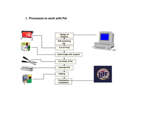
  • 1. I. Processes to work with Pel Design of Drawing Silk-screening y/o.. Cut of Vinyl Unite image with support Cut sheet of Pel Laminate Pel Cabling Finalization / Installation
  • 2. II. General Diagram Red 220V Power generator Pel
  • 3. III. Production of Pel A1. Printing for silk-screening 1) Print along the film (printing for coat) 2) Order the colors of the printing according to the design 3) Use the translucent printing where you want to have colored light 4) Use opaque or metallic ink except for where the Pel is going to be (This is to block light penetration) 5) It has to be printed mirror-inverted (to avoid scratching of the printing) * Advantages of the silk-screen printing: - Low price in high quantity. - Excellent appearance and ending - High quality * Disadvantages: Expensive in low quantities Transparent B2. Using vinyl cut Light Block 1) Design the graphic in “coat” mode using appropriate programs (Illustrator, CorelDraw, etc) * Note: Select the appropriate program to plotter the cut 2It might be necessary to place 2 vinyl cuts on top of each other to block unnecessary light. 3) Cut computerized, montage the vinyl over the Pel.
  • 4. 3. Attach the design to the support (film, met acryl) 1) You can moisten the support before you place the vinyl 2) Stick on all the vinyl cuts in the correct order (translucent and opaque) 3) Dry and avoid any left over humidity that enters in the contact with the Pel with being laminated 4. Cut the Pel sheet 1) Cut the Pel according to the design, always leaving some edges with the metalized contacts 2) Attach around the copper to the poles conductive of Pel 3) If the Pel is laminated, allow to expose areas of the conductive poles, using an utter carefully •Note: You have to be careful not to cut the poles of the copper. The covers of the Pel sheet are very fragile 5) Attach the Pel to the meta acryl, film, etc that carry the design mask 6) Join the cables together with the tins over the coppered poles (Excessive time with the soldering burns the Pel) y cable the connections Connection poles in the back of the Pel, using 5. Cabling copper tape 1) To switch on permanently all areas of the Pel, and connect parallel (diagram A) 2) Sequence: With a cable plan of 5 conductors, use a common pole to connect the resistants to every unit per canal. Diagram B 3) The Pel does not have polarity. Humidity ruins the Pel. The over current cuts the utility life (100VAC 400Hz) Diagram A Diagram B