SlideShare ist ein Scribd-Unternehmen logo
1 von 13
SUBMITTED BY
FAIZAN AHMAD , ZIA UR REHMAN ,USAMA ANWAR
SUBMITTED TO
DR. WASEEM
• Diode formation
• No biased
• Forward biased
• Reverse biased
• Characteristic curve
• Reverse breakdown
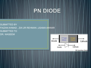
• A PN diode is formed by joining P-type material and N-
type material together.
• There are three possibilities:
• No Biased
• Forward Biased
• Reverse Biased
• What is biased?
• Application of external voltage across two terminal.
• Symbol of diode is
• Process of moving of majority
charge carrier from Higher to
Lower concentration is known as
diffusion and the current is
called Diffusion current.
• Depletion region is formed after recombination
process, in which immobile ions are surface out.
Holes
• No further movement of charges.
• +ve immobile ions repel hole from P-side,
• -ve immobile ions will repel electron from N- side.
• Hence the depletion region act as barrier.
• There is drift current due to minority charge carrier and in
the direction of electric field.
Depletion RegionP N
e
• +ve terminal of battery will repels the holes and –ve
terminal repels the electrons towards the depletion
region, because of this depletion region decrease.
• The flood of electron will pass through the junction and
current rises exponentially.
New Depletion Region
Id
Id
Depletion region
• +ve terminal of battery will attract the electrons and the –
ve terminal will attract the holes, due to this the depletion
region increase.
• There is only one current due to minority charge carrier,
known as reverse saturation current.
New region
Is Is
- +
• Diode current relation is given as:
ID=IS(eVD/nVT -1)
IS=Reverse saturation current.
VD= Biased Voltage.
n= Ideality Factor.
VT=KTK/q
TK= Temperature in Kelvin.
K=1.38*10-23J/K
• For No Biased VD=0
• ID=IS(e0- 1)
• ID=IS(1- 1)
• ID=0
• In no biased there is no current through the diode as
shown in diagram.
Ge Si
G eSi
0.3 0.7
• For Forward Biased VD increase & Potential Barrier
decrease.
• For Silicon Potential Barrier 0.7 and for Germanium 0.3.
• When VD< Potential Barrier,
• no current flow.
• When VD>= Potential Barrier current will exponentially
rise as shown in fig.
0.3 0.7
siGe
• For reversed Biased
• VD<0 so,
ID=IS(eVD/nVT -1)
Become –ve and so
small we can neglect.
• ID=IS(0 -1)
• ID=-IS
• In reverse Biased condition we know that there is only reverse
saturation current due to minority charge carrier as shown in
fig.
S
i
Ge
GeSi
0.3 0.7
• When we increase the reverse Biased voltage at higher
value, There is sudden rise in current as show in above
fig.
• This is known as breakdown voltage. At this breakdown
of diode occur.
• What is breakdown?
• When we increase the voltage, electron will acquire very
high Kinetic energy. They will break the covalent bond
and become free. This free electron collide with other
electron and free then the process continue like the
chain.
• Peak inverse voltage:
• Maximum reverse biased voltage that can be applied
across the diode before entering to the break down
region.
Pn diode presentation

Weitere ähnliche Inhalte

Was ist angesagt?

Was ist angesagt? (20)

Tunnel diode
Tunnel diodeTunnel diode
Tunnel diode
 
Pn junction
Pn junctionPn junction
Pn junction
 
Tunnel Diode (Esaki Diode )
Tunnel Diode (Esaki Diode )Tunnel Diode (Esaki Diode )
Tunnel Diode (Esaki Diode )
 
P n junction characteristics
P n junction characteristicsP n junction characteristics
P n junction characteristics
 
Pn junction diodes (presentation)
Pn junction diodes (presentation)Pn junction diodes (presentation)
Pn junction diodes (presentation)
 
Diode
DiodeDiode
Diode
 
Zener diode
Zener diodeZener diode
Zener diode
 
Zener diode as a voltage Regulator
Zener diode as a voltage RegulatorZener diode as a voltage Regulator
Zener diode as a voltage Regulator
 
PN junction
PN  junctionPN  junction
PN junction
 
EC6202 ELECTRONIC DEVICES AND CIRCUITS Unit 2
EC6202 ELECTRONIC DEVICES AND CIRCUITS Unit 2EC6202 ELECTRONIC DEVICES AND CIRCUITS Unit 2
EC6202 ELECTRONIC DEVICES AND CIRCUITS Unit 2
 
pn junction diodes
pn junction diodespn junction diodes
pn junction diodes
 
Diodes
Diodes Diodes
Diodes
 
Application of diode
Application of diodeApplication of diode
Application of diode
 
Presentation on JFET
Presentation on JFETPresentation on JFET
Presentation on JFET
 
The p n Junction Diode (Basic Electronics)
The p n Junction Diode (Basic Electronics) The p n Junction Diode (Basic Electronics)
The p n Junction Diode (Basic Electronics)
 
Rec101 unit 1 (part ii) pn junction diode
Rec101 unit 1 (part ii)  pn junction diodeRec101 unit 1 (part ii)  pn junction diode
Rec101 unit 1 (part ii) pn junction diode
 
Zener diode as voltage regulator
Zener diode as voltage regulatorZener diode as voltage regulator
Zener diode as voltage regulator
 
Topic 3 pn_junction_and_diode
Topic 3 pn_junction_and_diodeTopic 3 pn_junction_and_diode
Topic 3 pn_junction_and_diode
 
P n junction--eema
P n junction--eemaP n junction--eema
P n junction--eema
 
shortkey diode
shortkey diodeshortkey diode
shortkey diode
 

Ähnlich wie Pn diode presentation

Ähnlich wie Pn diode presentation (20)

UNIT II.ppt
UNIT II.pptUNIT II.ppt
UNIT II.ppt
 
Electronics ichapter1
Electronics ichapter1Electronics ichapter1
Electronics ichapter1
 
Basic electronics and electrical first year engineering
Basic electronics and electrical first year engineeringBasic electronics and electrical first year engineering
Basic electronics and electrical first year engineering
 
EC 8353 EDC
EC 8353 EDCEC 8353 EDC
EC 8353 EDC
 
Electronic devices circuits
Electronic devices circuitsElectronic devices circuits
Electronic devices circuits
 
Chapter 5: Diode
Chapter 5: DiodeChapter 5: Diode
Chapter 5: Diode
 
EST 130, PN Junction Diodes
EST 130, PN Junction DiodesEST 130, PN Junction Diodes
EST 130, PN Junction Diodes
 
Basic electronics (p-n Junction)
Basic electronics (p-n Junction)Basic electronics (p-n Junction)
Basic electronics (p-n Junction)
 
Lecture 5
Lecture 5Lecture 5
Lecture 5
 
Bsc 1 cbcs e1 unit 2
Bsc 1 cbcs e1 unit 2Bsc 1 cbcs e1 unit 2
Bsc 1 cbcs e1 unit 2
 
UNIT4.pptx
UNIT4.pptxUNIT4.pptx
UNIT4.pptx
 
Chapter2
Chapter2Chapter2
Chapter2
 
Pn junction diode by sarmad baloch
Pn junction diode by sarmad balochPn junction diode by sarmad baloch
Pn junction diode by sarmad baloch
 
BASIC ELECTRONICS!!
BASIC ELECTRONICS!!BASIC ELECTRONICS!!
BASIC ELECTRONICS!!
 
Electronic Devices - Special Diodes - Unit 1.pptx
Electronic Devices - Special Diodes - Unit 1.pptxElectronic Devices - Special Diodes - Unit 1.pptx
Electronic Devices - Special Diodes - Unit 1.pptx
 
task_2.pptx
task_2.pptxtask_2.pptx
task_2.pptx
 
unit-2.pdf
unit-2.pdfunit-2.pdf
unit-2.pdf
 
Pn junction diode
Pn junction diodePn junction diode
Pn junction diode
 
10546931.ppt
10546931.ppt10546931.ppt
10546931.ppt
 
PN Diode VI Characteristics.pptx
PN Diode VI Characteristics.pptxPN Diode VI Characteristics.pptx
PN Diode VI Characteristics.pptx
 

Mehr von Bilawal Fiaz

LED-light emitting diode
LED-light emitting diodeLED-light emitting diode
LED-light emitting diodeBilawal Fiaz
 
Tunnel Diode presentation
Tunnel Diode presentationTunnel Diode presentation
Tunnel Diode presentationBilawal Fiaz
 
Photo diode presentation
Photo diode presentationPhoto diode presentation
Photo diode presentationBilawal Fiaz
 
Laser diode presentation
Laser diode presentationLaser diode presentation
Laser diode presentationBilawal Fiaz
 
zener diode presentation
zener diode presentationzener diode presentation
zener diode presentationBilawal Fiaz
 
Light emitting diode presentation
Light emitting diode presentationLight emitting diode presentation
Light emitting diode presentationBilawal Fiaz
 
LED-light emitting diode
LED-light emitting diodeLED-light emitting diode
LED-light emitting diodeBilawal Fiaz
 
Registers-shift register
Registers-shift registerRegisters-shift register
Registers-shift registerBilawal Fiaz
 

Mehr von Bilawal Fiaz (10)

Computer Buses
Computer BusesComputer Buses
Computer Buses
 
LED-light emitting diode
LED-light emitting diodeLED-light emitting diode
LED-light emitting diode
 
Tunnel Diode presentation
Tunnel Diode presentationTunnel Diode presentation
Tunnel Diode presentation
 
Photo diode presentation
Photo diode presentationPhoto diode presentation
Photo diode presentation
 
Zener diode pptx
Zener diode pptxZener diode pptx
Zener diode pptx
 
Laser diode presentation
Laser diode presentationLaser diode presentation
Laser diode presentation
 
zener diode presentation
zener diode presentationzener diode presentation
zener diode presentation
 
Light emitting diode presentation
Light emitting diode presentationLight emitting diode presentation
Light emitting diode presentation
 
LED-light emitting diode
LED-light emitting diodeLED-light emitting diode
LED-light emitting diode
 
Registers-shift register
Registers-shift registerRegisters-shift register
Registers-shift register
 

Kürzlich hochgeladen

Online electricity billing project report..pdf
Online electricity billing project report..pdfOnline electricity billing project report..pdf
Online electricity billing project report..pdfKamal Acharya
 
"Lesotho Leaps Forward: A Chronicle of Transformative Developments"
"Lesotho Leaps Forward: A Chronicle of Transformative Developments""Lesotho Leaps Forward: A Chronicle of Transformative Developments"
"Lesotho Leaps Forward: A Chronicle of Transformative Developments"mphochane1998
 
Thermal Engineering Unit - I & II . ppt
Thermal Engineering  Unit - I & II . pptThermal Engineering  Unit - I & II . ppt
Thermal Engineering Unit - I & II . pptDineshKumar4165
 
DeepFakes presentation : brief idea of DeepFakes
DeepFakes presentation : brief idea of DeepFakesDeepFakes presentation : brief idea of DeepFakes
DeepFakes presentation : brief idea of DeepFakesMayuraD1
 
A Study of Urban Area Plan for Pabna Municipality
A Study of Urban Area Plan for Pabna MunicipalityA Study of Urban Area Plan for Pabna Municipality
A Study of Urban Area Plan for Pabna MunicipalityMorshed Ahmed Rahath
 
AIRCANVAS[1].pdf mini project for btech students
AIRCANVAS[1].pdf mini project for btech studentsAIRCANVAS[1].pdf mini project for btech students
AIRCANVAS[1].pdf mini project for btech studentsvanyagupta248
 
GEAR TRAIN- BASIC CONCEPTS AND WORKING PRINCIPLE
GEAR TRAIN- BASIC CONCEPTS AND WORKING PRINCIPLEGEAR TRAIN- BASIC CONCEPTS AND WORKING PRINCIPLE
GEAR TRAIN- BASIC CONCEPTS AND WORKING PRINCIPLEselvakumar948
 
DC MACHINE-Motoring and generation, Armature circuit equation
DC MACHINE-Motoring and generation, Armature circuit equationDC MACHINE-Motoring and generation, Armature circuit equation
DC MACHINE-Motoring and generation, Armature circuit equationBhangaleSonal
 
Bhubaneswar🌹Call Girls Bhubaneswar ❤Komal 9777949614 💟 Full Trusted CALL GIRL...
Bhubaneswar🌹Call Girls Bhubaneswar ❤Komal 9777949614 💟 Full Trusted CALL GIRL...Bhubaneswar🌹Call Girls Bhubaneswar ❤Komal 9777949614 💟 Full Trusted CALL GIRL...
Bhubaneswar🌹Call Girls Bhubaneswar ❤Komal 9777949614 💟 Full Trusted CALL GIRL...Call Girls Mumbai
 
data_management_and _data_science_cheat_sheet.pdf
data_management_and _data_science_cheat_sheet.pdfdata_management_and _data_science_cheat_sheet.pdf
data_management_and _data_science_cheat_sheet.pdfJiananWang21
 
1_Introduction + EAM Vocabulary + how to navigate in EAM.pdf
1_Introduction + EAM Vocabulary + how to navigate in EAM.pdf1_Introduction + EAM Vocabulary + how to navigate in EAM.pdf
1_Introduction + EAM Vocabulary + how to navigate in EAM.pdfAldoGarca30
 
HAND TOOLS USED AT ELECTRONICS WORK PRESENTED BY KOUSTAV SARKAR
HAND TOOLS USED AT ELECTRONICS WORK PRESENTED BY KOUSTAV SARKARHAND TOOLS USED AT ELECTRONICS WORK PRESENTED BY KOUSTAV SARKAR
HAND TOOLS USED AT ELECTRONICS WORK PRESENTED BY KOUSTAV SARKARKOUSTAV SARKAR
 
Thermal Engineering-R & A / C - unit - V
Thermal Engineering-R & A / C - unit - VThermal Engineering-R & A / C - unit - V
Thermal Engineering-R & A / C - unit - VDineshKumar4165
 
Introduction to Serverless with AWS Lambda
Introduction to Serverless with AWS LambdaIntroduction to Serverless with AWS Lambda
Introduction to Serverless with AWS LambdaOmar Fathy
 
Kuwait City MTP kit ((+919101817206)) Buy Abortion Pills Kuwait
Kuwait City MTP kit ((+919101817206)) Buy Abortion Pills KuwaitKuwait City MTP kit ((+919101817206)) Buy Abortion Pills Kuwait
Kuwait City MTP kit ((+919101817206)) Buy Abortion Pills Kuwaitjaanualu31
 
Employee leave management system project.
Employee leave management system project.Employee leave management system project.
Employee leave management system project.Kamal Acharya
 
Hospital management system project report.pdf
Hospital management system project report.pdfHospital management system project report.pdf
Hospital management system project report.pdfKamal Acharya
 
Unit 4_Part 1 CSE2001 Exception Handling and Function Template and Class Temp...
Unit 4_Part 1 CSE2001 Exception Handling and Function Template and Class Temp...Unit 4_Part 1 CSE2001 Exception Handling and Function Template and Class Temp...
Unit 4_Part 1 CSE2001 Exception Handling and Function Template and Class Temp...drmkjayanthikannan
 
Computer Lecture 01.pptxIntroduction to Computers
Computer Lecture 01.pptxIntroduction to ComputersComputer Lecture 01.pptxIntroduction to Computers
Computer Lecture 01.pptxIntroduction to ComputersMairaAshraf6
 

Kürzlich hochgeladen (20)

Online electricity billing project report..pdf
Online electricity billing project report..pdfOnline electricity billing project report..pdf
Online electricity billing project report..pdf
 
"Lesotho Leaps Forward: A Chronicle of Transformative Developments"
"Lesotho Leaps Forward: A Chronicle of Transformative Developments""Lesotho Leaps Forward: A Chronicle of Transformative Developments"
"Lesotho Leaps Forward: A Chronicle of Transformative Developments"
 
Thermal Engineering Unit - I & II . ppt
Thermal Engineering  Unit - I & II . pptThermal Engineering  Unit - I & II . ppt
Thermal Engineering Unit - I & II . ppt
 
DeepFakes presentation : brief idea of DeepFakes
DeepFakes presentation : brief idea of DeepFakesDeepFakes presentation : brief idea of DeepFakes
DeepFakes presentation : brief idea of DeepFakes
 
A Study of Urban Area Plan for Pabna Municipality
A Study of Urban Area Plan for Pabna MunicipalityA Study of Urban Area Plan for Pabna Municipality
A Study of Urban Area Plan for Pabna Municipality
 
AIRCANVAS[1].pdf mini project for btech students
AIRCANVAS[1].pdf mini project for btech studentsAIRCANVAS[1].pdf mini project for btech students
AIRCANVAS[1].pdf mini project for btech students
 
GEAR TRAIN- BASIC CONCEPTS AND WORKING PRINCIPLE
GEAR TRAIN- BASIC CONCEPTS AND WORKING PRINCIPLEGEAR TRAIN- BASIC CONCEPTS AND WORKING PRINCIPLE
GEAR TRAIN- BASIC CONCEPTS AND WORKING PRINCIPLE
 
Cara Menggugurkan Sperma Yang Masuk Rahim Biyar Tidak Hamil
Cara Menggugurkan Sperma Yang Masuk Rahim Biyar Tidak HamilCara Menggugurkan Sperma Yang Masuk Rahim Biyar Tidak Hamil
Cara Menggugurkan Sperma Yang Masuk Rahim Biyar Tidak Hamil
 
DC MACHINE-Motoring and generation, Armature circuit equation
DC MACHINE-Motoring and generation, Armature circuit equationDC MACHINE-Motoring and generation, Armature circuit equation
DC MACHINE-Motoring and generation, Armature circuit equation
 
Bhubaneswar🌹Call Girls Bhubaneswar ❤Komal 9777949614 💟 Full Trusted CALL GIRL...
Bhubaneswar🌹Call Girls Bhubaneswar ❤Komal 9777949614 💟 Full Trusted CALL GIRL...Bhubaneswar🌹Call Girls Bhubaneswar ❤Komal 9777949614 💟 Full Trusted CALL GIRL...
Bhubaneswar🌹Call Girls Bhubaneswar ❤Komal 9777949614 💟 Full Trusted CALL GIRL...
 
data_management_and _data_science_cheat_sheet.pdf
data_management_and _data_science_cheat_sheet.pdfdata_management_and _data_science_cheat_sheet.pdf
data_management_and _data_science_cheat_sheet.pdf
 
1_Introduction + EAM Vocabulary + how to navigate in EAM.pdf
1_Introduction + EAM Vocabulary + how to navigate in EAM.pdf1_Introduction + EAM Vocabulary + how to navigate in EAM.pdf
1_Introduction + EAM Vocabulary + how to navigate in EAM.pdf
 
HAND TOOLS USED AT ELECTRONICS WORK PRESENTED BY KOUSTAV SARKAR
HAND TOOLS USED AT ELECTRONICS WORK PRESENTED BY KOUSTAV SARKARHAND TOOLS USED AT ELECTRONICS WORK PRESENTED BY KOUSTAV SARKAR
HAND TOOLS USED AT ELECTRONICS WORK PRESENTED BY KOUSTAV SARKAR
 
Thermal Engineering-R & A / C - unit - V
Thermal Engineering-R & A / C - unit - VThermal Engineering-R & A / C - unit - V
Thermal Engineering-R & A / C - unit - V
 
Introduction to Serverless with AWS Lambda
Introduction to Serverless with AWS LambdaIntroduction to Serverless with AWS Lambda
Introduction to Serverless with AWS Lambda
 
Kuwait City MTP kit ((+919101817206)) Buy Abortion Pills Kuwait
Kuwait City MTP kit ((+919101817206)) Buy Abortion Pills KuwaitKuwait City MTP kit ((+919101817206)) Buy Abortion Pills Kuwait
Kuwait City MTP kit ((+919101817206)) Buy Abortion Pills Kuwait
 
Employee leave management system project.
Employee leave management system project.Employee leave management system project.
Employee leave management system project.
 
Hospital management system project report.pdf
Hospital management system project report.pdfHospital management system project report.pdf
Hospital management system project report.pdf
 
Unit 4_Part 1 CSE2001 Exception Handling and Function Template and Class Temp...
Unit 4_Part 1 CSE2001 Exception Handling and Function Template and Class Temp...Unit 4_Part 1 CSE2001 Exception Handling and Function Template and Class Temp...
Unit 4_Part 1 CSE2001 Exception Handling and Function Template and Class Temp...
 
Computer Lecture 01.pptxIntroduction to Computers
Computer Lecture 01.pptxIntroduction to ComputersComputer Lecture 01.pptxIntroduction to Computers
Computer Lecture 01.pptxIntroduction to Computers
 

Pn diode presentation

  • 1. SUBMITTED BY FAIZAN AHMAD , ZIA UR REHMAN ,USAMA ANWAR SUBMITTED TO DR. WASEEM
  • 2. • Diode formation • No biased • Forward biased • Reverse biased • Characteristic curve • Reverse breakdown
  • 3. • A PN diode is formed by joining P-type material and N- type material together. • There are three possibilities: • No Biased • Forward Biased • Reverse Biased • What is biased? • Application of external voltage across two terminal. • Symbol of diode is
  • 4. • Process of moving of majority charge carrier from Higher to Lower concentration is known as diffusion and the current is called Diffusion current. • Depletion region is formed after recombination process, in which immobile ions are surface out. Holes
  • 5. • No further movement of charges. • +ve immobile ions repel hole from P-side, • -ve immobile ions will repel electron from N- side. • Hence the depletion region act as barrier. • There is drift current due to minority charge carrier and in the direction of electric field. Depletion RegionP N e
  • 6. • +ve terminal of battery will repels the holes and –ve terminal repels the electrons towards the depletion region, because of this depletion region decrease. • The flood of electron will pass through the junction and current rises exponentially. New Depletion Region Id Id Depletion region
  • 7. • +ve terminal of battery will attract the electrons and the – ve terminal will attract the holes, due to this the depletion region increase. • There is only one current due to minority charge carrier, known as reverse saturation current. New region Is Is - +
  • 8. • Diode current relation is given as: ID=IS(eVD/nVT -1) IS=Reverse saturation current. VD= Biased Voltage. n= Ideality Factor. VT=KTK/q TK= Temperature in Kelvin. K=1.38*10-23J/K
  • 9. • For No Biased VD=0 • ID=IS(e0- 1) • ID=IS(1- 1) • ID=0 • In no biased there is no current through the diode as shown in diagram. Ge Si G eSi 0.3 0.7
  • 10. • For Forward Biased VD increase & Potential Barrier decrease. • For Silicon Potential Barrier 0.7 and for Germanium 0.3. • When VD< Potential Barrier, • no current flow. • When VD>= Potential Barrier current will exponentially rise as shown in fig. 0.3 0.7 siGe
  • 11. • For reversed Biased • VD<0 so, ID=IS(eVD/nVT -1) Become –ve and so small we can neglect. • ID=IS(0 -1) • ID=-IS • In reverse Biased condition we know that there is only reverse saturation current due to minority charge carrier as shown in fig. S i Ge GeSi 0.3 0.7
  • 12. • When we increase the reverse Biased voltage at higher value, There is sudden rise in current as show in above fig. • This is known as breakdown voltage. At this breakdown of diode occur. • What is breakdown? • When we increase the voltage, electron will acquire very high Kinetic energy. They will break the covalent bond and become free. This free electron collide with other electron and free then the process continue like the chain. • Peak inverse voltage: • Maximum reverse biased voltage that can be applied across the diode before entering to the break down region.