Master Thesis: Thermal annealing of ZnO and sapphire (Al2O3) substrates
•
2 gefällt mir•1,226 views

Thesis for the degree os master of science,Photonics Laboratory,Department of Microtechnology & Nanoscience - MC2 , Chalmers university of technology Gothenburg, Sweden 2014

Empfohlen
Weitere ähnliche Inhalte
Was ist angesagt?
Was ist angesagt? (20)
Andere mochten auch
Andere mochten auch (20)
Ähnlich wie Master Thesis: Thermal annealing of ZnO and sapphire (Al2O3) substrates
Ähnlich wie Master Thesis: Thermal annealing of ZnO and sapphire (Al2O3) substrates (20)
Kürzlich hochgeladen
Kürzlich hochgeladen (20)
Master Thesis: Thermal annealing of ZnO and sapphire (Al2O3) substrates
- 1. Thermal annealing of ZnO and sapphire Al2O3 substrates Master’s Thesis in Applied Physics Banaz Muzaffar Hawrami Photonics Laboratory Department of Microtechnology & Nanoscience - MC2 Chalmers University of Technology Gothenburg, Sweden 2014
- 3. THESIS FOR THE DEGREE OF MASTER OF SCIENCE Thermal annealing of ZnO and sapphire Al2O3 substrates BANAZ MUZAFFAR HAWRAMI Examiner: Assoc. Prof. Tommy Ive Photonics Laboratory Department of Microtechnology & Nanoscience - MC2 CHALMERS UNIVERSITY OF TECHNOLOGY Gothenburg, Sweden 2014
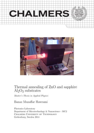
- 4. Thermal annealing of ZnO and sapphire Al2O3 substrates BANAZ MUZAFFAR HAWRAMI c BANAZ MUZAFFAR HAWRAMI ,2014 Photonics Laboratory Department of Microtechnology & Nanoscience - MC2 Chalmers University of Technology SE-412 96 G¨OTEBORG SWEDEN Telephone: +46 (0) 31-772 1000 Cover: Thermolyne high temperature furnace in MC2 cleanroom. Printed by Chalmers Reproservice, Chalmers University Of Technology G¨oteborg, Sweden 2014
- 5. To the memory of my father
- 7. Abstract ZnO is a compound semiconductor with a wide and direct bandgap of 3.3 eV which corresponds to UV light. This makes ZnO suitable for the violet-blue emitting opto- electronic devices. However, there are several challenges to obtain these devices. The substrate surfaces needs to be very smooth for epitaxial growth. This thesis focuses on the morphology of the Zn- and O-faces of ZnO and Al2O3 surfaces before and after thermal annealing. Several annealing parameters have been varied and the samples are analyzed by AFM and XRD. It turns out that for a high annealing temperature, the surface of Zn-face was improved. Atomic steps could observed on the surface. Smooth O-face surfaces were achieved at relatively low annealing temperatures. Sapphire is also a possible substrate for ZnO, it has also been investigated in this thesis.
- 9. Acknowledgment Initially, I would like to express my gratitude to my examiner Assoc. Prof. Tommy Ive for giving me an exciting opportunity to work on this interesting project. I am also thankful to him for his guidance and all discussions. Secondly, I would like to thank David Adolph for helping me with AFM, his remarkable assistance in the measurements, and for many helpful discussions. I could not get excellent results without his continuous help and mentorship. I would also like to thank Ulf S¨odervall and Christer Andersson for all the trainings in the cleanroom. I am grateful to Jan Andersson for the excellent IT support. Finally, I would like to thank my family, especially my beloved mother for her endless love and support and for giving me motivation to go ahead in life and excel in technologies of future. There are no words to express my gratitude to the one who is not with me anymore; I have finalized my thesis today is because of his inspiration and motivation. I just want to tell him:“I hope I’ve made you a happy and proud father today!’’ G¨oteborg Banaz M Hawrami September 2014
- 11. Contents 1 Introduction 1 1.1 Motivation . . . . . . . . . . . . . . . . . . . . . . . . . . . . . . . . . . . 1 2 Physical description 2 2.1 Introduction . . . . . . . . . . . . . . . . . . . . . . . . . . . . . . . . . . . 2 2.2 Crystalline properties of ZnO . . . . . . . . . . . . . . . . . . . . . . . . . 2 2.2.1 Bulk . . . . . . . . . . . . . . . . . . . . . . . . . . . . . . . . . . . 3 2.3 Crystalline properties of sapphire Al2O3 . . . . . . . . . . . . . . . . . . . 3 2.4 Smooth and rough surfaces . . . . . . . . . . . . . . . . . . . . . . . . . . 5 3 Experimental 7 3.1 pre-treatment . . . . . . . . . . . . . . . . . . . . . . . . . . . . . . . . . . 7 3.2 Characterization techniques . . . . . . . . . . . . . . . . . . . . . . . . . . 8 3.2.1 Atomic Force Microscopy AFM . . . . . . . . . . . . . . . . . . . . 8 3.2.2 X-ray Diffraction (XRD) . . . . . . . . . . . . . . . . . . . . . . . . 9 4 Measurement results and discussion 10 4.1 ZnO annealing . . . . . . . . . . . . . . . . . . . . . . . . . . . . . . . . . 10 4.1.1 Annealing with varying annealing times . . . . . . . . . . . . . . . 16 4.1.2 Annealing of ZnO with various annealing temperatures and an- nealing times . . . . . . . . . . . . . . . . . . . . . . . . . . . . . . 20 4.1.3 Methods . . . . . . . . . . . . . . . . . . . . . . . . . . . . . . . . . 27 4.2 Sapphire (Al2O3) annealing . . . . . . . . . . . . . . . . . . . . . . . . . . 27 4.3 XRD Results . . . . . . . . . . . . . . . . . . . . . . . . . . . . . . . . . . 35 5 Conclusions and future Work 38 References 43 i
- 12. 1 | Introduction ZnO is a direct wide gap material (Eg ∼ 3.3 eV at 300 K) in the UV-range. It also has a large exciton binding energy (60 meV). These unique properties make ZnO as a promising semiconductor for short-wavelength light-emitting devices. For production of these devices, ZnO substrates are advantageous. For homoepitaxy and heteroepitaxy smooth surfaces are required because rough surfaces can affect the electronic and optical properties. In order to improve the surface morphology, thermal annealing can be used. The improvement of the substrate is evaluated by means of atomic force microscopy (AFM), high resolution X-ray diffraction (XRD) and reflection high energy electron diffraction (RHEED). 1.1 Motivation By hydrothermal growth technique one can achieve high-quality sapphire Al2O3 and bulk ZnO substrates. However, the surfaces of these substrates are not smooth enough for epitaxial growth. For epitaxial growth, atomically flat surfaces are needed. There are several surface preparation techniques like wet treatment i chemical solutions and thermal annealing. The purpose of this thesis is to achieve smooth Al2O3 and ZnO surfaces for ZnO homoepitaxy by molecular beam epitaxy (MBE). 1
- 13. 2 | Physical description This chapter describes the crystalline properties of ZnO and sapphire Al2O3. Also, a review on polarity and polarization for ZnO is given. A description of two important concepts for this thesis, smooth and rough surfaces is given. 2.1 Introduction Depending on the ambient conditions, ZnO crystallizes in three different crystal struc- tures. They are wurtzite, zincblende and rocksalt. The most thermodynamically stable crystal structure is wurtzite structure [1]. 2.2 Crystalline properties of ZnO ZnO is a group II-VI compound semiconductor. It has wurtzite crystal structure( Fig- ures: 2.1 and 2.2). Each ion is bonded to four other ions. The surface atoms are bonded to three other atoms (Figure 2.1). Figure 2.1: Crystal struc- ture of ZnO [2]. Figure 2.2: Side views of Zn- polar (0001) direction and O-polar (000¯1) direction of a ZnO surface [2]. Some of the physical properties of ZnO such as lattice constants, melting point and energy bandgap are summarized in table 2.1. 2
- 14. 2.3. CRYSTALLINE PROPERTIES OF SAPPHIRE AL2O3 Table 2.1: Some of various properties of ZnO [3][1]. Property Value a (˚A) 3.25 c (˚A) 5.207 Melting point (◦C) 1975 Energy bandgap Eg(eV ) 3.3 2.2.1 Bulk For this thesis ZnO in both O-face and Zn-face with size 10 × 5 × 0.5 mm3 were used. The wafers were obtained from semiconductor wafer, inc. ( SWI) ( it is one of the largest semiconductor and electronic material supplier in Taiwan ) and prepared by the hydrothermal method. The surfaces were double side polished. ZnO is a transparent semiconductor and pure ZnO crystal is white. The color of ZnO becomes yellow during annealing by but reverts to white again after cooling. Figures 2.3 and 2.4 show Oxygen and Zinc faces of as-received wafers. Figure 2.3: O-face (000¯1) direc- tion of a ZnO substrate. Figure 2.4: Zn-face (0001) direc- tion of a ZnO substrate. 2.3 Crystalline properties of sapphire Al2O3 Sapphire Al2O3 has corundum crystalline structure, each aluminum atom is surrounded by six oxygen atoms. Sapphire is not a polar material and it has not a simple crystal structure like ZnO 2.5. 3
- 15. 2.3. CRYSTALLINE PROPERTIES OF SAPPHIRE AL2O3 Figure 2.5: Hexag- onal cell. (1) Alu- minum ions; (2) octahe- dral hollows[4]. . Figure 2.6: Scheme of the rhombohedron ele- mentary cell of sapphire Al2O3 [4]. Figure 2.7: The bond- ing between the hexag- onal and rhombohedral elementary cells: (1) octahedral hollows; (2) aluminum ions[4]. . In the crystal lattice of sapphire, two structural elementary cells hexagonal and rhombohedral can be found [4], see Figure 2.7 for en illustration. A schematic of the rhombohedron elementary cell and hcp of sapphire can be see in Figure 2.6. In Figure 2.5 oxygen atoms are stacked and form hexagonal close packed structure. Arrangement of octahedrons in the planes from axis C are different. Table 2.2: Some of various properties of Al2O3. Property Value a (˚A) 4.765 c (˚A) 12.982 Melting point (◦C) 2030 Energy bandgap Eg(eV ) 8.7 4
- 16. 2.4. SMOOTH AND ROUGH SURFACES 2.4 Smooth and rough surfaces In this subsection, a brief introduction on the theory behind the transition of a surface from rough by thermal annealing into smooth. This theory is based on a two-dimensional system. For a surface which is a two-dimensional system, the fundamental elements of the surface morphology such as terraces and steps are more easier to observe. For this thesis ZnO(000¯1) and ZnO(0001) are used which both have high-symmetry direction. To understand the transition of a surface from rough into smooth, some knowledge about the atom bonds on the surface is needed. Each surface in air ambient is oxygen-terminated. This is due to that the substrate is surrounded by the Oxygen atoms in the air and they bond to the dangling bonds of the atoms on the surface. As mentioned before, ZnO has the wurtzite crystal structure. On the Zn-face surface, each oxygen atom has three dangling bonds, wheres on the O-face surface it has only one dangling bond along the c-axis [5]. This makes the Zn-face more reactive than the O-face. This is possibly the reason why the Zn-face has less steps flat terraces on the surface than O-face after annealing. Polarity is a bulk property whereas face is a surface property [6]. Adatoms are the diffusing atoms on the surface during for instance MBE growth [7]. During annealing of ZnO and Al2O3 at high annealing temperature Zn , O and Al atoms evaporate from the surfaces because the forces between atoms in dangling bonds are weakened and the bonds are readily broken. In this thesis the adatoms are the evaporated atoms at high annealing temperatures. The theory behind annealing will be presented. Later from the AFM in chapter 4 are observed steps and terraces at low annealing temperatures on the O-face. Due to fewer dangling bonds, more freemoving adatoms can be found on the surface. These adatoms create the steps and flat terraces on the surface. A surface at a temperature TR undergoes a roughening transition as given by [7] : TR ≈ W1 kBln2 (2.1) Where W1 is the step energy per unit length in kelvin and kB is the Boltzmann constant. TR depends on the surface orientation [7] and the roughening transition temperatures are different for O-face and Zn-face. Pimpinelli and Villain [7] defined a surface as a rough surface if it’s height-height correlation function diverges. The height-height correlation function is given by: G(R) ≡< [z(r) − z(r + R)2 ] > (2.2) Let an infinite surface have a point (x,y,z), z is assumed to be height and one-valued function of x and y of the surface and R = (x,y) is defined as the two-dimensional space. If there is a divergence G(R): G(R) ≈ (4πkBT/σ)lnR (2.3) Where σ is the surface tension. A surface is smooth if there is no divergence. It is given by when (R = 0) : G(R) 2exp(−βWa) (2.4) 5
- 17. 2.4. SMOOTH AND ROUGH SURFACES Where Wa = 4W1 in a broken bond model for a cubic crystal and β = 1/kBT. This gives twice the adatom density at equilibrium according to the Gibbs formula: ρ = exp(−βWa) (2.5) 6
- 18. 3 | Experimental The first section in this chapter is describes the preparation of the ZnO substrates before annealing. After annealing of the surfaces, the substrates were characterized using AFM and X-ray diffraction. A brief descriptions for these techniques is subject for next section. 3.1 pre-treatment Before annealing of the surface, the wafer needed to be cleaned. In order to remove the organic contaminants from the surface, the samples were immersed for 7 minutes in aceton (OC(CH3)2). To remove the aceton solution on the samples, they were immersed for 7 minutes in isopropanolc and in the last step they were immersed for 7 minutes in deionized H2O. For efficient cleaning, ultrasonic treatment was employed in all three steps. Finally the samples were dried by N2. Figure 3.1: A photograph of the Temprese furnace used for dry ox- idation in the MC2 cleanroom. Figure 3.2: A Thermolyne furnace in MC2 cleanroom. 7
- 19. 3.2. CHARACTERIZATION TECHNIQUES 3.2 Characterization techniques The two characterization techniques used for this thesis, they will be discussed in this section. 3.2.1 Atomic Force Microscopy AFM AFM belong to scanning probe microscopy (SPM). By this technique, the surface of a sample is studied on an atomic level. The working principle for AFMM is a sharp probe that scans across the surface of samples at a distance of a few nanometers. There are three different modes of AFM, contact mode, non-contact mode and tapping mode. For this thesis tapping mode was used. In this mode the lateral forces are virtually eliminated since the cantilever is oscillated at or near its resonance frequency (200-400 kHz) with an amplitude ranging 20 nm to 10nm and a very sharp tip (with a radius < 10 nm) lightly “taps” on the sample surface during the scanning, contacting the surface at the bottom of its swing [8]. Figure 3.3: Schematic illustration of the principle of AFM.[8] Figure 3.4: The Bruker Dimension 3100 AFM in the MC2 cleanroom. Figure 3.3 shows the principle for AFM. A laser beam aims on the tip which scans along a surface. The reflection beam of the laser measures the tip’s deflection. In order to remain the tip deflection constant, The reflection beam is led into feedback loop which changes the surface height z. Data from the height z is used to form a (3D) topographic image of the surface. For measuring the surface roughness, the root mean square (RMS) is the most common measure. The RMS is a statistical value and a low RMS dose not mean a smooth surface always. This can be observed for the sapphire experiments 8
- 20. 3.2. CHARACTERIZATION TECHNIQUES results. Studying both the section of a surface and the RMS value gives a more correct assessment of the surface morphology. RMS or Rq is the standard deviation of the z values ( vertical movement of the tip) within a given area:[? ] RMS = N i=1(zi − zave)2 N (3.1) Where zave is a the average z value within a given area which contains N number of points, and zi is the current z value. 3.2.2 X-ray Diffraction (XRD) To obtain information on the semiconductor crystal structure XRD is used. X - ray diffraction is based on Bragg’s law: 2dsinθ = nλ (3.2) Where d is the distance between atomic planes and θ is the Bragg angle. Figure 3.5: Geometric illustration of an X-ray measure- ment showing sample and relevant angles for XRD.[8] Figure 3.6: XRD equip- ment in the MC2 cleanroom . As shown in the figure 3.5, ω is the angle between the specimen plane and the X-ray source beam. The 2θ is the angle between the reflected X-ray beam and the projected incoming beam. The sample can tilt parallel to specimen plane, the azimuthal rotation Φ and also around the perpendicular plan to the specimen Ψ. There are several different XRD measurements. The ω scan is used for gain information about the crystal quality by studying the full width half maximum (FWHM) of the diffraction peaks. Low crystal quality gives broader peaks. 9
- 21. 4 | Measurement results and dis- cussion In this chapter the experimental results are presented. Interesting results have been achieved for ZnO annealing investigation specially for zinc-terminated (0001) direction (zinc face), and may be published. The surface morphology was investigated by atomic force microscopy (AFM) and the crystalline quality by x-ray diffraction (XRD). 4.1 ZnO annealing Figure 4.1: AFM images (5×5 µm2 ) shows surface morphologies of a ZnO substrate before annealing (as-received) (a) Oxygen face and (b) Zinc face. Before epitaxial growth of ZnO, surface damages should be removed in order to achieve a very smooth surface. An as-received and rough ZnO surface is shown in figure 4.1. Damages and scratches on both faces of the ZnO wafer (figure 4.1 (a) and (b)) can be 10
- 22. 4.1. ZNO ANNEALING observed. High-temperature thermal treatment has been used both for oxygen and zinc faces to achieve smooth surfaces. By annealing of surfaces, three annealing parameters were investigated; annealing time (t), annealing temperature (T) and annealing ambient φo2 ). In air ambient, there was not any O2 flow. And for annealing in oxygen ambient, an O2 flow of 6 standard liters per minutes (slm) was on. From AFM images revealed that, the scratches on the surface were removed at temperature > 1050 ◦C and resulted in a flat surface with terraces and steps like features on both O- and Zn- faces. Figure 4.2 and figure 4.4 on page 14 shows, 5 × 5 µm2 AFM images for both oxygen and zinc faces for wide temperatures range from 950 ◦C to 1250 ◦C for one hour annealing time in flowing 6 slm oxygen gas. Figure 4.2: AFM images (5 × 5 µm2 ) of annealed ZnO surfaces under 6 liter per minute oxygen flow for ( a) O-face at 950 ◦ C, (b) O-face at 1000 ◦ C, (c) O-face at 1050 ◦ C, (d) O-face at 1100 ◦ C, (e) Zn-face at 950 ◦ C, (f) Zn-face at 1000 ◦ C, (g) Zn-face at 1050 ◦ C and (h) Zn-face at 1100 ◦ C. Table 4.1 include the AFM root mean square (RMS) values for O-face. And in table 4.2 on page 15 the results for annealing of Zn-face are collected. The surface annealing were made at different temperatures and different annealing times. Most of the surfaces were annealed with an O2-flow of 6 slm. And the rest in air ambient, which is mentioned in the tables. 11
- 23. 4.1. ZNO ANNEALING Table 4.1: Results for thermal annealing of O-face with various O2-flows. Annealing Temperature [◦C ] Annealing Time [hour/s] O2-flow [slm] AFM RMS Roughness [nm] 25 0 0 1.5000 950 1 6 0.3770 1000 1 6 0.4470 1050 1 6 0.4750 1050 6 6 0.1950 1100 1 6 0.4200 1100 3.5 6 0.9060 1100 3.5 0 0.2630 1100 5 6 0.2600 1115 4 6 0.2220 1150 1 6 0.1260 1150 3 6 0.1190 1165 1 0 0.2010 1200 1 6 0.3890 1240 1 6 0.1020 Figure 4.3 shows a plot of the RMS roughness versus annealing temperature for O- face with 6 liter per min oxygen flow. The surfaces were annealed for 1 hour. The green point shows RMS at 1165 ◦C without oxygen flow. The RMS roughness for an as-received O-face surface was 1.5 nm. A minimum RMS roughness of 0.102 nm was obtained at 1240 ◦C. 12
- 24. 4.1. ZNO ANNEALING Figure 4.3: Temperature dependence of RMS surface roughness (RMS∼T) for 1 hour annealed O-face in 6 liter per minute oxygen flow. The full green circle shows RMS at 1165 ◦ C without oxygen flow. The RMS decreased considerably by thermal annealing of surfaces from 1.5 nm to a minimum of 0.102 nm. In general, the RMS roughness decreases with increasing annealing temperature. 13
- 25. 4.1. ZNO ANNEALING Figure 4.4: AFM images (5 × 5 µm2 ) of ZnO surfaces annealed for 1 hour with under 6 liter per minute oxygen flow for (a) Zn-face at 1150 ◦ C,( b) Zn-face at 1200 ◦ C, (c) Zn-face at 1240 ◦ C, (d) Zn-face at 1250 ◦ C, (e) O-face at 1150 ◦ C, (f) O-face at 1200 ◦ C and (g) O-face at 1240 ◦ C. As it can be seen in the figures 4.4 that the surface morphology for Zn-face improved after annealing at 1100 ◦C and generates a well structured surface. Steps and terraces had developed on the surface. In general, for oxygen terminated face the steps are more developed and very well structured compared to zinc terminated face. This can be observed in the figures 4.2 and 4.4. 14
- 26. 4.1. ZNO ANNEALING Table 4.2: Results for thermal annealing of Zn-face with various O2-flow. Annealing Temperature [◦C ] Annealing Time [hour/s] O2-flow [slm] AFM RMS Roughness [nm] 25 0 0 1.5200 950 1 6 0.8510 1000 1 6 0.2070 1050 1 6 0.9260 1050 6 6 0.7900 1100 1 6 1.1000 1100 2.5 6 0.0699 1100 3.5 6 0.1010 1100 3.5 0 0.4210 1100 5 6 0.7730 1115 4 6 0.4230 1150 1 6 0.3390 1150 3 6 0.1310 1165 1 0 0.1200 1200 1 6 0.3980 1240 1 6 0.0877 1250 1 6 0.1260 The RMS decreased less for annealing of Zn-face compared to annealing of O-face. This leads to some difficulties to improve the surface quality for Zn-face and use for homoepitaxial growth. A plot of surface roughness for Zn-face for 1 hour annealing time is shown in figure 4.5. The minimum RMS achieved, is 0.0877 nm at 1240 ◦C with oxygen flow of 6 slm. 15
- 27. Figure 4.5: Temperature dependence of RMS surface roughness(RMS∼T) of the Zn-face. The annealing time was 1 hour and the oxygen flow 6 slm. The red point shows RMS at 1165 ◦ C in air ambient. The trend for Zn-face is similar to the O-face in that a higher annealing temperature results in a lower RMS roughness (Fig.4.5 ). It is uncertain if the oxygen flow improves the RMS values as compared to annealing in air ambient (no oxygen flow). 4.1.1 Annealing with varying annealing times In a series of experiments, the ZnO surface were annealed at 1100 ◦C while annealing time was changed. AFM images for both O-face and Zn-face, are shown in figure 4.6. Annealing of surfaces were made with an oxygen flow of 6 slm.
- 28. Figure 4.6: AFM images of annealed ZnO surfaces. The annealed temperature was 1100 ◦ C for (a) O-face 1 hour, (b) O-face 3.5 hours, (c) O-face 5 hours, (d) Zn-face 1 hour, (e) Zn-face 3.5 hours and (f) Zn-face 5 hours. Figure 4.7 shows a plot of RMS values versus annealing time for the O-face at a temperature of 1100 ◦C in oxygen flow of 6 slm. The result for one of the experiment in air ambient is also shown in the same graph. The blue point shows the RMS roughness for a 3.5 hours annealed surface. The comparison of the AFM images are shown in the figure 4.10 for annealed surfaces in air ambient and with an oxygen flow. From the graph and AFM images is found that the RMS value is less for O-face in air ambient, while conversely applies for the Zn-face(see figure 4.8).
- 29. Figure 4.7: RMS roughness values versus annealing time(RMS∼t) for an annealed O-face at 1100 ◦ C with an oxygen flow of 6 slm. The blue point shows the RMS roughness for annealed surface in air ambient.
- 30. Figure 4.8: RMS roughness values versus annealing time(RMS∼t) for an annealed Zn-face at 1100 ◦ C with an oxygen flow of 6 slm. The red point shows the RMS value for an annealed surface in air ambient. Figure 4.9: (a) AFM micrograph of the Zn-face of a ZnO substrate annealed at 1100 ◦ C for 2.5 hour. (b) Height variation along the line indicated in (a).
- 31. Figure 4.10: AFM images ( 5 × 5 µm2 ) of annealed ZnO surfaces at 1100 ◦ C for 3.5 hours for (a) O-face with an O-flow of 6 slm, (b) O-face in air ambient, (c) Zn-face with an O-flow of 6 slm and (d) Zn-face in air ambient. Further an experiment only for Zn-face was done at anneal temperature of 1100 ◦C for a 2.5-hour annealing time with an O-flow. The minimum RMS value was achieved for this point is 0.0699 nm. This is shown in figure 4.8. Figure 4.9 shows the variation of section height for this annealed surface. The section length is almost 1.8 µm. 4.1.2 Annealing of ZnO with various annealing temperatures and an- nealing times In another series of experiments, annealing of ZnO surfaces was made with various annealing times and annealing temperatures.The results in terms of surface morphology is shown in Fig: 4.11.
- 32. Figure 4.11: AFM images (5 × 5 µm2 ) of ZnO surfaces with an O-flow of 6 slm for (a) O-face at 1050 ◦ C for 6 hours, (b) O-face at 1115 ◦ C for 4 hours, (c) O-face at 1150 ◦ C for 3 hours, (d) Zn-face at 1050 ◦ C for 6 hours, (e) Zn-face at 1115 ◦ C for 4 hours and (f) Zn-face at 1150 ◦ C for 3 hours. The corresponding RMS values for the O-face results in figure 4.11 are plotted in figure 4.12. The surfaces have almost similar RMS. The step formation can be observed in Figs: 4.11(a)-(c). For O-face the steps developed easily and are more well structured. For Zn-face needs high annealing temperatures to obtain steps compare to O-face.
- 33. Figure 4.12: RMS surface roughness of annealed O-face surfaces for different temperatures and different annealing times. Figure 4.13 shows the RMS values of annealed Zn-face surfaces for different temper- atures and different annealing times. Lowest RMS roughness is achieved at an annealing temperatures of 1150 ◦C with an annealing time of 3 hours.
- 34. Figure 4.13: RMS surface roughness of annealed Zn-face surfaces for different temperatures and different annealing times. Substrates were also annealed at 1165 ◦C for 1 hour in air ambient. The surface morphologies for this samples are shown in the figure 4.14.
- 35. Figure 4.14: AFM images ( 5 × 5 µm2 ) of ZnO surfaces for an annealing temperatures of 1165 ◦ C with an annealing time of 1 hour (a) O-face and (b) Zn-face. In this subsection, the section height variation are presented for as-received, indiffer- ent and best achieved surface roughness after thermal annealing.
- 36. Figure 4.15: AFM section height (a) O-face before annealing ( as-received state) and (b) Zn-face before annealing ( as-received state) Zn-face after a 6 min cleaning degreasing procedure. Figures 4.15 shows the surface morphologies and height variations for both O-face and Zn-face for an as-recieved substrate.In Figure 4.16 (c) and (d) shows the smoothest surface for O and Zn-faces after thermal annealing. As can be seen in this figures, the surface features and graphs are significantly different from as-received surface ( 4.15). The non-annealed surfaces were much rougher with an RMS value ∼ 1.5 nm for both faces as compared to the best achieved smoothness with an RMS ∼ 0.1 for both faces. For the smooth surfaces terraces and steps can be observed. By studying AFM scan sections on these surfaces, the step height and width can be obtained. These are presented in the graphs ( Figs 4.16).
- 37. Figure 4.16: AFM images ( 5 × 5 µm2 ) and section height (a) annealed O-face at 1050 ◦ C for 1 hour annealing time, (b) annealed Zn-face at 1100 ◦ C for 1 hour annealing time, (c) annealed O-face at 1100 ◦ C for 5hours annealing time and (d) annealed Zn-face at 1240 ◦ C for 1 hour annealing time.
- 38. 4.1.3 Methods The O-face surfaces at temperature 1100 ◦C undergo a transition from a rough surface to a flat surface with terraces. From expression 2.1, the step energy per unit length is given by: W1 ≈ TRkBln2 (4.1) According to this expression, the step energy per unit length for the O-face at tem- perature 1373 kelvin is 1.31 × 10²⁰ Kelvin. The adatoms energy for the wurtzite crystal structure can be approximated for a cubic crystal to Wa = 4W1. Using the expression 4.1 into Gibbs expression 2.5, the adatoms density at equilibrium yields: ρ = exp(− 4TRln2 T ) (4.2) From this expression the adatoms density for O-face at equilibrium is: 2.2415 × 10⁻⁹. For Zn-face surfaces at temperature 1240 ◦C the steps could be observed. For this tem- perature the step energy per unit length from expression is 4.1 is 1.44 × 10⁻²⁰kelvin. This gives the adatoms density for Zn-face about 3.46 × 10⁻⁹ at equilibrium. The O- face surface adatom density is almost 6.5 times greater than the Zn-face surface adatom density. 4.2 Sapphire (Al2O3) annealing In this section the results for experimental investigation of sapphire annealing are pre- sented. Annealing of sapphire started with temperature > 1400◦C . Later we realized that by decreasing temperature, smoother surface could be achieved . Figure 4.17: AFM image of an as-received sapphire substrate surface.
- 39. Table 4.3: Results from the thermal annealing of sapphire Al2O3 substrates in air ambient. Annealing Temperature [◦C ] Annealing Time [hour/s] O2-flow [slm] AFM RMS Roughness [nm] as-received 0 0 0.0528 1200 1 0 0.0544 1200 1 6 0.0692 1250 2 0 0.0688 1250 2 6 0.0582 1400 2 0 0.0834 1450 1 0 0.1240 1450 2 0 0.1130 1475 1 0 0.2360 1500 1 0 0.1570 1550 1 0 0.7060 For annealing of the sapphire substrates, high temperature furnaces were used. Most of the surfaces were annealed in air ambient 4.18. All experimental results are listed in table 4.3.
- 40. Figure 4.18: AFM images ( 5 × 5 µm2 ) of sapphire surfaces in air and oxygen ambient annealed at (a) 1200 ◦ C for 1 hour in air ambient, (b) 1200 ◦ C for 1 hour with an O-flow of 6 slm, (c)1450 ◦ C for 1 hour in air ambient, (d) 1574 ◦ C for 1 hour in air ambient, (e) 1250 ◦ C for 2 hours in air ambient, (f) at 1250 ◦ C for 2 hours with an O-flow of 6 slm, (g) 1400 ◦ C for 2 hours in air ambient, (h) 1450 ◦ C for 2 hours in air ambient, Figure 4.19 shows two more annealed surfaces. The surface morphology was not improved by increasing temperature. For a surface annealed at 1550 ◦C white spots can be observed. These are AFM artifacts.
- 41. Figure 4.19: AFM images of anneald sapphire surface in air ambient at (a)1500 ◦ C for 1 hour and (b)1550 ◦ C for 1 hour. The RMS roughness obtained by AFM for 1-hour annealed surfaces in air ambient is plotted in figure 4.20. The star point shows the RMS for a 2-hour annealed surface at annealing temperature 1250 ◦C. This point is also the minimum RMS. The RMS is a statistical measure of surface smoothness. A small RMS means that the surface is smoother statistically. The surface morphology is not improved by low RMS cause the RMS is not equal to surface morphology
- 42. Figure 4.20: AFM RMS versus annealing temperature for a 1-hour annealed surfaces in air ambient. The star point shows RMS for annealed surface with an O-flow of 6 slm. Figure 4.21 showsthe results for annealed surfaces for 2 hours. There are two more points that indicate annealing in various conditions. The star point shows RMS for a 2-hour annealed surface with an O-flow of 6 slm. This point is the minimum RMS for these series of experiments. The circle indicate RMS surface roughness for a 1-hour annealed surface in air ambient.
- 43. Figure 4.21: AFM RMS versus annealing temperature for a 2-hour annealed surfaces in air ambient. The star point is for a 2-hour annealed surface with an O-flow of 6 slm. The circle is for 1-hour annealed surface in air ambient. The AMF section height variation for all annealed surfaces is presented in figures 4.22, 4.23 and 4.24. There is no step on an as-received surface (see figure 4.22 (a)). Thermal annealing also resulted in step morphology on sapphire surfaces. The step height variations for annealed surfaces depend on annealing conditions such as annealing time, annealing atmosphere and annealing temperature.
- 44. Figure 4.22: AFM 5×5 µm2 images and section height for Al2O3 substrate surfaces for (a) as-received surface, (b) annealed surface at 1450 ◦ C for 1 hour in air ambient, (c) a 1- hour annealed surface at 1500 ◦ C in air ambient and (d) a 1-hour annealed surface at 1500 ◦ C in air ambeint.
- 45. Figure 4.23: AFM 5 × 5 µm2 images and section height for Al2O3 substrate surfaces for (a) annealed surface at 1200 ◦ C for 1 hour in air ambient, (b) annealed surface at 1200 ◦ C for 1 hour with an O-flow of 6 liter per min, (c) annealed surface at 1250 ◦ C for 1 hour with an O-flow of 6 slm and (d) annealed surface at 1250 ◦ C for 2 hour in air ambient.
- 46. Figure 4.24: AFM 5 × 5 µm2 images and section height for Al2O3 substrate surfaces for (a) annealed surface at 1450 ◦ C for 1 hour in air ambience (b) annealed surface at 1475 ◦ C for 2 hours in air ambience and (c) annealed surface at 1400 ◦ C for 2 hours in air ambience. 4.3 XRD Results In this subsection the crystalline quality for zinc-terminated ZnO is investigated for two annealed substrates and compared to an as-received substrate. By observing the full width at half maximum (FWHM) of x-ray rocking curve ( XRC) we see diffraction
- 47. peaks. And get information about the crystalline quality. In general, a narrow FWHM indicates a high crystal quality. The substrates were annealed for 1 hour at 1200 ◦C and 1240 ◦C. The XRD results are listed in table 4.4. Table 4.4: XRD results for 1 hour thermal annealed Zn-face with 6 liter per min O2 flows at two different temperatures and for an as-received Zn-face. Annealing Temperature [◦C ] Annealing Time [hour] O2-flow [slm] AFM RMS Roughness [nm] FWHM [deg] as-received 0 0 0.00710 1200 1 6 0.01311 1240 1 6 0.00815 Figure 4.25: XRC of the (0002) reflection from an as-received Zinc face. Figure 4.26: XRC of the (0002) reflection from a 1 hour annealed Znic face at 1200 ◦ C with 6 liter min oxygen.
- 48. Figure 4.27: XRC of the (0002) reflection from a 1 hour annealed Znic face at 1240 ◦ C with 6 liter min oxygen. Figure 4.28: Normalized diffracted inten- sity versus incident angle for all 3 samples compare to the logarithmic normalized .
- 49. 5 | Conclusions and future Work ZnO substrate were annealed at temperatures 950 ◦C up to 1250 ◦C under various an- nealing time and O2-flow. We achieved smooth O-face surfaces at relatively lower tem- peratures compare to Zn-face surfaces. We observed the steps on O-face after annealing at 1100 ◦C with an O2-flow of 6 slm and scratches with depth of 3 nm were removed. After 5 hours at 1100 ◦C annealing in a 6 slm flowing O2 ambient a step with length of .173 µm and height of 4.59 ˚A was obtained. The C axis of ZnO is 5.2˚A. This means we preformed the O-face surface and achieved a steps with length less than C-axis. For preforming of Zn-face surface needs high temperatures. The scratches on Zn-face had a dept of almost 4nm. The smoothest achieved Zn-face was a surface after 1 hours at 1240 ◦C annealing temperature in a 6 slm flowing O2. This surface contain a step with length 0.1µm and a step height with 400 pm. This performance of the Zn-face is significant , the hight is less than C-axis. We removed almost 9 layers of C-axis. The investigation of crystal quality by XRD shows that the crystalline quality does not change after annealing and changing of surface morphology. Sapphire substrate were annealed at temperatures 1200 ◦C up to 1550 ◦C under vari- ous annealing time and O2-flow. It shows that surface morphology becomes progressively worse for higher temperatures. After 2 hours at 1250 ◦C annealing temperature in a 6 slm flowing O2 we obtained a step with length .1µm and with a step height of 150 pm. The steps developed easily and for sapphire substrates. The RMS value for AFM mea- surements are studying too, but the results are presented by studying the AFM section variation of the surfaces. The RMS is the statistical measure of the surface smoothness, A surface with low RMS is not always smoothest. For instance, an unannealed sapphire substrate has RMS value of 0.0528 the smoothest achieved surface has almost the same RMS ( 0.0582). This process can be apply on MBE growth substrates. The investigation of surface morphology for this substrate for various annealing temperature and different annealing conditions ca be done in future. 38
- 50. Bibliography [1] N. Izyumskaya, V. Avrutin, . ¨Ozg¨ur, Y. I. Alivov, H. Morko¸c, Preparation and properties of zno and devices, physica status solidi (b) 244 (5) (2007) 1439–1450. URL http://dx.doi.org/10.1002/pssb.200675101 [2] J. G¨otzen, G. Witte, Rapid preparation of highly ordered ultraflat zno surfaces, Applied Surface Science 258 (24) (2012) 10144 – 10147. URL http://www.sciencedirect.com/science/article/pii/ S0169433212011579 [3] A. Kobayashi, J. Ohta, H. Fujioka, Characteristics of single crystal zno annealed in a ceramic zno box and its application for epitaxial growth of gan, Japanese Journal of Applied Physics 45 (7R) (2006) 5724. URL http://stacks.iop.org/1347-4065/45/i=7R/a=5724 [4] softpedia, About: sapphire crystal structure, http://www.pmoptics.com/ sapphire.html, last checked: 2014-07-22 (2014). [5] H. Morkoc, U. Ozgur, Zinc Oxide Fundamentals, Materials and Device Technology, Willy-CCH, 2009. [6] D. Adolph, Growth of zno on gan by molecular beam epitaxy, Ph.D. thesis, Chalmers University of Technology (2014). [7] A. Pimpinelli, J. Villain, Physics of Crystal Growth, Cambridge University Press, 1998. [8] M. Cho, C. Harada, H. Suzuki, T. Minegishi, T. Yao, H. Ko, K. Maeda, I. Nikura, Issues in zno homoepitaxy, Superlattices and Microstructures 38 (4ˆa“6) (2005) 349 – 363, e-MRS 2005 Symposium G: ZnO and Related Materials Part 1 2005 European Materials Research Society Spring Meeting. URL http://www.sciencedirect.com/science/article/pii/ S0749603605000959 [9] A. Kobayashi, S. Kawano, Y. Kawaguchi, J. Ohta, H. Fujioka, Room temperature epitaxial growth of m-plane gan on lattice-matched zno substrates, Applied Physics Letters 90 (4) (2007) 041908–041908–3. 39
- 51. [10] A. Kobayashi, J. Ohta, H. Fujioka, Low temperature epitaxial growth of in0.25ga0.75n on lattice-matched zno by pulsed laser deposition, Journal of Ap- plied Physics 99 (12) (2006) –. URL http://scitation.aip.org/content/aip/journal/jap/99/12/10.1063/ 1.2206883 [11] X. Gu, M. A. Reshchikov, A. Teke, D. Johnstone, H. Morko¸c, B. Nemeth, J. Nause, Gan epitaxy on thermally treated c-plane bulk zno substrates with o and zn faces, Applied Physics Letters 84 (13) (2004) 2268–2270. URL http://scitation.aip.org/content/aip/journal/apl/84/13/10.1063/ 1.1690469 [12] S. Graubner, C. Neumann, N. Volbers, B. Meyer, J. Blasing, A. Krost, Preparation of zno substrates for epitaxy: Structural, surface, and electrical properties, Applied Physics Letters 90 (4) (2007) 042103–042103–3. [13] J.-M. Chauveau, M. Teisseire, H. Kim-Chauveau, C. Deparis, C. Morhain, B. Vinter, Benefits of homoepitaxy on the properties of nonpolar (zn,mg)o/zno quantum wells on a-plane zno substrates, Applied Physics Letters 97 (8) (2010) –. URL http://scitation.aip.org/content/aip/journal/apl/97/8/10.1063/1. 3481078 [14] J. Heffelfinger, M. Bench, C. Carter, Steps and the structure of the (0001) -alumina surface, Surface Science 370 (1) (1997) L168 – L172. URL http://www.sciencedirect.com/science/article/pii/ S0039602896011235 [15] J. R. Heffelfinger, C. Carter, Mechanisms of surface faceting and coarsening, Surface Science 389 (1–3) (1997) 188 – 200. URL http://www.sciencedirect.com/science/article/pii/ S0039602897004111 [16] D. Croxall, R. Ward, C. Wallace, R. Kell, Hydrothermal growth and investigation of li-doped zinc oxide crystals of high purity and perfection, Journal of Crystal Growth 22 (2) (1974) 117 – 124. URL http://www.sciencedirect.com/science/article/pii/ 0022024874901286 [17] L. N. Demianets, A. N. Lobachev, Hydrothermal synthesis of crystals, Kristall und Technik 14 (5) (1979) 509–525. URL http://dx.doi.org/10.1002/crat.19790140503 [18] H. Wang, J. Xie, K. Yan, M. Duan, Growth mechanism of different morphologies of zno crystals prepared by hydrothermal method, Journal of Materials Science Technology 27 (2) (2011) 153 – 158. URL http://www.sciencedirect.com/science/article/pii/ S1005030211600418
- 52. [19] T. Sekiguchi, S. Miyashita, K. Obara, T. Shishido, N. Sakagami, Hydrothermal growth of zno single crystals and their optical characterization, Journal of Crystal Growth 214–215 (0) (2000) 72 – 76. URL http://www.sciencedirect.com/science/article/pii/ S0022024800000658 [20] D. Ehrentraut, K. Maeda, M. Kano, K. Fujii, T. Fukuda, Next-generation hy- drothermal zno crystals, Journal of Crystal Growth 320 (1) (2011) 18 – 22. URL http://www.sciencedirect.com/science/article/pii/ S0022024811000121 [21] W. Lim, V. Craciun, K. Siebein, B. Gila, D. Norton, S. Pearton, F. Ren, Surface and bulk thermal annealing effects on zno crystals, Applied Surface Science 254 (8) (2008) 2396 – 2400. URL http://www.sciencedirect.com/science/article/pii/ S0169433207013529 [22] H. Wu, M. Xue, J. Ou, F. Wang, W. Li, Effect of annealing temperature on surface morphology and work function of zno nanorod arrays, Journal of Alloys and Compounds 565 (0) (2013) 85 – 89. URL http://www.sciencedirect.com/science/article/pii/ S0925838813005148 [23] K. Grasza, E. Lusakowska, P. Skupinski, H. Sakowska, A. Mycielski, Thermal an- nealing of ZnO substrates, Superlattices and Microstructures 42 (1-6) (2007) 290– 293. URL http://dx.doi.org/10.1016/j.spmi.2007.04.066 [24] W. Mtangi, F. D. Auret, M. Diale, W. E. Meyer, A. Chawanda, H. de Meyer, P. J. Janse van Rensburg, J. M. Nel, Effects of high temperature annealing on single crystal zno and zno devices, Journal of Applied Physics 111 (8) (2012) –. URL http://scitation.aip.org/content/aip/journal/jap/111/8/10.1063/ 1.3700186 [25] Y. Gan, E. J. Wanless, G. V. Franks, Lattice-resolution imaging of the sapphire (0xa0;0xa0;0xa0;1) surface in air by {AFM}, Surface Science 601 (4) (2007) 1064 – 1071. URL http://www.sciencedirect.com/science/article/pii/ S0039602806012283 [26] K. Saw, Surface reconstruction of -(0001) sapphire: An afm, xps, aes and eels investigation, Journal of Materials Science 39 (8) (2004) 2911–2914. URL http://dx.doi.org/10.1023/B%3AJMSC.0000021479.20164.f8 [27] D. Zhang, Y. Gan, Effects of plasma treatment on evolution of surface step-terrace structure of critically cleaned c-plane sapphire substrates: An {AFM} study,
- 53. Applied Surface Science 285, Part B (0) (2013) 211 – 214. URL http://www.sciencedirect.com/science/article/pii/ S0169433213015262 [28] Y. Wang, S. Wang, S. Zhou, J. Xu, J. Ye, S. Gu, R. Zhang, Q. Ren, Effects of sapphire substrate annealing on zno epitaxial films grown by {MOCVD}, Applied Surface Science 253 (4) (2006) 1745 – 1747. URL http://www.sciencedirect.com/science/article/pii/ S0169433206002583 [29] X. Wu, B. Huang, H. Zhan, J. Kang, Properties of zno grown on sapphire with different buffer layers, Journal of Crystal Growth 318 (1) (2011) 519 – 523, the 16th International Conference on Crystal Growth (ICCG16)/The 14th International Conference on Vapor Growth and Epitaxy (ICVGE14). URL http://www.sciencedirect.com/science/article/pii/ S0022024810007712 [30] X. Li, J. Song, Y. Liu, H. Zeng, Controlling oxygen vacancies and properties of zno, Current Applied Physics 14 (3) (2014) 521 – 527. URL http://www.sciencedirect.com/science/article/pii/ S1567173914000108 [31] L. Irimpan, D. Ambika, V. Kumar, V. P. N. Nampoori, P. Radhakrishnan, Effect of annealing on the spectral and nonlinear optical characteristics of thin films of nano-zno, Journal of Applied Physics 104 (3) (2008) –. URL http://scitation.aip.org/content/aip/journal/jap/104/3/10.1063/ 1.2949400 [32] A. Zendehnam, M. Mirzaee, S. Miri, Effect of annealing temperature on {PL} spectrum and surface morphology of zinc oxide thin films, Applied Surface Science 270 (0) (2013) 163 – 168. URL http://www.sciencedirect.com/science/article/pii/ S0169433212023197 [33] S. Das, K. Dutta, A. Pramanik, Morphology control of zno with citrate: a time and concentration dependent mechanistic insight, CrystEngComm 15 (2013) 6349–6358. URL http://dx.doi.org/10.1039/C3CE40822A [34] T. Hashimoto, Y. Terakoshi, M. Ishida, M. Yuri, O. Imafuji, T. Sugino, A. Yoshikawa, K. Itoh, Structural investigation of sapphire surface after nitrida- tion, Journal of Crystal Growth 189–190 (0) (1998) 254 – 258. URL http://www.sciencedirect.com/science/article/pii/ S0022024898002553 [35] ¨U. ¨Ozg¨ur, Y. I. Alivov, C. Liu, A. Teke, M. A. Reshchikov, S. Do˘gan, V. Avrutin, S.-J. Cho, H. Morko¸c, A comprehensive review of zno materials and devices, Journal
- 54. of Applied Physics 98 (4) (2005) –. URL http://scitation.aip.org/content/aip/journal/jap/98/4/10.1063/1. 1992666 [36] A. Kobayashi, Y. Kawaguchi, J. Ohta, H. Fujioka, K. Fujiwara, A. Ishii, Polarity control of gan grown on zno (0001) surfaces, Applied Physics Letters 88 (18) (2006) –. URL http://scitation.aip.org/content/aip/journal/apl/88/18/10.1063/ 1.2200157 [37] F. F¨alth, Growth, characterization and processing of III-nitride semiconductors, Ph.D. thesis, Chalmers University of Technology (2005). [38] M. Ohring, Materials Science Of Thin Films Deposition and Structure, Academic Press, 2002. [39] news.softpedia.com, About: sapphire crystal1 structure, http://chemistry. stackexchange.com/questions/9730/why-dont-molecules-of-ionic- compounds-exist, last checked: 2014-09-04 (2014).