
Empfohlen
Empfohlen
Weitere ähnliche Inhalte
Was ist angesagt?
Was ist angesagt? (19)
Ähnlich wie Datasheet Layout for Semiconductor Companies
Ähnlich wie Datasheet Layout for Semiconductor Companies (20)
Kürzlich hochgeladen
Kürzlich hochgeladen (20)
Datasheet Layout for Semiconductor Companies
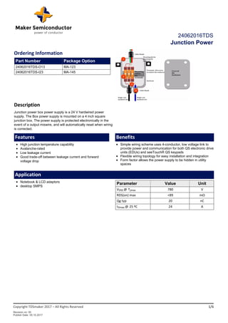
- 1. 24062016TDS Junction Power Ordering Information Part Number Package Option 24062016TDS-O13 MA-123 24062016TDS-I23 MA-145 Description Junction power box power supply is a 24 V hardwired power supply. The Box power supply is mounted on a 4 inch square junction box. The power supply is protected electronically in the event of a output miswire, and will automatically reset when wiring is corrected. Features High junction temperature capability Avalanche-rated Low leakage current Good trade-off between leakage current and forward voltage drop Benefits Simple wiring scheme uses 4-conductor, low voltage link to provide power and communication for both QS electronic drive units (EDUs) and seeTouchR QS keypads Flexible wiring topology for easy installation and integration Form factor allows the power supply to be hidden in utility spaces Application Notebook & LCD adaptors desktop SMPS Parameter Value Unit V @ TDSS jmax 780 V RDS(on) max <89 mΩ Qg typ 20 nC I @ 25 ºCDmax 24 A Copyright TDSmaker 2017 – All Rights Reserved 1/6 Revision no: 00 Publish Date: 05.10.2017
- 2. 24062016TDS Junction Power 1. Maximum Ratings Table 2 Maximum Ratings @ T = 25 ºC, unless otherwise specifiedj Parameter Symbol Values Unit Condition Min Typ Max Continuous drain current ID -14 10.5 A TC= 100ºC -19 12.4 A TC = 25ºC Pulsed drain current ID, pulse -30 19.5 A TC = 25ºC Avalanche energy, single pulse EAS -14 10.0 mJ I = 5.1A; V = 50V, VGS = 10V, L=10mH, RG=25 Ohms D DD Avalanche energy, repetitive EAR -14 20.0 mJ I = 2.0; V = 50VD DD Avalanche current, single pulse IAS 4 0.55 15.6 mJ - MOSFET dv/dt ruggedness dv/dt 10 4.1 A VDS = 0….480V Gate source voltage (static) VGS -14 10 V/ns Static Gate source voltage (dynamic) VGS -30 0.6 20 V AC (F>1Hz) Power dissipation Ptot -30 22 V TO-220, TO-263, TC = 25ºC Storage temperature Tstg -30 34.5 W - Operating junction temperature Tj -12 17 ºC - Mounting torque - 15 3.4 19 ºC M3 and M3.5 screws Continuous diode forward current ISD -30 45 N-cm Tc = 25ºC Diode pulse current IS, pulse -10 19 A Tc = 25ºC Reverse diode dv/dt -10 15 A V =0…480V, I <=I , T = 25ºCDS SD S j Maximum diode commutation speed di /dtf -10 11 V/ns V =0…480V, I <=I , T = 25ºCDS SD S j 2. Thermal Characteristics Table 3 Thermal Characteristics Symbol Parameter Values Unit MA-123 MA-145 MA-113 MA-432 Rth-jC Thermal resistance, junction-case 1.4 1.3 1.4 1.1 ºC W/ Rth-jA Thermal resistance, junction-ambient 70 70 70 70 ºC W/ TS Soldering temperature, wave soldering only allowed at leads 340 330 400 250 ºC Copyright TDSmaker 2017 – All Rights Reserved 2/6 Revision no: 00 Publish Date: 05.10.2017
- 3. 24062016TDS Junction Power 3. Electrical Characteristics Table 4 Static Characteristics @ T = 25ºC, unless otherwise specifiedj Parameter Symbol Values Unit Condition Min Typ Max Drain-source breakdown voltage V(BR)DSS 650 900 V I = 1mA, V = 0VD GS Gate threshold voltage VGS(TH) 2.5 2.7 2.9 V V = V I = 72uADS GS, D Zero gate voltage drain current IDSS - - 4 µA V = 650V, T = 25ºC, V = 0VDS C GS - - 100 V = 650V, T = 125ºC, V = 0VDS C GS Gate-source leakage current IGSS - - 100 mJ V = ±30V, V = 0VGS DS Drain-source on-state resistance RDS(on) - - 0.23 A V = 10V, I = 5.8 A, T = 25ºC GS D J Gate resistance RG - - 0.3 V/ns - Table 5 Dynamic Characteristics Parameter Symbol Values Unit Condition Min Typ Max Input capacitance Ciss - 1900 - pF V = 100V, f = 1MHz, V = 0V DS GS Output capacitance Coss - 56 - pF Reverse transfer capacitance Crss - 8 - pF Turn-on delay time td(on) - 4 - ns V = 400V, I = 4.5A R = 3.4Ω, V = 13V DD D G GS Rise time tr - 5 - ns Turn-off delay time td(off) - 3 - ns Fall time tf - 1 - ns Table 6 Gate Charge Characteristics Parameter Symbol Values Unit Condition Min Typ Max Gate to source charge Qgs 0,6 nC V = 480V, I = 5.8A, V = 0 to 10V DD D GS Gate to drain charge Qgd 34 nC Gate charge total Qg 3 nC Gate plateau voltage td(on) 0.8 V Table 7 Reverse Diode Characteristics Parameter Symbol Values Unit Condition Min Typ Max Diode source-drain current ISD 5 A Diode forward voltage Vfd 56 V I = 11.6A, V = 0V, T = 25ºC SD GS J Reverse recovery time trr 3 nS I = 11.6A, L = 5mH di/dt = 100A/µS V = 60V, T = 25ºC F DD J Reverse recovery charge Qrr 1.4 µC Peak reverse recovery current Irrm A Copyright TDSmaker 2017 – All Rights Reserved 3/6 Revision no: 00 Publish Date: 05.10.2017
- 4. 24062016TDS Junction Power 4. Electrical Characteristics Graphs Power Dissipation Maximum Transient Thermal Impedance Max power limited by case temperature Variable is pulse time (t )p Table 8 Thermal Performance Typical Output Characteristics Maximum Transient Thermal Impedance T = 25 C; Variable is VC o GS T = 125 C; Variable is VC o GS Table 9 Output Characteristics Typical Output Characteristics Maximum Transient Thermal Impedance T = 25 C; Variable is VC o GS T = 125 C; Variable is VC o GS Copyright TDSmaker 2017 – All Rights Reserved 4/6 Revision no: 00 Publish Date: 05.10.2017
- 5. 24062016TDS Junction Power Table 10 Drain-Source Resistance Typical Drain-Source On-State Resistance Drain-Source On-State Resistance Tj = 25oC; Variable is gate voltage (VGS) I = 14.3A, V =10VD GS Table 11 Safe Operating Area Typical Capacitances Typical Gate Charge V = 0V; Freq. = 1MHzGS I = 8.6A Pulsed Vdd = 480VD Copyright TDSmaker 2017 – All Rights Reserved 5/6 Revision no: 00 Publish Date: 05.10.2017
- 6. 24062016TDS Junction Power 5. Disclaim The information in this document is provided solely regarding TDSmaker products. The information is not a guarantee of performance or characteristics. TDSmaker reserves the right to modify, change, amend, improve or make corrections to this document, and its products, at any time and its sole discretion without prior written consent or notice. No license to any intellectual property rights is granted or implied under this document. TDSmaker disclaims warranties and liabilities of any kind including non-infringement of intellectual property rights of any third party. TDSmaker products may be used in applications such as automotive, military, aerospace, medical or other applications where failure or malfunction may result in personal injury, death or severe property or environmental damage only with express written approval from TDSmaker. Sale of TDSmaker products are subject toTDSmaker’s standard terms and conditions. Products not purchased through TDSmaker’sauthorized distributors, agents or sales representatives are void of warranty. Copyright TDSmaker 2017 – All Rights Reserved 6/6 Revision no: 00 Publish Date: 05.10.2017