SlideShare ist ein Scribd-Unternehmen logo
1 von 74
What is a DSP?
A specialized microprocessor for real-time DSP applications
Digital filtering (FIR and IIR)
FFT
Convolution, Matrix Multiplication etc
ADC DAC
DSP
ANALOG
INPUT
ANALOG
OUTPUT
DIGITAL
INPUT
DIGITAL
OUTPUT
Hardware used in DSP
ASIC FPGA GPP DSP
Performance Very High High Medium Medium High
Flexibility Very low High High High
Power
consumption
Very low low Medium Low Medium
Development
Time
Long Medium Short Short
Common DSP features
• Harvard architecture
• Dedicated single-cycle Multiply-Accumulate (MAC) instruction (hardware
MAC units)
• Single-Instruction Multiple Data (SIMD) Very Large Instruction Word
(VLIW) architecture
• Pipelining
• Saturation arithmetic
• Zero overhead looping
• Hardware circular addressing
• Cache
• DMA
INTRODUCTION
In a normal computer that follows von Neumann architecture,
instructions and data both are stored in same memory.
So same buses are used to fetch instructions and data. This means CPU
cannot do both things together (read a instruction and read/write data).
Harvard Architecture is the computer architecture that contains
separate storage and separate buses (signal path) for instruction and
data.
It was basically developed to overcome the bottleneck of Von Neumann
Architecture.
The main advantage of having separate buses for instruction and data is
that CPU can access instructions and read/write data at the same time.
Harvard Architecture
Physically separate
memories and paths
for instruction and
data
DATA
MEMORY
PROGRAM
MEMORY
CPU
STRUCTURE OF HARVARD ARCHITECTURE
BUSES
 Buses are used as signal pathways. In Harvard architecture there are separate
buses for both instruction and data. Types of Buses:
 Data Bus: It carries data among the main memory system, processor and I/O
devices.
 Data Address Bus: It carries the address of data from processor to main
memory system.
 Instruction Bus: It carries instructions among the main memory system,
processor and I/O devices.
 Instruction Address Bus: It carries the address of instructions from processor
to main memory system.
Operational registers
There are different types of registers
involved in it which are used for storing
address of different types of instructions.
For example, Memory Address Register
and Memory Data Register are operational
registers.
ProgramCounter
It has the location of the next
instruction to be executed. Program
counter then passes this next
address to memory address register.
Arithmetic and Logic Unit
Arithmetic logic unit is that part of the
CPU that operates all the calculations
needed. It performs addition, subtraction,
comparison, logical Operations, bit
Shifting Operations and various
arithmetic operations.
Control unit
Control unit the part of CPU that
operates all processor control
signals. It controls the input and
output devices and also control the
movement of instructions and data
within the system.
Input/output system
 Input devices are used to read data into main memory with the help of CPU
input instruction.
 The information from a computer as output are given through Output
devices.
 Computer gives the results of computation with the help of output devices.
ADVANTAGES
 Since data and instructions are stored in separate buses there are very few
chances of corruption.
 Data that uses Read-Only mode and instructions which uses Read-Write
mode are operated in the same way. They can also be accessed similarly.
 Generally, two memories would be present, one for data and the other one for
instructions, they have different cell sizes making use of the resources very
effectively.
 The bandwidth that is used for memory is more predictable.
 They generally offer high performance as data and buses are kept in separate
memory and travel on different buses.
 Parallel access to data and instructions can be maintained.
 Scheduling would no longer be required as there are separate buses for data
and instructions.
 Programmers can design the memory unit according to their requirements.
 Control unit gets data and instructions from one memory. Thus, it simplifies
the architecture of the control unit.
disadvantages
 The un-occupied data memory cannot be used by instructions and the free instruction
memory cannot be used by data. Memory dedicated to each unit has to be balanced carefully.
 The program cannot be written by the machine on its own as in Von Neumann Architecture.
 Control Unit takes more time to develop and is on the expensive side.
 There are 2 buses on the architecture. Which in the way means that the motherboard would
be more complex, which in turn means that there would be two RAMs and thus tends to have
a very complex cache design. That is the reason for it being used mostly inside the CPU and
not outside of it.
 Production of computer with 2 buses takes more time to get manufactured and is again on the
expensive side like the control unit.
 It has more pins on its IC’s. Therefore, it is very difficult to implement it.
 It is not used widely, so the development of it would be on the backward edge.
 It does not make most of the Central Processing Unit, always.
Facts about Harvard architecture
 Harvard Architecture speeds up the processor rate. Since data and instructions are stored in separate
buses, it is very advantageous to many users.
 Harvard Architecture follows the “Pipeline” arrangement. If the execution of one instruction is going
on, the other instruction would be fetched from memory. This allows overlapping of instructions thus
the execution rate is increased considerably.
 RISC (Reduced Instruction Set Computer) and CISC (Complex Instruction Set Computer) are the
methodologies used in Harvard Architecture. In RISC microcontroller data is 8 bits, whereas
instructions are 12 bits or 16 bits wide. Thus, everything is executed at a time resulting in increased
performance.
 In CISC both data and instructions are 8 bits wide. They have generally over 200 instructions. But they
cannot be executed at a time rather fetched simultaneously.
 The execution unit consists of 2 Arithmetic and Logic Units, 1 shifter, 1 multiplier, accumulators, etc.
Thus, they can execute arithmetic operations in a stable way and with excellent parallelism.
 Many microcontrollers also use Lookup Table. (LUT). They made used for modulation purposes.
Common DSP features
Harvard architecture
Dedicated single-cycle Multiply-Accumulate (MAC) instruction
(hardware MAC units)
Single-Instruction Multiple Data (SIMD) Very Large Instruction Word
(VLIW) architecture
Pipelining
Saturation arithmetic
Zero overhead looping
Hardware circular addressing
Cache
DMA
Single-Cycle MAC unit
Multiplier
Adder
Register
a x
i i
a x
i i
a x
i-1 i-1
a x
i i a x
i-1 i-1
+
Σ(a x )
i i
i=0
n
Can compute a sum of n-products in n cycles
Single Instruction - Multiple Data (SIMD)
A technique for data-level parallelism by employing a number of
processing elements working in parallel
Very Long Instruction Word (VLIW)
A technique for instruction-level parallelism
by executing instructions without
dependencies (known at compile-time) in
parallel
Example of a single VLIW instruction:
F=a+b; c=e/g; d=x&y; w=z*h;
VLIW instruction F=a+b c=e/g d=x&y w=z*h
PU
PU
PU
PU
a
b
F
c
d
w
e
g
x
y
z
h
CISC vs. RISCvs. VLIW
Pipelining
DSPs commonly feature deep pipelines
TMS320C6x processors have 3 pipeline stages with a
number of phases (cycles):
Fetch
Program Address Generate (PG)
Program Address Send (PS)
Program ready wait (PW)
Program receive (PR)
Decode
Dispatch (DP)
Decode (DC)
Execute
6 to 10 phases
Saturation Arithmetic
Fixed range for operations like addition and
multiplication
Normal overflow and underflow produce the maximum
and minimum allowed value, respectively
Associativity and distributivity no longer apply
1 signed byte saturation arithmetic examples:
64 + 69 = 127
-127 – 5 = -128
(64 + 70) – 25 = 122 ≠ 64 + (70 -25) = 109
ZeroOverheadLooping
Hardware support for loops with a constant number of
iterations using hardware loop counters and loop buffers
No branching
No loop overhead
No pipeline stalls or branch prediction
No need for loop unrolling
Hardware CircularAddressing
A data structure implementing a fixed
length queue of fixed size objects where
objects are added to the head of the
queue while items are removed from
the tail of the queue.
Requires at least 2 pointers (head and
tail)
Extensively used in digital filtering
y[n] = a0x[n]+a1x[n-1]+…+akx[n-k]
X[n]
X[n-1]
X[n-2]
X[n-3]
X[n]
X[n-1]
X[n-2]
X[n-3]
Head
Tail
Cycle1
Cycle2
Direct Memory Access (DMA)
The feature that allows peripherals to access main memory
without the intervention of the CPU
Typically, the CPU initiates DMA transfer, does other
operations while the transfer is in progress, and receives an
interrupt from the DMA controller once the operation is
complete.
Can create cache coherency problems (the data in the cache
may be different from the data in the external memory after
DMA)
Cache memory
Separate instruction and data L1 caches (Harvard architecture)
Cache coherence protocols required, since most systems use
DMA
DSP vs. Microcontroller
DSP
Harvard Architecture
VLIW/SIMD (parallel execution
units)
No bit level operations
Hardware MACs
DSP applications
Microcontroller
Mostly von Neumann Architecture
Single execution unit
Flexible bit-level operations
No hardware MACs
Control applications
ARCHITECTURE
FUNCTIONALGROUPINGOF TMS320C5X
PIN DIAGRAMOF TMS320C5X
Multiplier and Accumulator Unit(MAC)
MAC is composed of an adder, multiplier and an accumulator. Usually
adders implemented are Carry- Select or Carry-Save adders, as speed is of
utmost importance in DSP.
One implementation of the multiplier could be as a parallel array
multiplier.
The inputs for the MAC are to be fetched from memory location and fed
to the multiplier block of the MAC, which will perform multiplication and
give the result to adder which will accumulate the result and then will
store the result into a memory location.
This entire process is to be achieved in a single clock cycle
Multiplier and Accumulator Unit(MAC)
The architecture of the MAC unit consists of one 16 bit register,
one 16-bit Modified Booth Multiplier, 32-bit accumulator.
To multiply the values of A and B, Modified Booth multiplier is
used instead of conventional multiplier because Modified
Booth multiplier can increase the MAC unit design speed and
reduce multiplication complexity. SPST Adder is used for the
addition of partial products and a register is used for
accumulation.
The product of Ai X Bi is always fed back into the 32-bit
accumulator and then added again with the next product Ai x
Bi. This MAC unit is capable of multiplying and adding with
previous product consecutively up to as many as times.
BlockDiagramof MAC unit
Design of MAC
In most of the digital signal processing (DSP) applications the
critical operations usually involve many multiplications
and/or accumulations. For real-time signal processing, a high
speed and high throughput Multiplier-Accumulator (MAC) is
always a key to achieve a high performance digital signal
processing system.
In the last few years, the main consideration of MAC design is
to enhance its speed. This is because; speed and throughput rate
is always the concern of digital signal processing system. But
for the epoch of personal communication
Low power design also becomes another main design
consideration. This is because; battery energy available for these
portable products limits the power consumption of the system
Design of MAC
Therefore, the various Pipelined multiplier/accumulator
architectures and circuit design techniques which are suitable
for implementing high throughput signal processing algorithms
and at the same time achieve low power consumption.
A conventional MAC unit consists of (fast multiplier)
multiplier and an accumulator that contains the sum of the
previous consecutive products
The main goal of a DSP processor design is to enhance the
speed of the MAC unit, and at the same time limit the power
consumption. In a pipelined MAC circuit, the delay of pipeline
stage is the delay of a 1-bit full adder. Estimating this delay will
assist in identifying the overall delay of the pipelined MAC.
Hardware architecture of the EnhancedMAC
If an operation to multiply two –bit numbers and accumulates
into a 2-bit number is considered, the critical path is determined
by the 2-bit accumulation operation.
If a pipeline scheme is applied for each step in the standard
design, the delay of the last accumulator must be reduced in
order to improve the performance of the MAC.
 The overall performance of the proposed MAC is improved by
eliminating the accumulator itself by combining it with the CSA
function. If the accumulator has been eliminated, the critical
path is then determined by the final adder in the multiplier.
The basic method to improve the performance of the final
adder is to decrease the number of input bits. In order to reduce
this number of input bits
Hardware architecture of the EnhancedMAC
The multiple partial products are compressed into a sum and a
carry by CSA. The number of bits of sums and carries to be
transferred to the final adder is reduced by adding the lower
bits of sums and carries in advance within the range in which
the overall performance will not be degraded.
A 2-bit CLA is used to add the lower bits in the CSA. In
addition, to increase the output rate when pipelining is applied,
the sums and carrys from the CSA are accumulated instead of
the outputs from the final adder in the manner that the sum and
carry from the CSA in the previous cycle are inputted to CSA.
Due to this feedback of both sum and carry, the number of
inputs to CSA increases, compared to the standard design and .
In order to efficiently solve the increase in the amount of data, a
CSA architecture is modified to treat the sign bit.
ADDRESSING
MODES OF
TMS320C54X
Direct addressing
Memory-mapped register addressing
Indirect addressing
Immediate addressing
Dedicated-register addressing
Circular addressing
DIRECT Addressing Mode
In Direct addressing mode the lower 7 bits of the data memory address are
specified in the instruction itself. The 16 bit data memory address is formed by
using either 9 bits of Data Pointer in status register-0 and the 16 bit of Stack
Pointer
When DP is used, the 9 bits of the DP is the upper 9 bits of the 16 bit address
and the lower 7 bits are the address directly specified by the instruction
When SP is used, the 16 bit content of SP is added to 7 bits specified in the
instruction to form 16 bit address.
MEMORY MAPPED REGISTER Addressing
In memory-mapped register addressing, the address of the memory-mapped
register can be specified as direct address in the instruction.
The memory-mapped register addressing is a special case of direct addressing
in which only page offset address is used to access the memory and the
default page address is 000h. Therefore, the data pointer need not be loaded
with page address for this addressing mode.
INDIRECTAddressing Mode
In indirect addressing mode, the data memory address is specified by the content
of one of the eight auxiliary registers, AR0 - AR7. The AR ( Auxiliary Register)
currently used for accessing data is denoted by ARP (Auxiliary Register Pointer).
In indirect addressing mode, the content of AR can be updated automatically
either after or before the operand is fetched. The syntax used in the operand field
of instruction for modifying the content AR are
Immediate Addressing Mode
In immediate Addressing, the data is specified as a part of the
Instruction . In this addressing the instruction will carry a 3-bit/5-
bit/8-bit/9-bit/16-bit constant, which is the data to be operated by the
instruction. The Immediate Constant is specified with the # Symbol
BIT REVERSEDAddressing Mode
In bit reversed addressing, the data memory address is specified by AR like
indirect addressing, but the content of AR is incremented/decremented in
order to generate the data memory address in the bit reversed order, using
the content of index register. (The bit reversed addressing is a special case of
indirect addressing).
DEDICATEDAddressing Mode
• In dedicated register addressing mode, the address of one of the operands is
specified by a dedicated CPU register BMAR (Block Move Address Register). In
this addressing mode, the address of the memory block to be accessed can be
changed during execution of the program.
• In another case of dedicated register addressing, one of the operands is the
content of a dedicated CPU register DBMR (Dynamic Bit Manipulation Register).
CIRCULARAddressing Mode
• The circular addressing is similar to indirect addressing. This addressing mode allows the
specified memory buffer to be accessed sequentially with a pointer that automatically wraps
around to the beginning of the buffer when the last location is accessed.
• In circular addressing mode, when the address pointer is incremented, the address in AR will be
checked with the end address of the circular buffer, and if it exceeds the end address then the
address is made equal to start address of the circular buffer.
• In order to hold the start and end addresses of the circular buffer, the TMS320C5x has four
circular buffer registers, namely,
• CBSR1 : Circular Buffer-1 Start address Register
• CBSR2 : Circular Buffer-2 Start address Register
• CBER1 : Circular Buffer-1 End address Register
• CBER2 : Circular Buffer-2 End address Register
• With the help of the above registers, at any one time, two circular buffers can be defined. A
Circular Buffer Control Register (CBCR) is used to enable/disable the circular buffers.
WHAT IS
PIPELINING???
 In processors without pipelining, the execution
of instruction is performed one by one, i.e.,
after complete execution of an instruction the
next instruction is fetched from memory.
 In processors with pipelining, the instruction
execution is divided into various phases/stages
and execution of different phases of two or
more instructions are performed in parallel.
 The number of instructions that can be
executed in parallel is called depth or level of
pipelining.
PHASES
 Fetch (F) — This phase fetches the instruction words
from memory and updates the program counter (PC).
 Decode (D) — This phase decodes the instruction word
and performs address generation and ARAU(auxiliary
register arithmetic unit) updates of auxiliary registers.
 Read (R) — This phase reads operands from memory, if
required. If the instruction uses indirect addressing
mode, it will read the memory location pointed at by the
ARP before the update of the previous decode phase
 Execute (E) — This phase performs any specify
operation, and, if required, writes results of a previous
operation to memory
Let us consider a processor in which the
instruction execution is divided into the
following four phases.
Let Inst1, Inst2, Inst3, ..... be the instructions to be executed sequentially. The execution of the
four phases of the instructions for subsequent clock cycles are listed in table .
In this pipelining when the phase 4 of 1st instruction is executed, the phase 3 of 2nd
instruction, the phase 2 of 3rd instruction and the phase 1 of 4th instruction are also executed
simultaneously.
Table: Pipelining of Instruction Execution
Types of pipeline
It is divided into 2 categories:
1. Arithmetic Pipeline
2. Instruction Pipeline
Arithmetic Pipeline:
Arithmetic pipelines are usually found in most of the computers. They
are used for floating point operations, multiplication of fixed point
numbers etc. For example: The input to the Floating Point Adder
pipeline is:
X = A*2^a
Y = B*2^b
Here A and B are mantissas (significant digit of floating point
numbers), while a and b are exponents. The floating point addition
and subtraction is done in 4 parts:
1. Compare the exponents.
2. Align the mantissas.
3. Add or subtract mantissas
4. Produce the result.
Registers are used for storing the intermediate results between the
above operations.
Instruction Pipeline
Instruction Pipeline In this a stream of instructions can be executed by overlapping fetch, decode and
execute phases of an instruction cycle. This type of technique is used to increase the throughput of the
computer system. An instruction pipeline reads instruction from the memory while previous
instructions are being executed in other segments of the pipeline. Thus we can execute multiple
instructions simultaneously. The pipeline will be more efficient if the instruction cycle is divided into
segments of equal duration.
Pipeline Conflicts
There are some factors that cause the pipeline to deviate its normal performance. Some of these factors
are given below:
1. Timing Variations :All stages cannot take same amount of time. This problem generally occurs in
instruction processing where different instructions have different operand requirements and thus
different processing time
2. Data Hazards: When several instructions are in partial execution, and if they reference same data
then the problem arises. We must ensure that next instruction does not attempt to access data before
the current instruction, because this will lead to incorrect results.
3. Branching: In order to fetch and execute the next instruction, we must know what that instruction is.
If the present instruction is a conditional branch, and its result will lead us to the next instruction,
then the next instruction may not be known until the current one is processed.
4. Interrupts :Interrupts set unwanted instruction into the instruction stream. Interrupts effect the
execution of instruction.
Advantages of Pipelining:
• The cycle time of the processor is reduced.
• It increases the throughput of the system.
• It makes the system reliable
Disadvantages of Pipelining:
• The design of pipelined processor is complex and costly to manufacture.
• The instruction latency is more.
INSTRUCTION SET
Instructions of TMS320C5x Processors
The TMS320C5x processors instruction set consists of instructions that supports
both numeric-intensive signal processing operations and general-purpose
applications.
The instructions can be classified into following groups.
1. Arithmetic instructions
2. Logical instructions
3. Branch/control instructions
4. Load/store instructions
5. Block move instructions
ARITHMETIC INSTRUCTIONS
 Add instructions
 Subtract instructions
 Multiply instructions
 Multiply-accumulate instructions
 Multiply-subtract instructions
 Double (32-bit operand) instructions
 Application-specific instructions
Logical INSTRUCTIONS
 AND instructions
 OR instructions
 XOR instructions
 Shift instructions
 Test instructions
Branch/control instructions
 Branch instructions
 Call instructions
 Interrupt instructions
 Return instructions
 Repeat instructions
 Stack-manipulating instructions
 Miscellaneous program-control instructions
LOAD/STORE instructions
 Load instructions
 Store instructions
 Conditional store instructions
 Parallel load and store instructions
 Parallel load and multiply instructions
 Parallel store and add/subtract instructions
 Parallel store and multiply instructions
 Miscellaneous load-type and store-type instructions
ARITHMETIC INSTRUCTIONS
LOGICALINSTRUCTIONS
BRANCH/ CONTROL INSTRUCTIONS
INPUT/OUTPUTINSTRUCTIONS
LOAD/STORE INSTRUCTIONS
BLOCK MOVE INSTRUCTIONS
Symbols and Acronyms Used in the Instruction Set Summary
Conditions for Branch, Call and Return Instructions

Weitere ähnliche Inhalte

Was ist angesagt?

Synopsys Fusion Compiler-Comprehensive RTL-to-GDSII Implementation System
Synopsys Fusion Compiler-Comprehensive RTL-to-GDSII Implementation SystemSynopsys Fusion Compiler-Comprehensive RTL-to-GDSII Implementation System
Synopsys Fusion Compiler-Comprehensive RTL-to-GDSII Implementation SystemMostafa Khamis
 
Architecture of TPU, GPU and CPU
Architecture of TPU, GPU and CPUArchitecture of TPU, GPU and CPU
Architecture of TPU, GPU and CPUGlobalLogic Ukraine
 
Cracking Digital VLSI Verification Interview: Interview Success
Cracking Digital VLSI Verification Interview: Interview SuccessCracking Digital VLSI Verification Interview: Interview Success
Cracking Digital VLSI Verification Interview: Interview SuccessRamdas Mozhikunnath
 
Automatic Test Pattern Generation (Testing of VLSI Design)
Automatic Test Pattern Generation (Testing of VLSI Design)Automatic Test Pattern Generation (Testing of VLSI Design)
Automatic Test Pattern Generation (Testing of VLSI Design)Usha Mehta
 
Arm cm3 architecture_and_programmer_model
Arm cm3 architecture_and_programmer_modelArm cm3 architecture_and_programmer_model
Arm cm3 architecture_and_programmer_modelGanesh Naik
 
I2C-Bus Design and Verification Specs
I2C-Bus Design and Verification SpecsI2C-Bus Design and Verification Specs
I2C-Bus Design and Verification SpecsMostafa Khamis
 
Clock Tree Timing 101
Clock Tree Timing 101Clock Tree Timing 101
Clock Tree Timing 101Silicon Labs
 
Introduction to arm architecture
Introduction to arm architectureIntroduction to arm architecture
Introduction to arm architectureZakaria Gomaa
 
An introduction to digital signal processors 1
An introduction to digital signal processors 1An introduction to digital signal processors 1
An introduction to digital signal processors 1Hossam Hassan
 
Introduction to COMS VLSI Design
Introduction to COMS VLSI DesignIntroduction to COMS VLSI Design
Introduction to COMS VLSI DesignEutectics
 
Basic structures in vhdl
Basic structures in vhdlBasic structures in vhdl
Basic structures in vhdlRaj Mohan
 
Linux on RISC-V with Open Hardware (ELC-E 2020)
Linux on RISC-V with Open Hardware (ELC-E 2020)Linux on RISC-V with Open Hardware (ELC-E 2020)
Linux on RISC-V with Open Hardware (ELC-E 2020)Drew Fustini
 
Electronic Hardware Design with FPGA
Electronic Hardware Design with FPGAElectronic Hardware Design with FPGA
Electronic Hardware Design with FPGAKrishna Gaihre
 

Was ist angesagt? (20)

Synopsys Fusion Compiler-Comprehensive RTL-to-GDSII Implementation System
Synopsys Fusion Compiler-Comprehensive RTL-to-GDSII Implementation SystemSynopsys Fusion Compiler-Comprehensive RTL-to-GDSII Implementation System
Synopsys Fusion Compiler-Comprehensive RTL-to-GDSII Implementation System
 
Architecture of TPU, GPU and CPU
Architecture of TPU, GPU and CPUArchitecture of TPU, GPU and CPU
Architecture of TPU, GPU and CPU
 
verilog code
verilog codeverilog code
verilog code
 
Lecture6[1]
Lecture6[1]Lecture6[1]
Lecture6[1]
 
Cracking Digital VLSI Verification Interview: Interview Success
Cracking Digital VLSI Verification Interview: Interview SuccessCracking Digital VLSI Verification Interview: Interview Success
Cracking Digital VLSI Verification Interview: Interview Success
 
Automatic Test Pattern Generation (Testing of VLSI Design)
Automatic Test Pattern Generation (Testing of VLSI Design)Automatic Test Pattern Generation (Testing of VLSI Design)
Automatic Test Pattern Generation (Testing of VLSI Design)
 
Arm cm3 architecture_and_programmer_model
Arm cm3 architecture_and_programmer_modelArm cm3 architecture_and_programmer_model
Arm cm3 architecture_and_programmer_model
 
I2C-Bus Design and Verification Specs
I2C-Bus Design and Verification SpecsI2C-Bus Design and Verification Specs
I2C-Bus Design and Verification Specs
 
UART
UARTUART
UART
 
Clock Tree Timing 101
Clock Tree Timing 101Clock Tree Timing 101
Clock Tree Timing 101
 
Introduction to arm architecture
Introduction to arm architectureIntroduction to arm architecture
Introduction to arm architecture
 
axi protocol
axi protocolaxi protocol
axi protocol
 
An introduction to digital signal processors 1
An introduction to digital signal processors 1An introduction to digital signal processors 1
An introduction to digital signal processors 1
 
Introduction to COMS VLSI Design
Introduction to COMS VLSI DesignIntroduction to COMS VLSI Design
Introduction to COMS VLSI Design
 
Présentation FPGA
Présentation FPGAPrésentation FPGA
Présentation FPGA
 
Basic structures in vhdl
Basic structures in vhdlBasic structures in vhdl
Basic structures in vhdl
 
Processeur FPGA
Processeur FPGAProcesseur FPGA
Processeur FPGA
 
Linux on RISC-V with Open Hardware (ELC-E 2020)
Linux on RISC-V with Open Hardware (ELC-E 2020)Linux on RISC-V with Open Hardware (ELC-E 2020)
Linux on RISC-V with Open Hardware (ELC-E 2020)
 
Booth Multiplier
Booth MultiplierBooth Multiplier
Booth Multiplier
 
Electronic Hardware Design with FPGA
Electronic Hardware Design with FPGAElectronic Hardware Design with FPGA
Electronic Hardware Design with FPGA
 

Ähnlich wie DSP Processor.pptx

Digital signal processor architecture
Digital signal processor architectureDigital signal processor architecture
Digital signal processor architecturekomal mistry
 
Sudhir tms 320 f 2812
Sudhir tms 320 f 2812 Sudhir tms 320 f 2812
Sudhir tms 320 f 2812 vijaydeepakg
 
Architecture Of TMS320C50 DSP Processor
Architecture Of TMS320C50 DSP ProcessorArchitecture Of TMS320C50 DSP Processor
Architecture Of TMS320C50 DSP ProcessorJanelle Martinez
 
Introduction to Embedded System
Introduction to Embedded SystemIntroduction to Embedded System
Introduction to Embedded SystemZakaria Gomaa
 
Msp 430 architecture module 1
Msp 430 architecture module 1Msp 430 architecture module 1
Msp 430 architecture module 1SARALA T
 
Processor Management
Processor ManagementProcessor Management
Processor ManagementSumit kumar
 
Introduction to embedded System.pptx
Introduction to embedded System.pptxIntroduction to embedded System.pptx
Introduction to embedded System.pptxPratik Gohel
 
Introduction to DSP Processors-UNIT-6
Introduction to DSP Processors-UNIT-6Introduction to DSP Processors-UNIT-6
Introduction to DSP Processors-UNIT-6Ananda Gopathoti
 
unit 1ARM INTRODUCTION.pptx
unit 1ARM INTRODUCTION.pptxunit 1ARM INTRODUCTION.pptx
unit 1ARM INTRODUCTION.pptxKandavelEee
 
ARM Processor architecture
ARM Processor  architectureARM Processor  architecture
ARM Processor architecturerajkciitr
 

Ähnlich wie DSP Processor.pptx (20)

DSP Processor
DSP Processor DSP Processor
DSP Processor
 
Digital signal processor architecture
Digital signal processor architectureDigital signal processor architecture
Digital signal processor architecture
 
esunit1.pptx
esunit1.pptxesunit1.pptx
esunit1.pptx
 
Introduction to Blackfin BF532 DSP
Introduction to Blackfin BF532 DSPIntroduction to Blackfin BF532 DSP
Introduction to Blackfin BF532 DSP
 
Sudhir tms 320 f 2812
Sudhir tms 320 f 2812 Sudhir tms 320 f 2812
Sudhir tms 320 f 2812
 
Dsp ajal
Dsp  ajalDsp  ajal
Dsp ajal
 
Microprocessor
MicroprocessorMicroprocessor
Microprocessor
 
Architecture Of TMS320C50 DSP Processor
Architecture Of TMS320C50 DSP ProcessorArchitecture Of TMS320C50 DSP Processor
Architecture Of TMS320C50 DSP Processor
 
Introduction to Embedded System
Introduction to Embedded SystemIntroduction to Embedded System
Introduction to Embedded System
 
Msp 430 architecture module 1
Msp 430 architecture module 1Msp 430 architecture module 1
Msp 430 architecture module 1
 
Processors selection
Processors selectionProcessors selection
Processors selection
 
Processor Management
Processor ManagementProcessor Management
Processor Management
 
Introduction to embedded System.pptx
Introduction to embedded System.pptxIntroduction to embedded System.pptx
Introduction to embedded System.pptx
 
Cpu
CpuCpu
Cpu
 
Introduction to DSP Processors-UNIT-6
Introduction to DSP Processors-UNIT-6Introduction to DSP Processors-UNIT-6
Introduction to DSP Processors-UNIT-6
 
Coa presentation3
Coa presentation3Coa presentation3
Coa presentation3
 
unit 1ARM INTRODUCTION.pptx
unit 1ARM INTRODUCTION.pptxunit 1ARM INTRODUCTION.pptx
unit 1ARM INTRODUCTION.pptx
 
dsp-processor-ppt.ppt
dsp-processor-ppt.pptdsp-processor-ppt.ppt
dsp-processor-ppt.ppt
 
ARM Processor architecture
ARM Processor  architectureARM Processor  architecture
ARM Processor architecture
 
Microprocessor
MicroprocessorMicroprocessor
Microprocessor
 

Kürzlich hochgeladen

Artificial-Intelligence-in-Electronics (K).pptx
Artificial-Intelligence-in-Electronics (K).pptxArtificial-Intelligence-in-Electronics (K).pptx
Artificial-Intelligence-in-Electronics (K).pptxbritheesh05
 
Comparative Analysis of Text Summarization Techniques
Comparative Analysis of Text Summarization TechniquesComparative Analysis of Text Summarization Techniques
Comparative Analysis of Text Summarization Techniquesugginaramesh
 
Past, Present and Future of Generative AI
Past, Present and Future of Generative AIPast, Present and Future of Generative AI
Past, Present and Future of Generative AIabhishek36461
 
TechTAC® CFD Report Summary: A Comparison of Two Types of Tubing Anchor Catchers
TechTAC® CFD Report Summary: A Comparison of Two Types of Tubing Anchor CatchersTechTAC® CFD Report Summary: A Comparison of Two Types of Tubing Anchor Catchers
TechTAC® CFD Report Summary: A Comparison of Two Types of Tubing Anchor Catcherssdickerson1
 
Work Experience-Dalton Park.pptxfvvvvvvv
Work Experience-Dalton Park.pptxfvvvvvvvWork Experience-Dalton Park.pptxfvvvvvvv
Work Experience-Dalton Park.pptxfvvvvvvvLewisJB
 
CCS355 Neural Networks & Deep Learning Unit 1 PDF notes with Question bank .pdf
CCS355 Neural Networks & Deep Learning Unit 1 PDF notes with Question bank .pdfCCS355 Neural Networks & Deep Learning Unit 1 PDF notes with Question bank .pdf
CCS355 Neural Networks & Deep Learning Unit 1 PDF notes with Question bank .pdfAsst.prof M.Gokilavani
 
An introduction to Semiconductor and its types.pptx
An introduction to Semiconductor and its types.pptxAn introduction to Semiconductor and its types.pptx
An introduction to Semiconductor and its types.pptxPurva Nikam
 
UNIT III ANALOG ELECTRONICS (BASIC ELECTRONICS)
UNIT III ANALOG ELECTRONICS (BASIC ELECTRONICS)UNIT III ANALOG ELECTRONICS (BASIC ELECTRONICS)
UNIT III ANALOG ELECTRONICS (BASIC ELECTRONICS)Dr SOUNDIRARAJ N
 
Call Us ≽ 8377877756 ≼ Call Girls In Shastri Nagar (Delhi)
Call Us ≽ 8377877756 ≼ Call Girls In Shastri Nagar (Delhi)Call Us ≽ 8377877756 ≼ Call Girls In Shastri Nagar (Delhi)
Call Us ≽ 8377877756 ≼ Call Girls In Shastri Nagar (Delhi)dollysharma2066
 
Software and Systems Engineering Standards: Verification and Validation of Sy...
Software and Systems Engineering Standards: Verification and Validation of Sy...Software and Systems Engineering Standards: Verification and Validation of Sy...
Software and Systems Engineering Standards: Verification and Validation of Sy...VICTOR MAESTRE RAMIREZ
 
Call Girls Narol 7397865700 Independent Call Girls
Call Girls Narol 7397865700 Independent Call GirlsCall Girls Narol 7397865700 Independent Call Girls
Call Girls Narol 7397865700 Independent Call Girlsssuser7cb4ff
 
Instrumentation, measurement and control of bio process parameters ( Temperat...
Instrumentation, measurement and control of bio process parameters ( Temperat...Instrumentation, measurement and control of bio process parameters ( Temperat...
Instrumentation, measurement and control of bio process parameters ( Temperat...121011101441
 
Decoding Kotlin - Your guide to solving the mysterious in Kotlin.pptx
Decoding Kotlin - Your guide to solving the mysterious in Kotlin.pptxDecoding Kotlin - Your guide to solving the mysterious in Kotlin.pptx
Decoding Kotlin - Your guide to solving the mysterious in Kotlin.pptxJoão Esperancinha
 
Gurgaon ✡️9711147426✨Call In girls Gurgaon Sector 51 escort service
Gurgaon ✡️9711147426✨Call In girls Gurgaon Sector 51 escort serviceGurgaon ✡️9711147426✨Call In girls Gurgaon Sector 51 escort service
Gurgaon ✡️9711147426✨Call In girls Gurgaon Sector 51 escort servicejennyeacort
 
CCS355 Neural Network & Deep Learning UNIT III notes and Question bank .pdf
CCS355 Neural Network & Deep Learning UNIT III notes and Question bank .pdfCCS355 Neural Network & Deep Learning UNIT III notes and Question bank .pdf
CCS355 Neural Network & Deep Learning UNIT III notes and Question bank .pdfAsst.prof M.Gokilavani
 
main PPT.pptx of girls hostel security using rfid
main PPT.pptx of girls hostel security using rfidmain PPT.pptx of girls hostel security using rfid
main PPT.pptx of girls hostel security using rfidNikhilNagaraju
 
8251 universal synchronous asynchronous receiver transmitter
8251 universal synchronous asynchronous receiver transmitter8251 universal synchronous asynchronous receiver transmitter
8251 universal synchronous asynchronous receiver transmitterShivangiSharma879191
 

Kürzlich hochgeladen (20)

Artificial-Intelligence-in-Electronics (K).pptx
Artificial-Intelligence-in-Electronics (K).pptxArtificial-Intelligence-in-Electronics (K).pptx
Artificial-Intelligence-in-Electronics (K).pptx
 
Comparative Analysis of Text Summarization Techniques
Comparative Analysis of Text Summarization TechniquesComparative Analysis of Text Summarization Techniques
Comparative Analysis of Text Summarization Techniques
 
Past, Present and Future of Generative AI
Past, Present and Future of Generative AIPast, Present and Future of Generative AI
Past, Present and Future of Generative AI
 
TechTAC® CFD Report Summary: A Comparison of Two Types of Tubing Anchor Catchers
TechTAC® CFD Report Summary: A Comparison of Two Types of Tubing Anchor CatchersTechTAC® CFD Report Summary: A Comparison of Two Types of Tubing Anchor Catchers
TechTAC® CFD Report Summary: A Comparison of Two Types of Tubing Anchor Catchers
 
Work Experience-Dalton Park.pptxfvvvvvvv
Work Experience-Dalton Park.pptxfvvvvvvvWork Experience-Dalton Park.pptxfvvvvvvv
Work Experience-Dalton Park.pptxfvvvvvvv
 
CCS355 Neural Networks & Deep Learning Unit 1 PDF notes with Question bank .pdf
CCS355 Neural Networks & Deep Learning Unit 1 PDF notes with Question bank .pdfCCS355 Neural Networks & Deep Learning Unit 1 PDF notes with Question bank .pdf
CCS355 Neural Networks & Deep Learning Unit 1 PDF notes with Question bank .pdf
 
young call girls in Green Park🔝 9953056974 🔝 escort Service
young call girls in Green Park🔝 9953056974 🔝 escort Serviceyoung call girls in Green Park🔝 9953056974 🔝 escort Service
young call girls in Green Park🔝 9953056974 🔝 escort Service
 
An introduction to Semiconductor and its types.pptx
An introduction to Semiconductor and its types.pptxAn introduction to Semiconductor and its types.pptx
An introduction to Semiconductor and its types.pptx
 
UNIT III ANALOG ELECTRONICS (BASIC ELECTRONICS)
UNIT III ANALOG ELECTRONICS (BASIC ELECTRONICS)UNIT III ANALOG ELECTRONICS (BASIC ELECTRONICS)
UNIT III ANALOG ELECTRONICS (BASIC ELECTRONICS)
 
Call Us ≽ 8377877756 ≼ Call Girls In Shastri Nagar (Delhi)
Call Us ≽ 8377877756 ≼ Call Girls In Shastri Nagar (Delhi)Call Us ≽ 8377877756 ≼ Call Girls In Shastri Nagar (Delhi)
Call Us ≽ 8377877756 ≼ Call Girls In Shastri Nagar (Delhi)
 
Design and analysis of solar grass cutter.pdf
Design and analysis of solar grass cutter.pdfDesign and analysis of solar grass cutter.pdf
Design and analysis of solar grass cutter.pdf
 
Software and Systems Engineering Standards: Verification and Validation of Sy...
Software and Systems Engineering Standards: Verification and Validation of Sy...Software and Systems Engineering Standards: Verification and Validation of Sy...
Software and Systems Engineering Standards: Verification and Validation of Sy...
 
Call Girls Narol 7397865700 Independent Call Girls
Call Girls Narol 7397865700 Independent Call GirlsCall Girls Narol 7397865700 Independent Call Girls
Call Girls Narol 7397865700 Independent Call Girls
 
Instrumentation, measurement and control of bio process parameters ( Temperat...
Instrumentation, measurement and control of bio process parameters ( Temperat...Instrumentation, measurement and control of bio process parameters ( Temperat...
Instrumentation, measurement and control of bio process parameters ( Temperat...
 
Exploring_Network_Security_with_JA3_by_Rakesh Seal.pptx
Exploring_Network_Security_with_JA3_by_Rakesh Seal.pptxExploring_Network_Security_with_JA3_by_Rakesh Seal.pptx
Exploring_Network_Security_with_JA3_by_Rakesh Seal.pptx
 
Decoding Kotlin - Your guide to solving the mysterious in Kotlin.pptx
Decoding Kotlin - Your guide to solving the mysterious in Kotlin.pptxDecoding Kotlin - Your guide to solving the mysterious in Kotlin.pptx
Decoding Kotlin - Your guide to solving the mysterious in Kotlin.pptx
 
Gurgaon ✡️9711147426✨Call In girls Gurgaon Sector 51 escort service
Gurgaon ✡️9711147426✨Call In girls Gurgaon Sector 51 escort serviceGurgaon ✡️9711147426✨Call In girls Gurgaon Sector 51 escort service
Gurgaon ✡️9711147426✨Call In girls Gurgaon Sector 51 escort service
 
CCS355 Neural Network & Deep Learning UNIT III notes and Question bank .pdf
CCS355 Neural Network & Deep Learning UNIT III notes and Question bank .pdfCCS355 Neural Network & Deep Learning UNIT III notes and Question bank .pdf
CCS355 Neural Network & Deep Learning UNIT III notes and Question bank .pdf
 
main PPT.pptx of girls hostel security using rfid
main PPT.pptx of girls hostel security using rfidmain PPT.pptx of girls hostel security using rfid
main PPT.pptx of girls hostel security using rfid
 
8251 universal synchronous asynchronous receiver transmitter
8251 universal synchronous asynchronous receiver transmitter8251 universal synchronous asynchronous receiver transmitter
8251 universal synchronous asynchronous receiver transmitter
 

DSP Processor.pptx

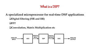
  • 1. What is a DSP? A specialized microprocessor for real-time DSP applications Digital filtering (FIR and IIR) FFT Convolution, Matrix Multiplication etc ADC DAC DSP ANALOG INPUT ANALOG OUTPUT DIGITAL INPUT DIGITAL OUTPUT
  • 2. Hardware used in DSP ASIC FPGA GPP DSP Performance Very High High Medium Medium High Flexibility Very low High High High Power consumption Very low low Medium Low Medium Development Time Long Medium Short Short
  • 3. Common DSP features • Harvard architecture • Dedicated single-cycle Multiply-Accumulate (MAC) instruction (hardware MAC units) • Single-Instruction Multiple Data (SIMD) Very Large Instruction Word (VLIW) architecture • Pipelining • Saturation arithmetic • Zero overhead looping • Hardware circular addressing • Cache • DMA
  • 4.
  • 5. INTRODUCTION In a normal computer that follows von Neumann architecture, instructions and data both are stored in same memory. So same buses are used to fetch instructions and data. This means CPU cannot do both things together (read a instruction and read/write data). Harvard Architecture is the computer architecture that contains separate storage and separate buses (signal path) for instruction and data. It was basically developed to overcome the bottleneck of Von Neumann Architecture. The main advantage of having separate buses for instruction and data is that CPU can access instructions and read/write data at the same time.
  • 6. Harvard Architecture Physically separate memories and paths for instruction and data DATA MEMORY PROGRAM MEMORY CPU
  • 7. STRUCTURE OF HARVARD ARCHITECTURE
  • 8. BUSES  Buses are used as signal pathways. In Harvard architecture there are separate buses for both instruction and data. Types of Buses:  Data Bus: It carries data among the main memory system, processor and I/O devices.  Data Address Bus: It carries the address of data from processor to main memory system.  Instruction Bus: It carries instructions among the main memory system, processor and I/O devices.  Instruction Address Bus: It carries the address of instructions from processor to main memory system.
  • 9. Operational registers There are different types of registers involved in it which are used for storing address of different types of instructions. For example, Memory Address Register and Memory Data Register are operational registers. ProgramCounter It has the location of the next instruction to be executed. Program counter then passes this next address to memory address register.
  • 10. Arithmetic and Logic Unit Arithmetic logic unit is that part of the CPU that operates all the calculations needed. It performs addition, subtraction, comparison, logical Operations, bit Shifting Operations and various arithmetic operations. Control unit Control unit the part of CPU that operates all processor control signals. It controls the input and output devices and also control the movement of instructions and data within the system.
  • 11. Input/output system  Input devices are used to read data into main memory with the help of CPU input instruction.  The information from a computer as output are given through Output devices.  Computer gives the results of computation with the help of output devices.
  • 12. ADVANTAGES  Since data and instructions are stored in separate buses there are very few chances of corruption.  Data that uses Read-Only mode and instructions which uses Read-Write mode are operated in the same way. They can also be accessed similarly.  Generally, two memories would be present, one for data and the other one for instructions, they have different cell sizes making use of the resources very effectively.  The bandwidth that is used for memory is more predictable.  They generally offer high performance as data and buses are kept in separate memory and travel on different buses.  Parallel access to data and instructions can be maintained.  Scheduling would no longer be required as there are separate buses for data and instructions.  Programmers can design the memory unit according to their requirements.  Control unit gets data and instructions from one memory. Thus, it simplifies the architecture of the control unit.
  • 13. disadvantages  The un-occupied data memory cannot be used by instructions and the free instruction memory cannot be used by data. Memory dedicated to each unit has to be balanced carefully.  The program cannot be written by the machine on its own as in Von Neumann Architecture.  Control Unit takes more time to develop and is on the expensive side.  There are 2 buses on the architecture. Which in the way means that the motherboard would be more complex, which in turn means that there would be two RAMs and thus tends to have a very complex cache design. That is the reason for it being used mostly inside the CPU and not outside of it.  Production of computer with 2 buses takes more time to get manufactured and is again on the expensive side like the control unit.  It has more pins on its IC’s. Therefore, it is very difficult to implement it.  It is not used widely, so the development of it would be on the backward edge.  It does not make most of the Central Processing Unit, always.
  • 14. Facts about Harvard architecture  Harvard Architecture speeds up the processor rate. Since data and instructions are stored in separate buses, it is very advantageous to many users.  Harvard Architecture follows the “Pipeline” arrangement. If the execution of one instruction is going on, the other instruction would be fetched from memory. This allows overlapping of instructions thus the execution rate is increased considerably.  RISC (Reduced Instruction Set Computer) and CISC (Complex Instruction Set Computer) are the methodologies used in Harvard Architecture. In RISC microcontroller data is 8 bits, whereas instructions are 12 bits or 16 bits wide. Thus, everything is executed at a time resulting in increased performance.  In CISC both data and instructions are 8 bits wide. They have generally over 200 instructions. But they cannot be executed at a time rather fetched simultaneously.  The execution unit consists of 2 Arithmetic and Logic Units, 1 shifter, 1 multiplier, accumulators, etc. Thus, they can execute arithmetic operations in a stable way and with excellent parallelism.  Many microcontrollers also use Lookup Table. (LUT). They made used for modulation purposes.
  • 15. Common DSP features Harvard architecture Dedicated single-cycle Multiply-Accumulate (MAC) instruction (hardware MAC units) Single-Instruction Multiple Data (SIMD) Very Large Instruction Word (VLIW) architecture Pipelining Saturation arithmetic Zero overhead looping Hardware circular addressing Cache DMA
  • 16. Single-Cycle MAC unit Multiplier Adder Register a x i i a x i i a x i-1 i-1 a x i i a x i-1 i-1 + Σ(a x ) i i i=0 n Can compute a sum of n-products in n cycles
  • 17. Single Instruction - Multiple Data (SIMD) A technique for data-level parallelism by employing a number of processing elements working in parallel
  • 18. Very Long Instruction Word (VLIW) A technique for instruction-level parallelism by executing instructions without dependencies (known at compile-time) in parallel Example of a single VLIW instruction: F=a+b; c=e/g; d=x&y; w=z*h; VLIW instruction F=a+b c=e/g d=x&y w=z*h PU PU PU PU a b F c d w e g x y z h
  • 20. Pipelining DSPs commonly feature deep pipelines TMS320C6x processors have 3 pipeline stages with a number of phases (cycles): Fetch Program Address Generate (PG) Program Address Send (PS) Program ready wait (PW) Program receive (PR) Decode Dispatch (DP) Decode (DC) Execute 6 to 10 phases
  • 21. Saturation Arithmetic Fixed range for operations like addition and multiplication Normal overflow and underflow produce the maximum and minimum allowed value, respectively Associativity and distributivity no longer apply 1 signed byte saturation arithmetic examples: 64 + 69 = 127 -127 – 5 = -128 (64 + 70) – 25 = 122 ≠ 64 + (70 -25) = 109
  • 22. ZeroOverheadLooping Hardware support for loops with a constant number of iterations using hardware loop counters and loop buffers No branching No loop overhead No pipeline stalls or branch prediction No need for loop unrolling
  • 23. Hardware CircularAddressing A data structure implementing a fixed length queue of fixed size objects where objects are added to the head of the queue while items are removed from the tail of the queue. Requires at least 2 pointers (head and tail) Extensively used in digital filtering y[n] = a0x[n]+a1x[n-1]+…+akx[n-k] X[n] X[n-1] X[n-2] X[n-3] X[n] X[n-1] X[n-2] X[n-3] Head Tail Cycle1 Cycle2
  • 24. Direct Memory Access (DMA) The feature that allows peripherals to access main memory without the intervention of the CPU Typically, the CPU initiates DMA transfer, does other operations while the transfer is in progress, and receives an interrupt from the DMA controller once the operation is complete. Can create cache coherency problems (the data in the cache may be different from the data in the external memory after DMA)
  • 25. Cache memory Separate instruction and data L1 caches (Harvard architecture) Cache coherence protocols required, since most systems use DMA
  • 26. DSP vs. Microcontroller DSP Harvard Architecture VLIW/SIMD (parallel execution units) No bit level operations Hardware MACs DSP applications Microcontroller Mostly von Neumann Architecture Single execution unit Flexible bit-level operations No hardware MACs Control applications
  • 30. Multiplier and Accumulator Unit(MAC) MAC is composed of an adder, multiplier and an accumulator. Usually adders implemented are Carry- Select or Carry-Save adders, as speed is of utmost importance in DSP. One implementation of the multiplier could be as a parallel array multiplier. The inputs for the MAC are to be fetched from memory location and fed to the multiplier block of the MAC, which will perform multiplication and give the result to adder which will accumulate the result and then will store the result into a memory location. This entire process is to be achieved in a single clock cycle
  • 31. Multiplier and Accumulator Unit(MAC) The architecture of the MAC unit consists of one 16 bit register, one 16-bit Modified Booth Multiplier, 32-bit accumulator. To multiply the values of A and B, Modified Booth multiplier is used instead of conventional multiplier because Modified Booth multiplier can increase the MAC unit design speed and reduce multiplication complexity. SPST Adder is used for the addition of partial products and a register is used for accumulation. The product of Ai X Bi is always fed back into the 32-bit accumulator and then added again with the next product Ai x Bi. This MAC unit is capable of multiplying and adding with previous product consecutively up to as many as times.
  • 33. Design of MAC In most of the digital signal processing (DSP) applications the critical operations usually involve many multiplications and/or accumulations. For real-time signal processing, a high speed and high throughput Multiplier-Accumulator (MAC) is always a key to achieve a high performance digital signal processing system. In the last few years, the main consideration of MAC design is to enhance its speed. This is because; speed and throughput rate is always the concern of digital signal processing system. But for the epoch of personal communication Low power design also becomes another main design consideration. This is because; battery energy available for these portable products limits the power consumption of the system
  • 34. Design of MAC Therefore, the various Pipelined multiplier/accumulator architectures and circuit design techniques which are suitable for implementing high throughput signal processing algorithms and at the same time achieve low power consumption. A conventional MAC unit consists of (fast multiplier) multiplier and an accumulator that contains the sum of the previous consecutive products The main goal of a DSP processor design is to enhance the speed of the MAC unit, and at the same time limit the power consumption. In a pipelined MAC circuit, the delay of pipeline stage is the delay of a 1-bit full adder. Estimating this delay will assist in identifying the overall delay of the pipelined MAC.
  • 35. Hardware architecture of the EnhancedMAC
  • 36. Hardware architecture of the EnhancedMAC If an operation to multiply two –bit numbers and accumulates into a 2-bit number is considered, the critical path is determined by the 2-bit accumulation operation. If a pipeline scheme is applied for each step in the standard design, the delay of the last accumulator must be reduced in order to improve the performance of the MAC.  The overall performance of the proposed MAC is improved by eliminating the accumulator itself by combining it with the CSA function. If the accumulator has been eliminated, the critical path is then determined by the final adder in the multiplier. The basic method to improve the performance of the final adder is to decrease the number of input bits. In order to reduce this number of input bits
  • 37. Hardware architecture of the EnhancedMAC The multiple partial products are compressed into a sum and a carry by CSA. The number of bits of sums and carries to be transferred to the final adder is reduced by adding the lower bits of sums and carries in advance within the range in which the overall performance will not be degraded. A 2-bit CLA is used to add the lower bits in the CSA. In addition, to increase the output rate when pipelining is applied, the sums and carrys from the CSA are accumulated instead of the outputs from the final adder in the manner that the sum and carry from the CSA in the previous cycle are inputted to CSA. Due to this feedback of both sum and carry, the number of inputs to CSA increases, compared to the standard design and . In order to efficiently solve the increase in the amount of data, a CSA architecture is modified to treat the sign bit.
  • 38. ADDRESSING MODES OF TMS320C54X Direct addressing Memory-mapped register addressing Indirect addressing Immediate addressing Dedicated-register addressing Circular addressing
  • 39. DIRECT Addressing Mode In Direct addressing mode the lower 7 bits of the data memory address are specified in the instruction itself. The 16 bit data memory address is formed by using either 9 bits of Data Pointer in status register-0 and the 16 bit of Stack Pointer When DP is used, the 9 bits of the DP is the upper 9 bits of the 16 bit address and the lower 7 bits are the address directly specified by the instruction When SP is used, the 16 bit content of SP is added to 7 bits specified in the instruction to form 16 bit address.
  • 40. MEMORY MAPPED REGISTER Addressing In memory-mapped register addressing, the address of the memory-mapped register can be specified as direct address in the instruction. The memory-mapped register addressing is a special case of direct addressing in which only page offset address is used to access the memory and the default page address is 000h. Therefore, the data pointer need not be loaded with page address for this addressing mode.
  • 41. INDIRECTAddressing Mode In indirect addressing mode, the data memory address is specified by the content of one of the eight auxiliary registers, AR0 - AR7. The AR ( Auxiliary Register) currently used for accessing data is denoted by ARP (Auxiliary Register Pointer). In indirect addressing mode, the content of AR can be updated automatically either after or before the operand is fetched. The syntax used in the operand field of instruction for modifying the content AR are
  • 42. Immediate Addressing Mode In immediate Addressing, the data is specified as a part of the Instruction . In this addressing the instruction will carry a 3-bit/5- bit/8-bit/9-bit/16-bit constant, which is the data to be operated by the instruction. The Immediate Constant is specified with the # Symbol
  • 43. BIT REVERSEDAddressing Mode In bit reversed addressing, the data memory address is specified by AR like indirect addressing, but the content of AR is incremented/decremented in order to generate the data memory address in the bit reversed order, using the content of index register. (The bit reversed addressing is a special case of indirect addressing).
  • 44. DEDICATEDAddressing Mode • In dedicated register addressing mode, the address of one of the operands is specified by a dedicated CPU register BMAR (Block Move Address Register). In this addressing mode, the address of the memory block to be accessed can be changed during execution of the program. • In another case of dedicated register addressing, one of the operands is the content of a dedicated CPU register DBMR (Dynamic Bit Manipulation Register).
  • 45. CIRCULARAddressing Mode • The circular addressing is similar to indirect addressing. This addressing mode allows the specified memory buffer to be accessed sequentially with a pointer that automatically wraps around to the beginning of the buffer when the last location is accessed. • In circular addressing mode, when the address pointer is incremented, the address in AR will be checked with the end address of the circular buffer, and if it exceeds the end address then the address is made equal to start address of the circular buffer. • In order to hold the start and end addresses of the circular buffer, the TMS320C5x has four circular buffer registers, namely, • CBSR1 : Circular Buffer-1 Start address Register • CBSR2 : Circular Buffer-2 Start address Register • CBER1 : Circular Buffer-1 End address Register • CBER2 : Circular Buffer-2 End address Register • With the help of the above registers, at any one time, two circular buffers can be defined. A Circular Buffer Control Register (CBCR) is used to enable/disable the circular buffers.
  • 46. WHAT IS PIPELINING???  In processors without pipelining, the execution of instruction is performed one by one, i.e., after complete execution of an instruction the next instruction is fetched from memory.  In processors with pipelining, the instruction execution is divided into various phases/stages and execution of different phases of two or more instructions are performed in parallel.  The number of instructions that can be executed in parallel is called depth or level of pipelining.
  • 47. PHASES  Fetch (F) — This phase fetches the instruction words from memory and updates the program counter (PC).  Decode (D) — This phase decodes the instruction word and performs address generation and ARAU(auxiliary register arithmetic unit) updates of auxiliary registers.  Read (R) — This phase reads operands from memory, if required. If the instruction uses indirect addressing mode, it will read the memory location pointed at by the ARP before the update of the previous decode phase  Execute (E) — This phase performs any specify operation, and, if required, writes results of a previous operation to memory Let us consider a processor in which the instruction execution is divided into the following four phases.
  • 48. Let Inst1, Inst2, Inst3, ..... be the instructions to be executed sequentially. The execution of the four phases of the instructions for subsequent clock cycles are listed in table . In this pipelining when the phase 4 of 1st instruction is executed, the phase 3 of 2nd instruction, the phase 2 of 3rd instruction and the phase 1 of 4th instruction are also executed simultaneously. Table: Pipelining of Instruction Execution
  • 49. Types of pipeline It is divided into 2 categories: 1. Arithmetic Pipeline 2. Instruction Pipeline Arithmetic Pipeline: Arithmetic pipelines are usually found in most of the computers. They are used for floating point operations, multiplication of fixed point numbers etc. For example: The input to the Floating Point Adder pipeline is: X = A*2^a Y = B*2^b Here A and B are mantissas (significant digit of floating point numbers), while a and b are exponents. The floating point addition and subtraction is done in 4 parts: 1. Compare the exponents. 2. Align the mantissas. 3. Add or subtract mantissas 4. Produce the result. Registers are used for storing the intermediate results between the above operations.
  • 50. Instruction Pipeline Instruction Pipeline In this a stream of instructions can be executed by overlapping fetch, decode and execute phases of an instruction cycle. This type of technique is used to increase the throughput of the computer system. An instruction pipeline reads instruction from the memory while previous instructions are being executed in other segments of the pipeline. Thus we can execute multiple instructions simultaneously. The pipeline will be more efficient if the instruction cycle is divided into segments of equal duration. Pipeline Conflicts There are some factors that cause the pipeline to deviate its normal performance. Some of these factors are given below: 1. Timing Variations :All stages cannot take same amount of time. This problem generally occurs in instruction processing where different instructions have different operand requirements and thus different processing time 2. Data Hazards: When several instructions are in partial execution, and if they reference same data then the problem arises. We must ensure that next instruction does not attempt to access data before the current instruction, because this will lead to incorrect results. 3. Branching: In order to fetch and execute the next instruction, we must know what that instruction is. If the present instruction is a conditional branch, and its result will lead us to the next instruction, then the next instruction may not be known until the current one is processed. 4. Interrupts :Interrupts set unwanted instruction into the instruction stream. Interrupts effect the execution of instruction.
  • 51. Advantages of Pipelining: • The cycle time of the processor is reduced. • It increases the throughput of the system. • It makes the system reliable Disadvantages of Pipelining: • The design of pipelined processor is complex and costly to manufacture. • The instruction latency is more.
  • 53. Instructions of TMS320C5x Processors The TMS320C5x processors instruction set consists of instructions that supports both numeric-intensive signal processing operations and general-purpose applications. The instructions can be classified into following groups. 1. Arithmetic instructions 2. Logical instructions 3. Branch/control instructions 4. Load/store instructions 5. Block move instructions
  • 54. ARITHMETIC INSTRUCTIONS  Add instructions  Subtract instructions  Multiply instructions  Multiply-accumulate instructions  Multiply-subtract instructions  Double (32-bit operand) instructions  Application-specific instructions
  • 55. Logical INSTRUCTIONS  AND instructions  OR instructions  XOR instructions  Shift instructions  Test instructions
  • 56. Branch/control instructions  Branch instructions  Call instructions  Interrupt instructions  Return instructions  Repeat instructions  Stack-manipulating instructions  Miscellaneous program-control instructions
  • 57. LOAD/STORE instructions  Load instructions  Store instructions  Conditional store instructions  Parallel load and store instructions  Parallel load and multiply instructions  Parallel store and add/subtract instructions  Parallel store and multiply instructions  Miscellaneous load-type and store-type instructions
  • 61.
  • 63.
  • 65.
  • 66.
  • 67.
  • 71.
  • 73. Symbols and Acronyms Used in the Instruction Set Summary
  • 74. Conditions for Branch, Call and Return Instructions