
Empfohlen
Empfohlen
Weitere ähnliche Inhalte
Was ist angesagt?
Was ist angesagt? (20)
Ähnlich wie 10Gb/s DWDM XFP Transceiver Hot Pluggable, Duplex LC, +3.3V & +5V, 100GHz ITU Grid C Band, EML/APD Single mode, 80km, 0~70°C
Ähnlich wie 10Gb/s DWDM XFP Transceiver Hot Pluggable, Duplex LC, +3.3V & +5V, 100GHz ITU Grid C Band, EML/APD Single mode, 80km, 0~70°C (20)
Kürzlich hochgeladen
Kürzlich hochgeladen (20)
10Gb/s DWDM XFP Transceiver Hot Pluggable, Duplex LC, +3.3V & +5V, 100GHz ITU Grid C Band, EML/APD Single mode, 80km, 0~70°C
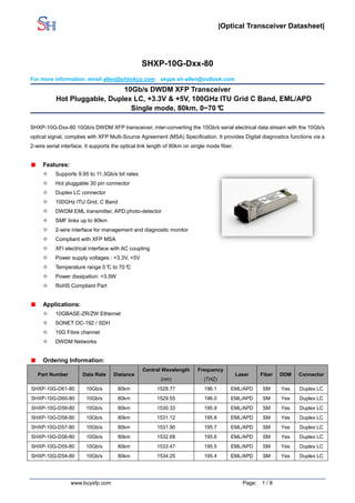
- 1. |Optical Transceiver Datasheet| www.buysfp.com Page: 1 / 8 SHXP-10G-Dxx-80 For more information: email allen@shlinkco.com skype sh-allen@outlook.com 10Gb/s DWDM XFP Transceiver Hot Pluggable, Duplex LC, +3.3V & +5V, 100GHz ITU Grid C Band, EML/APD Single mode, 80km, 0~70°C SHXP-10G-Dxx-80 10Gb/s DWDM XFP transceiver, inter-converting the 10Gb/s serial electrical data stream with the 10Gb/s optical signal, complies with XFP Multi-Source Agreement (MSA) Specification. It provides Digital diagnostics functions via a 2-wire serial interface. It supports the optical link length of 80km on single mode fiber. Features: Supports 9.95 to 11.3Gb/s bit rates Hot pluggable 30 pin connector Duplex LC connector 100GHz ITU Grid, C Band DWDM EML transmitter, APD photo-detector SMF links up to 80km 2-wire interface for management and diagnostic monitor Compliant with XFP MSA XFI electrical interface with AC coupling Power supply voltages : +3.3V, +5V Temperature range 0°C to 70°C Power dissipation: <3.5W RoHS Compliant Part Applications: 10GBASE-ZR/ZW Ethernet SONET OC-192 / SDH 10G Fibre channel DWDM Networks Ordering Information: Part Number Data Rate Distance Central Wavelength (nm) Frequency (THZ) Laser Fiber DDM Connector SHXP-10G-D61-80 10Gb/s 80km 1528.77 196.1 EML/APD SM Yes Duplex LC SHXP-10G-D60-80 10Gb/s 80km 1529.55 196.0 EML/APD SM Yes Duplex LC SHXP-10G-D59-80 10Gb/s 80km 1530.33 195.9 EML/APD SM Yes Duplex LC SHXP-10G-D58-80 10Gb/s 80km 1531.12 195.8 EML/APD SM Yes Duplex LC SHXP-10G-D57-80 10Gb/s 80km 1531.90 195.7 EML/APD SM Yes Duplex LC SHXP-10G-D56-80 10Gb/s 80km 1532.68 195.6 EML/APD SM Yes Duplex LC SHXP-10G-D55-80 10Gb/s 80km 1533.47 195.5 EML/APD SM Yes Duplex LC SHXP-10G-D54-80 10Gb/s 80km 1534.25 195.4 EML/APD SM Yes Duplex LC
- 2. |Optical Transceiver Datasheet| www.buysfp.com Page: 2 / 8 SHXP-10G-D53-80 10Gb/s 80km 1535.04 195.3 EML/APD SM Yes Duplex LC SHXP-10G-D52-80 10Gb/s 80km 1535.82 195.2 EML/APD SM Yes Duplex LC SHXP-10G-D51-80 10Gb/s 80km 1536.61 195.1 EML/APD SM Yes Duplex LC SHXP-10G-D50-80 10Gb/s 80km 1537.40 195.0 EML/APD SM Yes Duplex LC SHXP-10G-D49-80 10Gb/s 80km 1538.19 194.9 EML/APD SM Yes Duplex LC SHXP-10G-D48-80 10Gb/s 80km 1538.98 194.8 EML/APD SM Yes Duplex LC SHXP-10G-D47-80 10Gb/s 80km 1539.77 194.7 EML/APD SM Yes Duplex LC SHXP-10G-D46-80 10Gb/s 80km 1540.56 194.6 EML/APD SM Yes Duplex LC SHXP-10G-D45-80 10Gb/s 80km 1541.35 194.5 EML/APD SM Yes Duplex LC SHXP-10G-D44-80 10Gb/s 80km 1542.14 194.4 EML/APD SM Yes Duplex LC SHXP-10G-D43-80 10Gb/s 80km 1542.94 194.3 EML/APD SM Yes Duplex LC SHXP-10G-D42-80 10Gb/s 80km 1543.73 194.2 EML/APD SM Yes Duplex LC SHXP-10G-D41-80 10Gb/s 80km 1544.53 194.1 EML/APD SM Yes Duplex LC SHXP-10G-D40-80 10Gb/s 80km 1545.32 194.0 EML/APD SM Yes Duplex LC SHXP-10G-D39-80 10Gb/s 80km 1546.12 193.9 EML/APD SM Yes Duplex LC SHXP-10G-D38-80 10Gb/s 80km 1546.92 193.8 EML/APD SM Yes Duplex LC SHXP-10G-D37-80 10Gb/s 80km 1547.72 193.7 EML/APD SM Yes Duplex LC SHXP-10G-D36-80 10Gb/s 80km 1548.51 193.6 EML/APD SM Yes Duplex LC SHXP-10G-D35-80 10Gb/s 80km 1549.32 193.5 EML/APD SM Yes Duplex LC SHXP-10G-D34-80 10Gb/s 80km 1550.12 193.4 EML/APD SM Yes Duplex LC SHXP-10G-D33-80 10Gb/s 80km 1550.92 193.3 EML/APD SM Yes Duplex LC SHXP-10G-D32-80 10Gb/s 80km 1551.72 193.2 EML/APD SM Yes Duplex LC SHXP-10G-D31-80 10Gb/s 80km 1552.52 193.1 EML/APD SM Yes Duplex LC SHXP-10G-D30-80 10Gb/s 80km 1553.33 193.0 EML/APD SM Yes Duplex LC SHXP-10G-D29-80 10Gb/s 80km 1554.13 192.9 EML/APD SM Yes Duplex LC SHXP-10G-D28-80 10Gb/s 80km 1554.94 192.8 EML/APD SM Yes Duplex LC SHXP-10G-D27-80 10Gb/s 80km 1555.75 192.7 EML/APD SM Yes Duplex LC SHXP-10G-D26-80 10Gb/s 80km 1556.55 192.6 EML/APD SM Yes Duplex LC SHXP-10G-D25-80 10Gb/s 80km 1557.36 192.5 EML/APD SM Yes Duplex LC SHXP-10G-D24-80 10Gb/s 80km 1558.17 192.4 EML/APD SM Yes Duplex LC SHXP-10G-D23-80 10Gb/s 80km 1558.98 192.3 EML/APD SM Yes Duplex LC SHXP-10G-D22-80 10Gb/s 80km 1559.79 192.2 EML/APD SM Yes Duplex LC SHXP-10G-D21-80 10Gb/s 80km 1560.61 192.1 EML/APD SM Yes Duplex LC SHXP-10G-D20-80 10Gb/s 80km 1561.42 192.0 EML/APD SM Yes Duplex LC SHXP-10G-D19-80 10Gb/s 80km 1562.23 191.9 EML/APD SM Yes Duplex LC SHXP-10G-D18-80 10Gb/s 80km 1563.05 191.8 EML/APD SM Yes Duplex LC SHXP-10G-D17-80 10Gb/s 80km 1563.86 191.7 EML/APD SM Yes Duplex LC
- 3. |Optical Transceiver Datasheet| www.buysfp.com Page: 3 / 8 Absolute Maximum Ratings Parameter Symbol Min Max Unit Storage Temperature TST -40 +85 ℃ Case Operating Temperature TIP 0 +70 ℃ Supply Voltage 1 VCC3 -0.5 +4.0 V Supply Voltage 2 VCC5 -0.5 +6.0 V Electrical Characteristics (TOP = 0 to 70 °C) Parameter Symbol Min Typ Max Unit Note Supply Voltage 1 Vcc5 4.75 5.25 V Supply Voltage 2 Vcc3 3.13 3.45 V Supply Current – Vcc5 supply Icc5 250 mA Supply Current – Vcc3 supply Icc3 500 mA Module total power P 3.5 W Transmitter Input differential impedance Rin 100 Ω 1 Differential data input swing Vin,pp 150 820 mV Transmit Disable Voltage VD 2.0 Vcc V Transmit Enable Voltage VEN GND GND+ 0.8 V Transmit Disable Assert Time T_off 100 ms Tx Enable Assert Time T_on 100 ms Receiver Differential data output swing Vout,pp 300 500 850 mV Data output rise time tr 35 ps 2 Data output fall time tf 35 ps 2 LOS Fault VLOS fault Vcc – 0.5 VccHOST V 3 LOS Normal VLOS norm GND GND+0.5 V 3 Power Supply Rejection PSR See Note 4 below 4 Notes: 1. After internal AC coupling. 2. 20 – 80 % 3.Loss of Signal is open collector to be pulled up with a 4.7k – 10kohm resistor to 3.15 – 3.6V. Logic 0 indicates normal operation; logic 1 indicates no signal detected. 4. Per Section 2.7.1. in the XFP MSA Specification. Optical Parameters (TOP = 0 to 70°C) Parameter Symbol Min Typ Max Unit Ref. Transmitter Operating Date Rate BR 9.95 11.3 Gb/s Bit Error Rate BER 10 -12 Maximum Launch Power PMAX 0 +5 dBm 1 Optical Wavelength-End Of Life λ X-100 X X+100 pm Optical Wavelength-Beginning Of Life λ X-25 X X+25 pm Optical Extinction Ratio ER 8.2 dB Spectral Width@-20dB Δλ 1 nm
- 4. |Optical Transceiver Datasheet| www.buysfp.com Page: 4 / 8 Sidemode Supression ratio SSRmin 30 dB Rise/Fall Time (20%~80%) Tr/Tf 35 ps Average Launch power of OFF Transmitter POFF -30 dBm Tx Jitter Txj Compliant with each standard requirements Optical Eye Mask IEEE802.3ae 2 Receiver Operating Date Rate BR 9.95 11.3 Gb/s Receiver Sensitivity Sen -23 dBm 2 Maximum Input Power PMAX -7 dBm 2 Optical Center Wavelength λC 1260 1600 nm Receiver Reflectance Rrx -27 dB LOS De-Assert LOSD -24 dBm LOS Assert LOSA -34 dBm LOS Hysteresis LOSH 0.5 5 dB Notes: 1. The optical power is launched into SMF. 2. Measured with a PRBS 231-1 test pattern @10.3125Gbps BER<10-12. Pin Assignment Diagram of Host Board Connector Block Pin Numbers and Name
- 5. |Optical Transceiver Datasheet| www.buysfp.com Page: 5 / 8 Pin Function Definitions Pin Logic Symbol Name/Description Note 1 GND Module Ground 1 2 VEE5 Optional –5.2 Power Supply – Not required 3 LVTTL-I Mod-Desel Module De-select; When held low allows the module to respond to 2-wire serial interface commands 4 LVTTL-O Interrupt Interrupt (bar); Indicates presence of an important condition which can be read over the serial 2-wire interface 2 5 LVTTL-I TX_DIS Transmitter Disable; Transmitter laser source turned off 6 VCC5 +5 Power Supply 7 GND Module Ground 1 8 VCC3 +3.3V Power Supply 9 VCC3 +3.3V Power Supply 10 LVTTL-I SCL Serial 2-wire interface clock 2 11 LVTTL- I/O SDA Serial 2-wire interface data line 2 12 LVTTL-O Mod_Abs Module Absent; Indicates module is not present. Grounded in the module. 2 13 LVTTL-O Mod_NR Module Not Ready; 2 14 LVTTL-O RX_LOS Receiver Loss of Signal indicator 2 15 GND Module Ground 1 16 GND Module Ground 1 17 CML-O RD- Receiver inverted data output 18 CML-O RD+ Receiver non-inverted data output 19 GND Module Ground 1 20 VCC2 +1.8V Power Supply – Not required 21 LVTTL-I P_Down/RST Power Down; When high, places the module in the low power stand-by mode and on the falling edge of P_Down initiates a module reset Reset; The falling edge initiates a complete reset of the module including the 2-wire serial interface, equivalent to a power cycle. 22 VCC2 +1.8V Power Supply – Not required 23 GND Module Ground 1 24 PECL-I RefCLK+ Reference Clock non-inverted input, AC coupled on the host board – Not required 3 25 PECL-I RefCLK- Reference Clock inverted input, AC coupled on the host board – Not required 3 26 GND Module Ground 1 27 GND Module Ground 1 28 CML-I TD- Transmitter inverted data input 29 CML-I TD+ Transmitter non-inverted data input 30 GND Module Ground 1 Note: 1. Module circuit ground is isolated from module chassis ground within the module. 2. Open collector; should be pulled up with 4.7k – 10k ohms on host board to a voltage between 3.15Vand 3.45V. 3. A Reference Clock input is not required.
- 6. |Optical Transceiver Datasheet| www.buysfp.com Page: 6 / 8 Digital Diagnostic Functions As defined by the XFP MSA 1, SH’s XFP transceivers provide digital diagnostic functions via a 2-wire serial interface, which allows real-time access to the following operating parameters: Transceiver temperature Laser bias current Transmitted optical power Received optical power Transceiver supply voltage It also provides a sophisticated system of alarm and warning flags, which may be used to alert end-users when particular operating parameters are outside of a factory-set normal range. The operating and diagnostics information is monitored and reported by a Digital Diagnostics Transceiver Controller (DDTC) inside the transceiver, which is accessed through the 2-wire serial interface. When the serial protocol is activated, the serial clock signal (SCL pin) is generated by the host. The positive edge clocks data into the XFP transceiver into those segments of its memory map that are not write-protected. The negative edge clocks data from the XFP transceiver. The serial data signal (SDA pin) is bi-directional for serial data transfer. The host uses SDA in conjunction with SCL to mark the start and end of serial protocol activation. The memories are organized as a series of 8-bit data words that can be addressed individually or sequentially. The 2-wire serial interface provides sequential or random access to the 8 bit parameters, addressed from 000h to the maximum address of the memory. For more detailed information including memory map definitions, please see the XFP MSA Specification.
- 7. |Optical Transceiver Datasheet| www.buysfp.com Page: 7 / 8 Recommended Circuit Recommended Host Board Power Supply Circuit Recommended High-speed Interface Circuit
- 8. |Optical Transceiver Datasheet| www.buysfp.com Page: 8 / 8 Mechanical Dimensions