
Empfohlen
Empfohlen
Weitere ähnliche Inhalte
Was ist angesagt?
Was ist angesagt? (20)
Ähnlich wie Micro and nano manufacturing
Ähnlich wie Micro and nano manufacturing (20)
Kürzlich hochgeladen
Kürzlich hochgeladen (20)
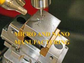
Micro and nano manufacturing
- 2. “Micro manufacturing is the set of processes or techniques used to fabricate micro components or to create a micro features on macro/micro parts”. Micro - (symbol μ)Confirmed in 1960, the terms comes from the Greek μικρός (mikrós), meaning "small". There are various types of micro manufacturing process such as subtractive, additive, mass containing, joining. These process are sub divided into various process like, Diamond turning, laser welding, micro drilling, micro casting, micro molding.
- 3. Diamond turning is mechanical machining of precision element using laths or derivative machine tool equipped with natural or synthetic diamond tipped tool bit. Diamond turning has been used to machine microgrooves 2.5-μm wide by 1.6-μm deep in copper with 10 mm surface finishing. Optical elements produce by the means of diamond turning are used in optical assemblies in telescope, video projector, missile guidance system, lasers etc.
- 4. There are tow types of laser beam welding such as surface heating, TTIR welding. Through transmission infrared (TTIR) welding: It is based on the concept of passing laser radiations through one of the component to be welded while having the second component absorb the light at the interface. This absorption results in heating and melting of the interface and allows the part to be welded.
- 6. Manufacturing at nano scale is known as Nano manufacturing. One nanometer is one billionth of a meter i.e. 10−9 The term Nano was first proposed by K . Eric Drexler in the 1970s. There are two basic approaches to nano manufacturing either “top-down” or “bottom-up” Top down approaches is further divided in Focusd beam lithography and nano imprint lithography Bottom down approach is divided into CVD and Dip pen lithography.
- 7. As the diagram shows, the gallium (Ga+) primary ion beam hits the sample surface and sputters a small amount of material, which leaves the surface as either secondary ions (i+ or i-) or neutral atoms (n0). The primary beam also produces secondary electrons (e−). As the primary beam rosters on the sample surface, the signal from the sputtered ions or secondary electrons is collected to form an image.
- 8. Nano imprint lithography is a lithography technique we use to make nanostructure substrates The stamps are pressed into polymeric material (resist) that was previously deposited on the substrate. When the stamp is filled with polymer, it is treated by UV light through the stamp, obtaining the stamp shape. A residual layer of resist is left and can be removed A metal layer can be deposited on the sample, when the resist is removed, the nanoscale metal structure is left on the substrate.
- 9. Chemical vapor deposition (CVD) is a chemical process used to produce high quality, high- performance, solid materials. The process is often used in the semiconductor industry to produce thin films. In typical CVD, the wafer (substrate) is exposed to one or more volatile precursors, which react and/or decompose on the substrate surface to produce the desired deposit. Frequently, volatile by-products are also produced, which are removed by gas flow through the reaction chamber.
- 10. In DPN the tip of AFM cantilever as a “pen”, which is coated with chemical compound acting as an “ink” and put in contact with substrate, the “paper”. Note that “liquid ink” are governed by a very different deposition mechanism when compared to “molecular ink”. Molecular ink diffusing from a nanoscale tip to a surface through a water ,meniscus.
- 12. Fig.1 shows an array of holes, each measuring approximately 125 nanometers in length, was precision-drilled with a computer-controlled focused ion beam. Fig.2 shows, a focused ion beam created this two- micron-wide gear, seen here at 50,000x magnification Fig.2
- 13. Micromanufacturing Engineering and Technology By Yi Qin. Micro and nano manufacturing By Mark J. Jackson. Micro fabrication and nano manufacturing By Mark J. Jackson. Images imported from Google images.