Cara Menggugurkan Sperma Yang Masuk Rahim Biyar Tidak Hamil
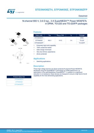
Original N-CHANNEL MOSFET P3NK90ZF STD3NK90Z STP3NK90Z STP3NK90ZFP 900V - 4.1ohm - 3A TO-220 New STMicroelectronics
1. DPAK
1
2
3
TAB
TO-220
1
2
3
TO-220FP
1
32
TAB
D(2, TAB)
G(1)
S(3) AM01475V1
Features
Order code VDS RDS(on) max. ID Package
STD3NK90ZT4
900 V 4.8 Ω 3 A
DPAK
STP3NK90Z TO-220
STP3NK90ZFP TO-220FP
• Extremely high dv/dt capability
• 100% avalanche tested
• Gate charge minimized
• Very low intrinsic capacitance
• Zener-protected
Applications
• Switching applications
Description
These high-voltage devices are Zener-protected N-channel Power MOSFETs
developed using the SuperMESH™ technology by STMicroelectronics, an
optimization of the well-established PowerMESH™. In addition to a significant
reduction in on-resistance, these devices are designed to ensure a high level of dv/dt
capability for the most demanding applications.
Product status link
STD3NK90ZT4
STP3NK90Z
STP3NK90ZFP
N-channel 900 V, 3.6 Ω typ., 3 A SuperMESH™ Power MOSFETs
in DPAK, TO-220 and TO-220FP packages
STD3NK90ZT4, STP3NK90Z, STP3NK90ZFP
Datasheet
DS2980 - Rev 3 - August 2018
For further information contact your local STMicroelectronics sales office.
www.st.com
2. 1 Electrical ratings
Table 1. Absolute maximum ratings
Symbol Parameter
Value
Unit
DPAK, TO-220 TO-220FP
VDS Drain-source voltage 900 V
VGS Gate-source voltage ± 30 V
ID Drain current (continuous) at TC = 25 °C 3 3 (1) A
ID Drain current (continuous) at TC = 100 °C 1.89 1.89 (1) A
IDM
(2)
Drain current (pulsed) 12 12 (1) A
PTOT Total dissipation at TC = 25 °C 90 25 W
ESD
Gate-source human body model
(R = 1,5 kΩ, C = 100 pF)
4 kV
dv/dt (3) Peak diode recovery voltage slope 4.5 V/ns
VISO
Insulation withstand voltage (RMS) from all three
leads to external heat sink (t = 1 s; Tc = 25 °C)
2.5 kV
Tj Operating junction temperature range
-55 to 150 °C
Tstg Storage temperature range
1. Limited by maximum junction temperature.
2. Pulse width limited by safe operating area.
3. ISD ≤ 3 A, di/dt ≤ 200 A/μs, VDS(peak) ≤ V(BR)DSS, VDD = 80% V(BR)DSS.
Table 2. Thermal data
Symbol Parameter
Value
Unit
DPAK TO-220 TO-220FP
Rthj-case Thermal resistance junction-case 1.38 5
°C/WRthj-amb Thermal resistance junction-ambient 62.5
Rthj-pcb
(1)
Thermal resistance junction-pcb 50
1. When mounted on 1inch² FR-4, 2 Oz copper board.
Table 3. Avalanche characteristics
Symbol Parameter Value Unit
IAR
(1)
Avalanche current, repetitive or not-repetitive 3 A
EAS
(2)
Single pulse avalanche energy 180 mJ
1. Pulse width limited by Tjmax.
2. Starting Tj = 25°C, ID = IAR, VDD = 50 V.
STD3NK90ZT4, STP3NK90Z, STP3NK90ZFP
Electrical ratings
DS2980 - Rev 3 page 2/24
3. 2 Electrical characteristics
(TCASE = 25 °C unless otherwise specified)
Table 4. On/off states
Symbol Parameter Test conditions Min. Typ. Max. Unit
V(BR)DSS
Drain-source breakdown
voltage
ID = 1 mA, VGS = 0 V 900 V
IDSS
Zero gate voltage drain
current
VGS = 0 V, VDS = 900 V 1 µA
VGS = 0 V, VDS = 900 V, TC = 125 °C (1)
50 μA
IGSS
Gate body leakage
current
VDS = 0 V, VGS = ±20 V ±10 μA
VGS(th) Gate threshold voltage VDS = VGS, ID = 50 µA 3 3.75 4.5 V
RDS(on)
Static drain-source on
resistance
VGS = 10 V, ID = 1.5 A 3.6 4.8 Ω
1. Defined by design, not subject to production test.
Table 5. Dynamic
Symbol Parameter Test conditions Min. Typ. Max. Unit
Ciss Input capacitance
VDS = 25 V, f = 1 MHz, VGS = 0 V -
590
- pF
Coss Output capacitance 63
Crss
Reverse transfer
capacitance
13
Coss eq.
(1) Equivalent output
capacitance
VDS = 0 to 720 V, VGS = 0 V - 35 - pF
Qg Total gate charge
VDD = 720 V, ID = 3 A, VGS = 0 to 10 V
(see Figure 16. Test circuit for gate charge
behavior)
-
22.7
- nCQgs Gate-source charge 4.2
Qgd Gate-drain charge 12
1. Coss eq. is defined as a constant equivalent capacitance giving the same charging time as Coss when VDS increases from 0
to 80% VDSS.
Table 6. Switching times
Symbol Parameter Test conditions Min. Typ. Max. Unit
td(on) Turn-on delay time VDD = 450 V, ID = 1.5 A,
RG = 4.7 Ω, VGS = 10 V
(see Figure 15. Test circuit for resistive load
switching times and Figure 20. Switching
time waveform)
-
18
- ns
tr Rise time 7
td(off) Turn-off delay time 45
tf Fall time 18
STD3NK90ZT4, STP3NK90Z, STP3NK90ZFP
Electrical characteristics
DS2980 - Rev 3 page 3/24
4. Table 7. Source drain diode
Symbol Parameter Test conditions Min. Typ. Max. Unit
ISD Source-drain current
-
3
A
ISDM
(1) Source-drain current
(pulsed)
12
VSD
(2)
Forward on voltage ISD = 3 A, VGS = 0 V - 1.6 V
trr Reverse recovery time ISD = 3 A, di/dt = 100 A/µs
VDD = 40 V, TJ = 150 °C
(see Figure 17. Test circuit for inductive
load switching and diode recovery times)
-
510 ns
Qrr Reverse recovery charge 2.2 μC
IRRM Reverse recovery current 8.7 A
1. Pulse width limited by safe operating area.
2. Pulsed: pulse duration = 300 μs, duty cycle 1.5%.
Table 8. Gate-source Zener diode
Symbol Parameter Test conditions Min. Typ. Max. Unit
V(BR)GSO
Gate-source breakdown
voltage
IGS = ±1 mA, ID = 0 A 30 - - V
The built-in back-to-back Zener diodes are specifically designed to enhance the ESD performance of the device.
The Zener voltage facilitates efficient and cost-effective device integrity protection, thus eliminating the need for
additional external componentry.
STD3NK90ZT4, STP3NK90Z, STP3NK90ZFP
Electrical characteristics
DS2980 - Rev 3 page 4/24
5. 2.1 Electrical characteristics curves
Figure 1. Safe operating area for DPAK, TO-220 Figure 2. Thermal impedance for DPAK, TO-220
Figure 3. Safe operating area for TO-220FP Figure 4. Thermal impedance for TO-220FP
δ=0.5
K
tp(s)10-4
10-3
10
-1
10
-2
δ=0.2
10-2
10
-3
10
0
10-1
Single pulse
0.05
0.02
0.01
0.1
GC20940_ZTH
Figure 5. Output characterisics Figure 6. Transfer characteristics
STD3NK90ZT4, STP3NK90Z, STP3NK90ZFP
Electrical characteristics curves
DS2980 - Rev 3 page 5/24
6. Figure 7. Static drain-source on resistance Figure 8. Gate charge vs gate-source voltage
Figure 9. Capacitance variations
Figure 10. Normalized gate threshold voltage vs
temperature
Figure 11. Normalized on resistance vs temperature Figure 12. Source-drain diode forward characteristics
STD3NK90ZT4, STP3NK90Z, STP3NK90ZFP
Electrical characteristics curves
DS2980 - Rev 3 page 6/24
7. Figure 13. Maximum avalanche energy vs temperature Figure 14. Normalized V(BR)DSS vs temperature
STD3NK90ZT4, STP3NK90Z, STP3NK90ZFP
Electrical characteristics curves
DS2980 - Rev 3 page 7/24
8. 3 Test circuits
Figure 15. Test circuit for resistive load switching times
AM01468v1
VD
RG
RL
D.U.T.
2200
μF VDD
3.3
μF+
pulse width
VGS
Figure 16. Test circuit for gate charge behavior
AM01469v1
47 kΩ
1 kΩ
47 kΩ
2.7 kΩ
1 kΩ
12 V
IG= CONST
100 Ω
100 nF
D.U.T.
+pulse width
VGS
2200
μF
VG
VDD
Figure 17. Test circuit for inductive load switching and
diode recovery times
AM01470v1
A
D
D.U.T.
S
B
G
25 Ω
A A
B
B
RG
G
D
S
100 µH
µF
3.3 1000
µF VDD
D.U.T.
+
_
+
fast
diode
Figure 18. Unclamped inductive load test circuit
AM01471v1
VD
ID
D.U.T.
L
VDD+
pulse width
Vi
3.3
µF
2200
µF
Figure 19. Unclamped inductive waveform
AM01472v1
V(BR)DSS
VDDVDD
VD
IDM
ID
Figure 20. Switching time waveform
AM01473v1
0
VGS 90%
VDS
90%
10%
90%
10%
10%
ton
td(on) tr
0
toff
td(off) tf
STD3NK90ZT4, STP3NK90Z, STP3NK90ZFP
Test circuits
DS2980 - Rev 3 page 8/24
9. 4 Package information
In order to meet environmental requirements, ST offers these devices in different grades of ECOPACK®
packages, depending on their level of environmental compliance. ECOPACK® specifications, grade definitions
and product status are available at: www.st.com. ECOPACK® is an ST trademark.
STD3NK90ZT4, STP3NK90Z, STP3NK90ZFP
Package information
DS2980 - Rev 3 page 9/24
10. 4.1 DPAK (TO-252) type A2 package information
Figure 21. DPAK (TO-252) type A2 package outline
0068772_type-A2_rev25
STD3NK90ZT4, STP3NK90Z, STP3NK90ZFP
DPAK (TO-252) type A2 package information
DS2980 - Rev 3 page 10/24
11. Table 9. DPAK (TO-252) type A2 mechanical data
Dim.
mm
Min. Typ. Max.
A 2.20 2.40
A1 0.90 1.10
A2 0.03 0.23
b 0.64 0.90
b4 5.20 5.40
c 0.45 0.60
c2 0.48 0.60
D 6.00 6.20
D1 4.95 5.10 5.25
E 6.40 6.60
E1 5.10 5.20 5.30
e 2.159 2.286 2.413
e1 4.445 4.572 4.699
H 9.35 10.10
L 1.00 1.50
L1 2.60 2.80 3.00
L2 0.65 0.80 0.95
L4 0.60 1.00
R 0.20
V2 0° 8°
STD3NK90ZT4, STP3NK90Z, STP3NK90ZFP
DPAK (TO-252) type A2 package information
DS2980 - Rev 3 page 11/24
12. 4.2 DPAK (TO-252) type C2 package information
Figure 22. DPAK (TO-252) type C2 package outline
0068772_C2_25
STD3NK90ZT4, STP3NK90Z, STP3NK90ZFP
DPAK (TO-252) type C2 package information
DS2980 - Rev 3 page 12/24
13. Table 10. DPAK (TO-252) type C2 mechanical data
Dim.
mm
Min. Typ. Max.
A 2.20 2.30 2.38
A1 0.90 1.01 1.10
A2 0.00 0.10
b 0.72 0.85
b4 5.13 5.33 5.46
c 0.47 0.60
c2 0.47 0.60
D 6.00 6.10 6.20
D1 5.10 5.60
E 6.50 6.60 6.70
E1 5.20 5.50
e 2.186 2.286 2.386
H 9.80 10.10 10.40
L 1.40 1.50 1.70
L1 2.90 REF
L2 0.90 1.25
L3 0.51 BSC
L4 0.60 0.80 1.00
L6 1.80 BSC
θ1 5° 7° 9°
θ2 5° 7° 9°
V2 0° 8°
STD3NK90ZT4, STP3NK90Z, STP3NK90ZFP
DPAK (TO-252) type C2 package information
DS2980 - Rev 3 page 13/24
14. Figure 23. DPAK (TO-252) recommended footprint (dimensions are in mm)
FP_0068772_25
STD3NK90ZT4, STP3NK90Z, STP3NK90ZFP
DPAK (TO-252) type C2 package information
DS2980 - Rev 3 page 14/24
15. 4.3 DPAK (TO-252) packing information
Figure 24. DPAK (TO-252) tape outline
P1A0 D1
P0
F
W
E
D
B0
K0
T
User direction offeed
P2
10 pitches cumulative
tolerance on tape +/- 0.2 mm
User direction offeed
R
Bending radius
B1
For machine ref. only
including draft and
radii concentric around B0
AM08852v1
Top cover
tape
STD3NK90ZT4, STP3NK90Z, STP3NK90ZFP
DPAK (TO-252) packing information
DS2980 - Rev 3 page 15/24
16. Figure 25. DPAK (TO-252) reel outline
A
D
B
Full radius
Tape slot
in core for
tape start
2.5mm min.width
G measured
at hub
C
N
40mm min.
access hole
at slot location
T
AM06038v1
Table 11. DPAK (TO-252) tape and reel mechanical data
Tape Reel
Dim.
mm
Dim.
mm
Min. Max. Min. Max.
A0 6.8 7 A 330
B0 10.4 10.6 B 1.5
B1 12.1 C 12.8 13.2
D 1.5 1.6 D 20.2
D1 1.5 G 16.4 18.4
E 1.65 1.85 N 50
F 7.4 7.6 T 22.4
K0 2.55 2.75
P0 3.9 4.1 Base qty. 2500
P1 7.9 8.1 Bulk qty. 2500
P2 1.9 2.1
R 40
T 0.25 0.35
W 15.7 16.3
STD3NK90ZT4, STP3NK90Z, STP3NK90ZFP
DPAK (TO-252) packing information
DS2980 - Rev 3 page 16/24
17. 4.4 TO-220 type A package information
Figure 26. TO-220 type A package outline
0015988_typeA_Rev_21
STD3NK90ZT4, STP3NK90Z, STP3NK90ZFP
TO-220 type A package information
DS2980 - Rev 3 page 17/24
18. Table 12. TO-220 type A package mechanical data
Dim.
mm
Min. Typ. Max.
A 4.40 4.60
b 0.61 0.88
b1 1.14 1.55
c 0.48 0.70
D 15.25 15.75
D1 1.27
E 10.00 10.40
e 2.40 2.70
e1 4.95 5.15
F 1.23 1.32
H1 6.20 6.60
J1 2.40 2.72
L 13.00 14.00
L1 3.50 3.93
L20 16.40
L30 28.90
øP 3.75 3.85
Q 2.65 2.95
STD3NK90ZT4, STP3NK90Z, STP3NK90ZFP
TO-220 type A package information
DS2980 - Rev 3 page 18/24
20. Table 13. TO-220FP package mechanical data
Dim.
mm
Min. Typ. Max.
A 4.4 4.6
B 2.5 2.7
D 2.5 2.75
E 0.45 0.7
F 0.75 1
F1 1.15 1.70
F2 1.15 1.70
G 4.95 5.2
G1 2.4 2.7
H 10 10.4
L2 16
L3 28.6 30.6
L4 9.8 10.6
L5 2.9 3.6
L6 15.9 16.4
L7 9 9.3
Dia 3 3.2
STD3NK90ZT4, STP3NK90Z, STP3NK90ZFP
TO-220FP package information
DS2980 - Rev 3 page 20/24
21. 5 Ordering information
Table 14. Order codes
Order code Marking Package Packing
STD3NK90ZT4 D3NK90Z DPAK Tape and reel
STP3NK90Z P3NK90Z TO-220
Tube
STP3NK90ZFP P3NK90ZFP TO-220FP
STD3NK90ZT4, STP3NK90Z, STP3NK90ZFP
Ordering information
DS2980 - Rev 3 page 21/24
22. Revision history
Table 15. Document revision history
Date Version Changes
24-Oct-2006 1 First release.
29-Jan-2013 2
– The part number STD3NK90Z-1 has been moved to a separate datasheet
– Minor text changes
– Updated: Section 4: Package mechanical data
20-Aug-2018 3
Removed maturity status indication from cover page. The document status is
production data.
Updated title in cover page, Section 1 Electrical ratings, Section 2 Electrical
characteristics and Section 4 Package information.
Minor text changes.
STD3NK90ZT4, STP3NK90Z, STP3NK90ZFP
DS2980 - Rev 3 page 22/24