Call Girls In Bangalore ☎ 7737669865 🥵 Book Your One night Stand
Original Mosfet IRL3713PBF 3713 30V 180A TO-220 New IR
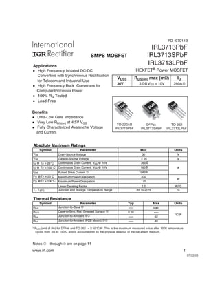
1. www.irf.com 1
07/22/05
IRL3713PbF
IRL3713SPbF
IRL3713LPbF
SMPS MOSFET
HEXFET® Power MOSFET
Notes through ‡ are on page 11
D2Pak
IRL3713SPbF
TO-220AB
IRL3713PbF
TO-262
IRL3713LPbF
Applications
Benefits
l Ultra-Low Gate Impedance
l Very Low RDS(on) at 4.5V VGS
l Fully Characterized Avalanche Voltage
and Current
l High Frequency Isolated DC-DC
Converters with Synchronous Rectification
for Telecom and Industrial Use
l High Frequency Buck Converters for
Computer Processor Power
l 100% RG Tested
l Lead-Free
VDSS RDS(on) max (mW) ID
30V 3.0@VGS = 10V 260A†
* RθJC (end of life) for D2Pak and TO-262 = 0.50°C/W. This is the maximum measured value after 1000 temperature
cycles from -55 to 150°C and is accounted for by the physical wearout of the die attach medium.
Symbol Parameter Units
VDS Drain-Source Voltage V
VGS Gate-to-Source Voltage V
ID @ TC = 25°C Continuous Drain Current, VGS @ 10V
ID @ TC = 100°C Continuous Drain Current, VGS @ 10V A
IDM Pulsed Drain Current c
PD @TC = 25°C Maximum Power Dissipation
PD @Tc = 100°C Maximum Power Dissipation
Linear Derating Factor W/°C
TJ, TSTG Junction and Storage Temperature Range °C
Symbol Parameter Typ Max Units
RθJC Junction-to-Case i ––– 0.45*
RqCS Case-to-Sink, Flat, Greased Surface f 0.50 –––
RθJA Junction-to-Ambient fi ––– 62
RθJA Junction-to-Ambient (PCB Mount) gi ––– 40
Thermal Resistance
Absolute Maximum Ratings
Max
260h
180h
1040h
30
± 20
2.2
170
°C/W
W
-55 to +175
330
PD - 97011B
2. IRL3713/S/LPbF
2 www.irf.com
Symbol Parameter Min Typ Max Units
V(BR)DSS Drain-to-Source Breakdown Voltage 30 ––– ––– V
∆V(BR)DSS/∆TJ Breakdown Voltage Temp. Coefficient ––– 0.027 ––– V/°C
––– 2.6 3.0
––– 3.3 4.0
VGS(th) Gate Threshold Voltage 1.0 ––– 2.5 V
––– ––– 50
––– ––– 20
––– ––– 100
Gate-to-Source Forward Leakage ––– ––– 200
Gate-to-Source Reverse Leakage ––– ––– -200
Symbol Parameter Min Typ Max Units
gfs Forward Transconductance 76 ––– ––– S
Qg Total Gate Charge ––– 75 110
Qgs Gate-to-Source Charge ––– 24 ––– nC
Qgd Gate-to-Drain ("Miller") Charge ––– 37 –––
QOSS Output Gate Charge 61 92
RG Gate Resistance 0.5 ––– 3.4 Ω
td(on) Turn-On Delay Time ––– 16 –––
tr Rise Time ––– 160 –––
td(off) Turn-Off Delay Time ––– 40 –––
tf Fall Time ––– 57 –––
Ciss Input Capacitance ––– 5890 –––
Coss Output Capacitance ––– 3130 –––
Crss Reverse Transfer Capacitance ––– 630 –––
Symbol Parameter Units
EAS mJ
IAR A
Symbol Parameter Min Typ Max Units
Continuous Source Current
(Body Diode)
Pulsed Source Current
(Body Diode)Ùh
––– 0.80 1.3
––– 0.68 –––
trr Reverse Recovery Time ––– 75 110 ns
Qrr Reverse Recovery Charge ––– 140 210 nC
trr Reverse Recovery Time ––– 78 120 ns
Qrr Reverse Recovery Charge ––– 160 240 nC
TJ = 125°C, IF = 30A, VR = 20V
di/dt = 100A/µs e
TJ = 125°C, IS = 30A, VGS = 0V e
TJ = 25°C, IF = 30A, VR = 0V
di/dt = 100A/µs e
Conditions
integral reverse
p-n junction diode.
TJ = 25°C, IS = 30A, VGS = 0V e
MOSFET symbol
showing the
–––
Conditions
VDS = 15V, ID = 30A
ID = 30A
VDS = 15V
VGS = 4.5V e
VGS = 0V
VDS = 15V
1530
46
VDS = 30V, VGS = 0V
VDS = 24V, VGS = 0V, TJ = 125°C
VGS = 20V
Conditions
VGS = 0V, ID = 250µA
Reference to 25°C, ID = 1mA
VGS = 10V, ID = 38A e
VGS = -20V
VGS = 4.5V, ID = 30A e
Max
VGS = 4.5V f
VDD = 15V
ID = 30A
RG = 1.8Ω
VDS = 24V, VGS = 0V
ƒ = 1.0MHz
VDS = VGS, ID = 250µA
Static @ TJ = 25°C (unless otherwise specified)
RDS(on) Static Drain-to-Source On-Resistance
IGSS
Diode Characteristics
Avalanche Characteristics
Dynamic @ TJ = 25°C (unless otherwise specified)
mΩ
IDSS Drain-to-Source Leakage Current µA
Avalanche CurrentÙ
Typ
–––
nA
ns
pF
Single Pulse Avalanche Energyd
IS ––– ––– 260 h
VGS = 0V, VDS = 15V
VSD Diode Forward Voltage V
A
ISM ––– ––– 1040 h
3. IRL3713/S/LPbF
www.irf.com 3
Fig 4. Normalized On-Resistance
Vs. Temperature
Fig 2. Typical Output CharacteristicsFig 1. Typical Output Characteristics
Fig 3. Typical Transfer Characteristics
0.1
1
10
100
1000
0.1 1 10 100
20µs PULSE WIDTH
T = 25 CJ °
TOP
BOTTOM
VGS
10V
8.0V
6.0V
4.5V
4.0V
3.3V
2.8V
2.5V
V , Drain-to-Source Voltage (V)
I,Drain-to-SourceCurrent(A)
DS
D
2.5V
1
10
100
1000
0.1 1 10 100
20µs PULSE WIDTH
T = 175 CJ °
TOP
BOTTOM
VGS
10V
8.0V
6.0V
4.5V
4.0V
3.3V
2.8V
2.5V
V , Drain-to-Source Voltage (V)
I,Drain-to-SourceCurrent(A)
DS
D
2.5V
1
10
100
1000
2.5 3.0 3.5 4.0 4.5
V = 15V
20µs PULSE WIDTH
DS
V , Gate-to-Source Voltage (V)
I,Drain-to-SourceCurrent(A)
GS
D
T = 25 CJ °
T = 175 CJ °
-60 -40 -20 0 20 40 60 80 100 120 140 160 180
0.0
0.5
1.0
1.5
2.0
T , Junction Temperature ( C)
R,Drain-to-SourceOnResistance
(Normalized)
J
DS(on)
°
V =
I =
GS
D
10V
260A
4. IRL3713/S/LPbF
4 www.irf.com
Fig 8. Maximum Safe Operating Area
Fig 6. Typical Gate Charge Vs.
Gate-to-Source Voltage
Fig 5. Typical Capacitance Vs.
Drain-to-Source Voltage
Fig 7. Typical Source-Drain Diode
Forward Voltage
0 40 80 120 160
0
2
4
6
8
10
12
14
Q , Total Gate Charge (nC)
V,Gate-to-SourceVoltage(V)
G
GS
I =D 30A
V = 6VDS
V = 15VDS
V = 24VDS
0.1
1
10
100
1000
0.2 0.4 0.6 0.8 1.0 1.2 1.4 1.6
V ,Source-to-Drain Voltage (V)
I,ReverseDrainCurrent(A)
SD
SD
V = 0 VGS
T = 25 CJ °
T = 175 CJ °
10
100
1000
10000
1 10 100
OPERATION IN THIS AREA LIMITED
BY RDS(on)
Single Pulse
T
T
= 175 C
= 25 C°
°J
C
V , Drain-to-Source Voltage (V)
I,DrainCurrent(A)I,DrainCurrent(A)
DS
D
10us
100us
1ms
10ms
1 10 100
VDS, Drain-to-Source Voltage (V)
100
1000
10000
100000
C,Capacitance(pF)
Coss
Crss
Ciss
VGS = 0V, f = 1 MHZ
Ciss = Cgs + Cgd, Cds SHORTED
Crss = Cgd
Coss = Cds+ Cgd
5. IRL3713/S/LPbF
www.irf.com 5
Fig 10a. Switching Time Test Circuit
VDS
90%
10%
VGS
td(on) tr td(off) tf
Fig 10b. Switching Time Waveforms
VDS
Pulse Width ≤ 1 µs
Duty Factor ≤ 0.1 %
RD
VGS
RG
D.U.T.
10V
+
-VDD
Fig 11. Maximum Effective Transient Thermal Impedance, Junction-to-Case
Fig 9. Maximum Drain Current Vs.
Case Temperature
0.001
0.01
0.1
1
0.00001 0.0001 0.001 0.01 0.1
Notes:
1. Duty factor D = t / t
2. Peak T =P x Z + T
1 2
J DM thJC C
P
t
t
DM
1
2
t , Rectangular Pulse Duration (sec)
ThermalResponse(Z)
1
thJC
0.01
0.02
0.05
0.10
0.20
D = 0.50
SINGLE PULSE
(THERMAL RESPONSE)
25 50 75 100 125 150 175
0
50
100
150
200
250
300
T , Case Temperature ( C)
I,DrainCurrent(A)
°C
D
LIMITED BY PACKAGE
6. IRL3713/S/LPbF
6 www.irf.com
QG
QGS QGD
VG
Charge
D.U.T.
VDS
IDIG
3mA
VGS
.3µF
50KΩ
.2µF12V
Current Regulator
Same Type as D.U.T.
Current Sampling Resistors
+
-
10 V
Fig 13b. Gate Charge Test CircuitFig 13a. Basic Gate Charge Waveform
Fig 12c. Maximum Avalanche Energy
Vs. Drain Current
Fig 12b. Unclamped Inductive Waveforms
Fig 12a. Unclamped Inductive Test Circuit
tp
V(BR)DSS
IAS
25 50 75 100 125 150 175
0
500
1000
1500
2000
2500
3000
Starting T , Junction Temperature ( C)
E,SinglePulseAvalancheEnergy(mJ)
J
AS
°
ID
TOP
BOTTOM
30A
38A
46A
RG
IAS
0.01Ωtp
D.U.T
LVDS
+
-
VDD
DRIVER
A
15V
20VVGS
7. IRL3713/S/LPbF
www.irf.com 7
P.W.
Period
di/dt
Diode Recovery
dv/dt
Ripple ≤ 5%
Body Diode Forward Drop
Re-Applied
Voltage
Reverse
Recovery
Current
Body Diode Forward
Current
VGS=10V
VDD
ISD
Driver Gate Drive
D.U.T. ISD Waveform
D.U.T. VDS Waveform
Inductor Curent
D =
P.W.
Period
+
-
+
+
+-
-
-
Fig 14. For N-Channel HEXFET® Power MOSFETs
* VGS = 5V for Logic Level Devices
Peak Diode Recovery dv/dt Test Circuit
ƒ
„
‚
RG
VDD
• dv/dt controlled by RG
• Driver same type as D.U.T.
• ISD controlled by Duty Factor "D"
• D.U.T. - Device Under Test
D.U.T
Circuit Layout Considerations
• Low Stray Inductance
• Ground Plane
• Low Leakage Inductance
Current Transformer
*
8. IRL3713/S/LPbF
8 www.irf.com
TO-220AB Part Marking Information
@Y6HQG@)
DIÃUC@Ã6TT@H7G`ÃGDI@ÃÅ8Å
UCDTÃDTÃ6IÃDSA Ã
GPUÃ8P9@Ã '(
6TT@H7G@9ÃPIÃXXÃ (Ã (( Q6SUÃIVH7@S
6TT@H7G`
GPUÃ8P9@
96U@Ã8P9@
`@6SÃÃ2Ã ((
GDI@Ã8
X@@FÃ (
GPBP
S@8UDAD@S
DIU@SI6UDPI6G
Note: P in assembly line
position indicates Lead-Free
TO-220AB Package Outline
Dimensions are shown in millimeters (inches)
10. IRL3713/S/LPbF
10 www.irf.com
TO-262 Part Marking Information
TO-262 Package Outline
Dimensions are shown in millimeters (inches)
6TT@H7G`
GPUÃ8P9@
S@8UDAD@S
DIU@SI6UDPI6G6TT@H7G@9ÃPIÃXXÃ (Ã ((
I‚‡r)ÃÅQÅÃvÃh††r€iy’Ãyvr
ƒ‚†v‡v‚Ãvqvph‡r†ÃÅGrhqA…rrÅ
DIÃUC@Ã6TT@H7G`ÃGDI@ÃÅ8Å GPBP
UCDTÃDTÃ6IÃDSG G
GPUÃ8P9@Ã '(
@Y6HQG@)
GDI@Ã8
96U@Ã8P9@
X@@FÃ (
`@6SÃÃ2Ã ((
Q6SUÃIVH7@S
Q6SUÃIVH7@S
GPBP
GPUÃ8P9@
6TT@H7G`
DIU@SI6UDPI6G
S@8UDAD@S
QSP9V8UÃPQUDPI6G
QÃ2Ã9@TDBI6U@TÃG@69AS@@
6Ã2Ã6TT@H7G`ÃTDU@Ã8P9@
X@@FÃ (
`@6SÃÃ2Ã ((
96U@Ã8P9@
OR
11. IRL3713/S/LPbF
www.irf.com 11
Repetitive rating; pulse width limited by max. junction temperature.
‚ Starting TJ = 25°C, L = 1.4mH, RG = 25Ω, IAS = 46A,VGS=10V.
ƒ Pulse width ≤ 400µs; duty cycle ≤ 2%.
„ This is only applied to TO-220A package.
… This is applied to D2Pak, when mounted on 1 square PCB ( FR-4 or G-10 Material ). For recommended footprint
and soldering techniques refer to application note #AN-994.
† Calculated continuous current based on maximum allowable junction temperature. Package limitation current is 75A.
‡ Rθ is measured at TJ approximately 90°C.
Notes:
Data and specifications subject to change without notice.
This product has been designed and qualified for the Industrial market.
Qualification Standards can be found on IR’s Web site.
IR WORLD HEADQUARTERS: 233 Kansas St., El Segundo, California 90245, USA Tel: (310) 252-7105
TAC Fax: (310) 252-7903
Visit us at www.irf.com for sales contact information. 07/05
D2Pak Tape Reel Information
Dimensions are shown in millimeters (inches)
3
4
4
TRR
FEED DIRECTION
1.85 (.073)
1.65 (.065)
1.60 (.063)
1.50 (.059)
4.10 (.161)
3.90 (.153)
TRL
FEED DIRECTION
10.90 (.429)
10.70 (.421)
16.10 (.634)
15.90 (.626)
1.75 (.069)
1.25 (.049)
11.60 (.457)
11.40 (.449)
15.42 (.609)
15.22 (.601)
4.72 (.136)
4.52 (.178)
24.30 (.957)
23.90 (.941)
0.368 (.0145)
0.342 (.0135)
1.60 (.063)
1.50 (.059)
13.50 (.532)
12.80 (.504)
330.00
(14.173)
MAX.
27.40 (1.079)
23.90 (.941)
60.00 (2.362)
MIN.
30.40 (1.197)
MAX.
26.40 (1.039)
24.40 (.961)
NOTES :
1. COMFORMS TO EIA-418.
2. CONTROLLING DIMENSION: MILLIMETER.
3. DIMENSION MEASURED @ HUB.
4. INCLUDES FLANGE DISTORTION @ OUTER EDGE.
12. Note: For the most current drawings please refer to the IR website at:
http://www.irf.com/package/