Transistor basics
•
1 gefällt mir•3,938 views

The study of the basics of electronics can be studied through the link http://bit.ly/2PPv0mv The transistor is a semiconductor device with three connections, capable of amplification in addition to rectification

Empfohlen
Weitere ähnliche Inhalte
Was ist angesagt?
Was ist angesagt? (20)
Ähnlich wie Transistor basics
Ähnlich wie Transistor basics (20)
Mehr von AtheenaPandian Enterprises
Mehr von AtheenaPandian Enterprises (20)
Kürzlich hochgeladen
Kürzlich hochgeladen (20)
Transistor basics
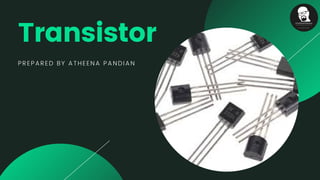
- 1. Transistor PREPARED BY ATHEENA PANDIAN
- 2. Crucial PointsDISCUSSION FLOW What is Transistor? Who invented Transistor? Symbol Structure Configuration Biasing Operation I-V Charecterisitic Curve Circuits Types Applications 1. 2. 3. 4. 5. 6. 7. 8. 9. 10. 11.
- 3. What is Transistor? - is a semiconductor device used to amplify or switch electronic signals and electrical power.
- 4. Inventors at Bells Telephone Labs, New Jersy, USA in 1947
- 5. Symbol b - base c - collector e - emittor
- 6. Construction placing n-type material between two p-type material which forms the pnp-transistor or by placing a p-type material between two n- type semiconductor which forms npn-transistor.
- 7. Doped semiconductor regions: the emitter region, the base region and the collector region. These regions are, respectively, p type, n type and p type in a PNP transistor, and n type, p type and n type in an NPN transistor. Structure The transistor is a three terminal device and consists of three distinct layers.
- 8. Configuration 3 TYPES OF CONFIGURATION Common Collector Common Base Common Emitter 1. 2. 3.
- 9. Common Collector Configuration POINT 1 The configuration in which the collector is common between emitter and base is known as CC configuration. POINT 2 The Input signal is applied to the base terminal and the output is taken from the emitter terminal
- 10. Common Collector Configuration OUTPUT CHARECTERISTICS Figure below shows the output characteristics for the CC configuration which exhibit the variations in IE against the changes in VCE for constant values of IB. INPUT CHARACTERISTICS Figure shows the input characteristics for CC configuration which describes the variation in IB in accordance with VCB, for a constant value of Collector-Emitter voltage, VCE.
- 11. Common Base Configuration POINT 1 The configuration in which the base is common between emitter and collector is known as CC configuration. POINT 2 Input - Emitter Base Output - Collector Base
- 12. Common Base Configuration INPUT CHARACTERISTICS Figure below shows the input characteristics of a CB configuration circuit which describes the variation of emitter current, IE with Base-Emitter voltage, VBE keeping Collector- Base voltage, VCB constant. OUTPUT CHARACTERISTICS The output characteristics of CB configuration show the variation of collector current, IC with VCB when the emitter current, IE is held constant. From the graph shown, the output resistance can be obtained as:
- 13. Common Emitter Configuration POINT 1 The configuration in which the emitter terminal is common for input and output circuit POINT 2 Input - Base Emitter Output - Collector Emitter
- 14. Common Emitter Configuration INPUT CHARACTERISTICS Figure shows the input characteristics for the CE configuration of transistor which illustrates the variation in IB in accordance with VBE when VCE is kept constant. OUTPUT CHARACTERISTICS The output characteristics of CE configuration are also referred to as collector characteristics. This plot shows the variation in IC with the changes in VCE when IB is held constant. From the graph shown, the output resistance can be obtained as:
- 15. TRANSISTOR BIASING Transistor Biasing is the process of setting a transistors DC operating voltage or current conditions to the correct level so that any AC input signal can be amplified correctly by the transistor
- 16. Operations
- 18. Transistor is an active component and that is establishing in all over electronic circuits. They are used as amplifiers and switching apparatus. As the amplifiers, they are used in high and low level, frequency stages, oscillators, modulators, detectors and in any circuit need to perform a function. 1. 2. 3. Application of Transistor
- 19. Thank you