SlideShare ist ein Scribd-Unternehmen logo
1 von 18
Downloaden Sie, um offline zu lesen
L
Laboration 2

Digita Circuit Design for Nan
al
noscale CMO
OS

HT2011

Layou and Physical V
ut
Verificati
ion
I this exerc you pra
In
cise
actice layout based on th Inverter t
he
that you cre
eated in the previous La Basic
ab.
f
functionality of the layo editor is explained. Schematic d
y
out
driven layou metal int
ut,
terconnects, vias and
w contacts are practic
well
ced. You al learn to execute the Design-Ru
lso
e
ule-Checking (DRC), La
g
ayout-vsS
Schematic, and Parasitic-Extraction using XRC.
a
u

1 Virtuos
1.
so	Layout
t	Editor	
S
Start the lay
yout editor
S
Start up the Virtuoso. Ch
V
hoose the sch
hematic view of the inve
w
erter that cre
eated in the p
previous exe
ercise
f
from the Library Manage window (F 1).
er
Fig.

Figure 1. Open the inve
O
erter schema
atic

S
Start the layo generatio tool from schematic window by s
out
on
m
w
selecting the menu Tool -> Design synthesis
e
l
- Layout XL The first time you star the tool yo are asked to create a n layout v
->
L.
t
rt
ou
d
new
view (Fig. 2)
).

Figure 2. Creating new layout view
w
w

1
L
Laboration 2

Digita Circuit Design for Nan
al
noscale CMO
OS

HT2011

T
Then, the lay
yout window is opened and the Lay Select W
w
yer
Window (LSW appears (
W)
(Fig. 3). The LSW is
e
u
used to selec which laye to display and edit. Fo example, to create wi in the M
ct
er
y
or
ires
Metal 1 drawi layer,
ing
s
select ME1, drw.

Figure 3. Layer Sele Window
3
ect

S
Some useful features of the LSW are the AV NV AS NS but
t
e
V
ttons. These buttons spec which layers in
cify
t layout wi
the
indow can be viewed or selected.
A All view
AV:
wable
Make all layers visib
ble
Use redra or CTRL-r for this to take affect
aw
o
N None vi
NV:
iewable
Make all layers excep the one cu
pt
urrently selected in the L
LSW invisible
Select oth layers in LSW to ma them visible as well
her
n
ake
Middle-c
clicking a lay in the LS toggles view on and off
yer
SW
v
Use redra or CTRL for this to take affect
aw
L-r
o
A all selectable
AS:
allows yo to select any layer
ou
a
Pin layer and instance (subcells) selection controlled by Inst and Pin at top of w
rs
)
y
n
window
N none sel
NS:
lectable
Turns off selection of layers (dar
f
rkens layer in LSW wind
n
dow)
Right-cli
icking a laye in the LSW toggles sel on and o
er
W
lect
off

2
L
Laboration 2

Digita Circuit Design for Nan
al
noscale CMO
OS

HT2011

G
Generate La
ayout
W
When the la
ayout editor is opened the first time the layout is empty. The layout is basically done by
t
e
t
instantiating the layout view of the cells from th design kit and wiring them up. I order to in
v
c
he
t,
g
In
nstantiate
a of the sch
all
hematic com
mponents in the layout window sele Design - Gen from Source or you can
w
ect
->
m
r
instantiate ea compone separatel by selecti it in the schematic w
ach
ent
ly
ing
window and place it in th layout
he
w
window usin Create -> Pick from Schematic. This brings o the layou Generation Form (Fig. 4).
ng
S
T
out
ut
n
.

Figure 4. Lay
F
yout Generat
tion Form

M
Make sure th IO pins are symbolic type and placed on th text layer M1_T as sh
hat
c
p
he
hown in figu 4 and
ure
p
press Apply. Press OK to generate th layout (Fig 5).
o
he
g.

3
L
Laboration 2

Digita Circuit Design for Nan
al
noscale CMO
OS

HT2011

Figure 5. Generated l ayout

B default only the outl
By
o
line of the components are displaye To view all layers, s
a
ed.
select the Op
ptions ->
D
Display or press e. Set th display stop level to 32 to view all layers of the compon
he
s
f
nents. In addition, in
t form cha
this
ange the X/Y Snap Spaci to 0.005. Also chang the Snap M
Y
ing
.
ge
Modes to an
nyAngle whic makes
ch
it possible to move the co
o
omponents freely (Fig. 6).
f
6

Figure 6. Display opt
6
tions

4
L
Laboration 2

Digita Circuit Design for Nan
al
noscale CMO
OS

HT2011

S
Select Optio -> DRD Edit and choose No
ons
D
otify for the Interactive Mode so that tool al
e
e
lerts you
a
automatically when viola
y
ating the des
sign rules (Fig. 7).

Figure 7. Set the DRD options
N
Now, in the layout edito you can see 4 pins an 2 transist
or,
s
nd
tors. Boundary layer is also visible (Fig. 8).
C
Click on eve component and press m to move it. Place all components within the b
ery
s
boundary. In order to
n
m
make the bou
undary non-s
selectable, do right-click on its layer prBoundary in LSW.
d
k
r
ry

Figure 8. Lines ind
e
dicate connec
ction of pins when movin componen
ng
nts.

S
Save your de
esign by usin the Desig → save co
ng
gn
ommand from the menu bar. To prev any une
m
vent
expected
l
loss of data, save your work regularly throughou the course of this labor
w
ut
ratory exercise.

5
L
Laboration 2

Digita Circuit Design for Nan
al
noscale CMO
OS

HT2011

C
Create inter
rconnect
W
When the components ar placed in the right pla you can create interc
re
t
ace,
connect usin metal wire and
ng
es
p
poly. Choos the approp
se
priate layer in LSW and select Creat -> path or press p to c
te
r
create connections.
Y can also choose Cre
You
o
eate-> Recta
angle to crea a rectangl instead of a path. The distance between
ate
le
f
e
t compone can be measured usi Window -> Cerate R
the
ents
m
ing
Ruler.
T connect the poly gat of two tr
To
t
tes
ransistors, ch
hoose P01 f
from LSW, and connec them by c
ct
creating a
p
path. In orde to intercon
er
nnect betwe layers yo need to c
een
ou
create a VIA or contact. For instanc if you
A
.
ce,
w to creat a VIA bet
want
te
tween the ga poly and Metal1, use the Create - contact o press o. Th size of
ate
M
->
or
he
t via is fix but you can adjust the number of rows and columns. In order to cr
the
xed,
t
o
n
reate a low r
resistance
c
contact it is necessary to use an array of contact Connect t drains of the transist
n
o
ts.
the
f
tors with Me 1 and
etal
l
locate one of the port rec
f
ctangles on it to be label as the ou
i
led
utport later. F 9 shows details of a possible
Fig.
s
l
layout around the inverte input and output. Note the port rec
er
e
ctangles in th Metal 1 layer.
he

PMOS

outpo
ort
inport

NMOS

Figure 9. Details of gat contact an In and Ou ports
D
te
nd
ut

B
Body and Su
ubstrate Co
onnections
T drawing in the Fig. 10 shows a sideview of a PMOS and NMOS put together.
The
g
1
s
d
t

6
L
Laboration 2

Digita Circuit Design for Nan
al
noscale CMO
OS

HT2011

Figure 10. Sideview of a CMOS
S

T PMOS transistors are placed in a separate NWELL w
The
a
n
which has to be connect to VCC. For this
ted
p
purpose, you should crea a contact between ME and NWE
u
ate
E1
ELL (Fig. 11).

Figu 11. Conn NWELL to the VCC
ure
nect
L

I the NWEL contact cannot be pl
If
LL
c
laced directly between t transistor it may be necessary t extend
the
rs
e
to
t NWELL by drawing for exampl an NWEL rectangle (
the
g
le
L
(Fig. 12). In continue, connect the S
Source of
t PMOS to the VCC.
the
o

VCC Pin
P

PMO
OS
Figure 12. Conne Source an N-WELL of the PMOS to the VCC
ect
nd
C

7
L
Laboration 2

Digita Circuit Design for Nan
al
noscale CMO
OS

HT2011

S
Similarly, yo should co
ou
onnect the su
ubstrate to th GND pin by creating a ME1 to P
he
n
g
PWELL contact (Fig.
1
13). What is the reaso that NW
i
on
Well and Psu
ubstrate sho
ould be con
nnected to t VDD an GND
the
nd
r
respectively?
?............................................................................
..........................................................
..............

Figure 13. Create a VIA to connect t substrate to GND
C
the

NMOS
N

GND Pin

Figure 14. Connecting substrate to the GND pin
1
e

A labels for pins
Add
f
T final step in layout is creating la
The
p
i
abels for pins. This is do in order f the Layo Versus Schematic
one
for
out
(
(LVS) tool to recognize the pins in the layout. Labels are created as text in the m
t
metal layer w
where the
p is locate using the menu Create->Label. This brings up the Create label form (
port
ed
T
p
e
(Fig. 15).

8
L
Laboration 2

Digita Circuit Design for Nan
al
noscale CMO
OS

Figure 15. Creating label for pins
F
l
T final inv
The
verter layout may look lik Fig. 16.
ke
S
Save the fina layout usin Design->
al
ng
>Save.

Figure 16 The final la
6.
ayout

9

HT2011
L
Laboration 2

Digita Circuit Design for Nan
al
noscale CMO
OS

HT2011

2 Design
2.
n	Check	Ru
ules	(DRC
C)	
W
When the lay
yout is finish it needs to be check for error according to the proc
hed
s
ked
rs
g
cess design r
rules. We
w use Assu to check the design. In the folder which you run Cadence make a fol
will
ura
r
lder for DRC runs.
C
mkdir LSI/LA
m
AB0/DRCs
R
Remember to erase the files in the te
o
f
emporary fol
lder after fin
nishing the D
DRC.
I the layout window, select Assura -> Run DR from the menu. In t run form you need t set the
In
t
a
RC
e
the
m
to
c
correct switc
ches and pr
rocess optio
ons. Fill in the DRC R
Run form to be exactly as Fig. 17 Select
o
y
7.
“
“umc90nm_D
DRC” as the Technology and “Optio
e
y
on13” for Ru Set.
ule

Figure 17. DR configura
F
RC
ation form

B default th UMC des
By
he
sign kit is co
onfigured to checks for all possible errors. Man errors, su as the
ny
uch
c
corner check die seal ring etc. are only meanin
k,
o
ngful when p
performing t final top
the
p-level verifi
ication of
t complete circuit. On top-level it is also nec
the
e
n
t
cessary to ha sufficien metal and poly cover
ave
nt
d
rage. The
D
DRC checks for coverag by defaul It is there
s
ge
lt.
efore conven
nient to filte out some of these wa
er
arnings in
t beginning In the DR configura
the
g.
RC
ation window click the S Switches button to configure wh DRC
w,
Set
s
hich
s
switches to use (Fig. 18).
u

10
L
Laboration 2

Digita Circuit Design for Nan
al
noscale CMO
OS

HT2011

Figure 18. Set switches f DRC
S
for

N
Now, press OK to start running the DRC. A Pro
O
r
D
ogress windo pops up a is visible as long as the DRC
ow
and
e
is running. By clicking the Watch lo file (Fig. 19) button y can watc the progre of the D
B
t
og
you
ch
ess
DRC. You
c review all of the er
can
a
rrors in Erro Layer Window (ELW and highl
or
W)
light each o them in th layout
of
he
w
window. Al spacing er
ll
rrors (betwe wires or other mate
een
r
erials) have to be fixed. You can u rulers
use
(
(press k) to modify the layout. Rule can be cl
m
l
ers
leared using shift + k. A
After modify
ying the layo rerun
out,
t DRC unt all errors are captured
the
til
a
d.

Figure 19. Watch log file
1
g

11
L
Laboration 2

Digita Circuit Design for Nan
al
noscale CMO
OS

HT2011

3
3‐	Layout	Versus	Schematic
c	(LVS)	
W
When the lay
yout is DRC clean, run the Layout Versus Sch
C
hematic (LVS) check, to check that all wires
o
a correctly connected, no vias are missing, all ports are in place an that all c
are
y
,
e
a
nd
components have the
c
correct value
es.
R
Remember th due to th bug in th tool/PDK, the pins ar not always recognized correctly. To avoid
hat
he
he
,
re
d
L
LVS problem a simple method is to place label with the n
ms,
o
ls
name of the p
ports over th metal con
he
nnected to
t
that.
I
Invoke the Assura LVS run form (F 20) usin the Assur
A
Fig.
ng
ra->Run LV menu. Co
VS
onfigure the LVS for
c
correct proce options in a similar way as the DRC and run the LVS. T LVS ca take a lon time to
ess
i
w
D
n
The
an
ng
f
finish, watch the progress in the out
h
tput log if necessary. W
n
When the LV is finishe the LVS complete
VS
ed
w
window open
ns.

Figure 20. Assura LVS r form
A
run

R LVS and if it asks to overwrite layout and source files, accept. The LVS debug window wi appear
Run
s
e
g
ill
a you can examine th results an discrepan
and
n
he
nd
ncies betwee the netlis and layou The LVS process
en
st
ut.
S
f
finishes whe the schem
en
matic and lay
yout match. In the wind
dow a numb of warnin are liste These
ber
ngs
ed.
c usually be ignored (F 21).
can
b
Fig.

12
L
Laboration 2

Digita Circuit Design for Nan
al
noscale CMO
OS

HT2011

Figure 21. LV complete window
F
VS
e

W
When the LV is finish you can open the LVS debug form ( Fig. 22). Sel an error and click th Open
VS
y
n
d
lect
r
he
T
Tool button. This brings up the corre LVS debu tool, for e
ect
ug
example the Parameter Missmatch t
e
tool.
M
Modify the layout or sch
hematic and rerun the LV until all e
r
VS
errors are cap
ptured (Fig. 23).

Figure 22. LVS debug form
g

Figure 23. LVS complet match
L
te

13
L
Laboration 2

Digita Circuit Design for Nan
al
noscale CMO
OS

HT2011

4
4‐	Hierarc
chical	Des
sign	
I this sectio we will use the invert cell conta
In
on,
u
ter
aining schem
matic and the layout to co
e
onstruct a di
igital
b
buffer. Creat a new sche
te
ematic cell view “digital
v
lBuffer”. Us the inverte symbol to create a dig
se
er
o
gital
b
buffer consis
sting of two cascaded inv
verters (Fig. 24).

Figure 24. Digital buffe using two cascaded inv
er
verters

C
Create a layo view for this circuit. The final lay
out
yout should look similar to Fig. 25. Remember t label
r
to
t pins acco
the
ording to their names in the schemati view.
t
ic

Figur 25. Final layout of the digital buffe
re
er

14
L
Laboration 2

Digita Circuit Design for Nan
al
noscale CMO
OS

HT2011

R
Rerun the DR and LVS to verify th the comp
RC
S
hat
plete circuit c
contains no e
errors. Use t rulers to measure
the
t outline of the final bu
the
uffer. What is the final area of your d
i
a
design?..........................................................
…
……......................................................................
....................
....................
....................
....................
...............

5
5‐	Parasit
tic	Extract
tion	
O
Open the As
ssura parasiti extraction run form (F 11) usin the menu Assura->Ru RCX in th layout
ic
n
Fig.
ng
un
he
e
editor (Fig. 26). In the extraction tab of RCX run form (F 26), spe
Fig.
ecify RC as the extract
s
tion type,
w
which means the parasiti resistance (R) and cap
s
ic
e
pacitance (C are extract You sho
C)
ted.
ould also spe
ecify VSS
a the referen node. Th press Ap and OK to run the p
as
nce
hen
pply
K
parasitic extraction.

Fi
igure 26. Par
rasitic extrac
ction form

N
Now, a new view av_ext
tracted is gen
nerated in th Library M
he
Manager.Ope it, parasitic elements are
en
v
visible over the layout (F 27).
t
Fig.

15
L
Laboration 2

Digita Circuit Design for Nan
al
noscale CMO
OS

HT2011

Figure 27. Parasitic elements of t digital bu
2
the
uffer

6
6‐	Simulating	using
g	the	extr
racted	vie
ew	
B creating a symbol for the digital buffer and make a test b ench, the fin circuit us
By
r
b
m
nal
sing the extra
acted
v
view can be simulated an compared to the stand
nd
d
dard schema
atic.

Figure 28. Dig
F
gital buffer t bench
test

S the chara
Set
acteristics of the pulse ge
f
enerator as th below.
he
16
L
Laboration 2

Digita Circuit Design for Nan
al
noscale CMO
OS

HT2011

tr= tf = 10p, Pulse width= 90p, Period= 190p
P
=

I the Analo Design Environment, set the sto time for t transient calculation to be 1ns. Run the
In
og
E
op
the
t
n
s
simulation to see the outp (B and C) and input (A) voltages.
o
put
C
M
Measure and record the output (C) rise time and fall time u
d
r
d
using the cro
osshair mark
kers. Rise tim of the
me
o
output is def
fined as the time taken for the outpu to rise from 10% of th final valu to 90% of the final
t
f
ut
m
he
ue
f
v
value………
………………
………………
………………
…………… ……………
………………
………………
………
D
Determine th pulse pro
he
opagation de
elay for out
tput signal B and C wi reference start of de
ith
e
elay time
m
measuremen at the 50% level of the Low-to-Hig change of the input si
nt
%
e
gh
f
ignal (A) res
spectively at the 50%
t
l
level of the High-to-Low change of the input sig
H
w
t
gnal.
P
Pulse propag
gation delay time for B:
tpLH,B =…………………
………………
……..

tpH =……… ……………
………………
……………
HL,B

a the mean time delay value td,B=( tpLH,B + tpH ) / 2 =……
and
n
=
…………………………
…………..
HL,B
P
Pulse propag
gation delay time for C:
tpLH,C =…………………
………………
……..

tpH =……… ……………
………………
……………
HL,C

a the mean time delay value td,C=( tpLH,B + tpH ) / 2 =……
and
n
=
…………………………
…………..
HL,C
T
Then, modify the switch list in the Se
fy
etup -> Envi
ironment to use extracte view by in
ed
nserting av_e
extracted
b
before schem
matic (Fig. 29). Change the plotting mode to App
t
m
pend and run the simulat
n
tion and com
mpare the
o
outputs.

Fig
gure 29. Swit list setup to simulate p
tch
parasitic extracted view

C
Calculate the mean time delay valu for B and C again. W
e
e
ue
d
What is the d
difference between dela in the
ays
c
case of schem
matic and ex
xtracted simu
ulation?
17
Laboration 2

Digital Circuit Design for Nanoscale CMOS

HT2011

Pulse propagation delay time for B using av_extracted view:
tpLH,B =…………………………………..

tpHL,B=……………………………………………

and the mean time delay value td,B=( tpLH,B + tpHL,B) / 2 =……………………………………..
Pulse propagation delay time for C using av_extracted view:
tpLH,C =…………………………………..

tpHL,C=……………………………………………

and the mean time delay value td,C=( tpLH,B + tpHL,C) / 2 =……………………………………..

7‐	Power	Calculation	
Add a capacitive load of 1fF to the output C. Plot the current of the capacitance. Measure the peak
current values when the output changes the value.
The NMOS transistor peak current value IdNMOS………………………………………………….
The PMOS transistor peak current value IdPMOS…………………………………………………..
Calculate the value of the electric charge Q which passes from the power source VDD to the lowest
potential VSS during one period of the input signal.
Q=…………………………………………………………………………………………………...
How much power does the inverter consume in the stationary state?
Ps=……………………………………………………………………………………………………
Calculate the switching power of the inverter? (Pd= cfv2)…………………………………………….
………………………………………………………………………………………………………..
How much is the total power consumption of the inverter? (P=Ps+Pd)……………………………….
………………………………………………………………………………………………………….

18

Weitere ähnliche Inhalte

Andere mochten auch

Efficient Layout Design of CMOS Full Subtractor
Efficient Layout Design of CMOS Full SubtractorEfficient Layout Design of CMOS Full Subtractor
Efficient Layout Design of CMOS Full SubtractorIJEEE
 
Semi-custom Layout Design and Simulation of CMOS NAND Gate
Semi-custom Layout Design and Simulation of CMOS NAND GateSemi-custom Layout Design and Simulation of CMOS NAND Gate
Semi-custom Layout Design and Simulation of CMOS NAND GateIJEEE
 
Automated layout synthesis tool for op amp
Automated layout synthesis tool for op ampAutomated layout synthesis tool for op amp
Automated layout synthesis tool for op ampNurahmad Omar
 
Pipeline processing - Computer Architecture
Pipeline processing - Computer Architecture Pipeline processing - Computer Architecture
Pipeline processing - Computer Architecture S. Hasnain Raza
 
Layout Design Analysis of CMOS Comparator using 180nm Technology
Layout Design Analysis of CMOS Comparator using 180nm TechnologyLayout Design Analysis of CMOS Comparator using 180nm Technology
Layout Design Analysis of CMOS Comparator using 180nm TechnologyIJEEE
 
Layout Design Analysis of SR Flip Flop using CMOS Technology
Layout Design Analysis of SR Flip Flop using CMOS TechnologyLayout Design Analysis of SR Flip Flop using CMOS Technology
Layout Design Analysis of SR Flip Flop using CMOS TechnologyIJEEE
 
Cadence layout Tutorial
Cadence layout TutorialCadence layout Tutorial
Cadence layout TutorialRajaSekar K
 
Microarchitecture
MicroarchitectureMicroarchitecture
Microarchitecturemeashi
 
Architecture of computer
Architecture of computerArchitecture of computer
Architecture of computerMubashar Islam
 
Electronic devices and circuit theory 11th ed
Electronic devices and circuit theory 11th edElectronic devices and circuit theory 11th ed
Electronic devices and circuit theory 11th edMobin Hossain
 
Vlsi cadence tutorial_ahmet_ilker_şin
Vlsi cadence tutorial_ahmet_ilker_şinVlsi cadence tutorial_ahmet_ilker_şin
Vlsi cadence tutorial_ahmet_ilker_şinilker Şin
 
Design and Fabrication of 4-bit processor
Design and Fabrication of  4-bit processorDesign and Fabrication of  4-bit processor
Design and Fabrication of 4-bit processorPriyatham Bollimpalli
 
Cmos fabrication by suvayan samanta
Cmos fabrication by suvayan samantaCmos fabrication by suvayan samanta
Cmos fabrication by suvayan samantaSuvayan Samanta
 
Analysis, Design and Implementation of 4-Bit Full Adder using FinFET
Analysis, Design and Implementation of 4-Bit Full Adder using FinFETAnalysis, Design and Implementation of 4-Bit Full Adder using FinFET
Analysis, Design and Implementation of 4-Bit Full Adder using FinFETrbl87
 
RISC-V Introduction
RISC-V IntroductionRISC-V Introduction
RISC-V IntroductionYi-Hsiu Hsu
 
Design and simulation of sayeh processor using verilog copy 1445752708332
Design and simulation of sayeh processor using verilog   copy 1445752708332Design and simulation of sayeh processor using verilog   copy 1445752708332
Design and simulation of sayeh processor using verilog copy 1445752708332akanksha sharma
 

Andere mochten auch (18)

Efficient Layout Design of CMOS Full Subtractor
Efficient Layout Design of CMOS Full SubtractorEfficient Layout Design of CMOS Full Subtractor
Efficient Layout Design of CMOS Full Subtractor
 
Semi-custom Layout Design and Simulation of CMOS NAND Gate
Semi-custom Layout Design and Simulation of CMOS NAND GateSemi-custom Layout Design and Simulation of CMOS NAND Gate
Semi-custom Layout Design and Simulation of CMOS NAND Gate
 
Automated layout synthesis tool for op amp
Automated layout synthesis tool for op ampAutomated layout synthesis tool for op amp
Automated layout synthesis tool for op amp
 
Pipeline processing - Computer Architecture
Pipeline processing - Computer Architecture Pipeline processing - Computer Architecture
Pipeline processing - Computer Architecture
 
Layout Design Analysis of CMOS Comparator using 180nm Technology
Layout Design Analysis of CMOS Comparator using 180nm TechnologyLayout Design Analysis of CMOS Comparator using 180nm Technology
Layout Design Analysis of CMOS Comparator using 180nm Technology
 
Layout Design Analysis of SR Flip Flop using CMOS Technology
Layout Design Analysis of SR Flip Flop using CMOS TechnologyLayout Design Analysis of SR Flip Flop using CMOS Technology
Layout Design Analysis of SR Flip Flop using CMOS Technology
 
Layout
LayoutLayout
Layout
 
Cadence layout Tutorial
Cadence layout TutorialCadence layout Tutorial
Cadence layout Tutorial
 
Microarchitecture
MicroarchitectureMicroarchitecture
Microarchitecture
 
Architecture of computer
Architecture of computerArchitecture of computer
Architecture of computer
 
Electronic devices and circuit theory 11th ed
Electronic devices and circuit theory 11th edElectronic devices and circuit theory 11th ed
Electronic devices and circuit theory 11th ed
 
Vlsi cadence tutorial_ahmet_ilker_şin
Vlsi cadence tutorial_ahmet_ilker_şinVlsi cadence tutorial_ahmet_ilker_şin
Vlsi cadence tutorial_ahmet_ilker_şin
 
Design and Fabrication of 4-bit processor
Design and Fabrication of  4-bit processorDesign and Fabrication of  4-bit processor
Design and Fabrication of 4-bit processor
 
Cmos fabrication by suvayan samanta
Cmos fabrication by suvayan samantaCmos fabrication by suvayan samanta
Cmos fabrication by suvayan samanta
 
Computer Architecture
Computer ArchitectureComputer Architecture
Computer Architecture
 
Analysis, Design and Implementation of 4-Bit Full Adder using FinFET
Analysis, Design and Implementation of 4-Bit Full Adder using FinFETAnalysis, Design and Implementation of 4-Bit Full Adder using FinFET
Analysis, Design and Implementation of 4-Bit Full Adder using FinFET
 
RISC-V Introduction
RISC-V IntroductionRISC-V Introduction
RISC-V Introduction
 
Design and simulation of sayeh processor using verilog copy 1445752708332
Design and simulation of sayeh processor using verilog   copy 1445752708332Design and simulation of sayeh processor using verilog   copy 1445752708332
Design and simulation of sayeh processor using verilog copy 1445752708332
 

Ähnlich wie Umc90 lab2 il2222

Ähnlich wie Umc90 lab2 il2222 (20)

Ads
AdsAds
Ads
 
Cadence tutorial lab_2_f16
Cadence tutorial lab_2_f16Cadence tutorial lab_2_f16
Cadence tutorial lab_2_f16
 
Cadence tutorial lab_2_f16
Cadence tutorial lab_2_f16Cadence tutorial lab_2_f16
Cadence tutorial lab_2_f16
 
Dtmf robot
Dtmf robotDtmf robot
Dtmf robot
 
Tutorial 2
Tutorial 2Tutorial 2
Tutorial 2
 
fpga 3D
fpga 3Dfpga 3D
fpga 3D
 
P spice tutorialhkn
P spice tutorialhknP spice tutorialhkn
P spice tutorialhkn
 
315925614 cadence-tutorial
315925614 cadence-tutorial315925614 cadence-tutorial
315925614 cadence-tutorial
 
Modeling seismic analysis_and_design_of_rc_building_10_story
Modeling seismic analysis_and_design_of_rc_building_10_storyModeling seismic analysis_and_design_of_rc_building_10_story
Modeling seismic analysis_and_design_of_rc_building_10_story
 
LCD WITH 8051.docx
LCD WITH 8051.docxLCD WITH 8051.docx
LCD WITH 8051.docx
 
IMPLEMENTING A DIGITAL MULTIMETER
IMPLEMENTING A DIGITAL MULTIMETERIMPLEMENTING A DIGITAL MULTIMETER
IMPLEMENTING A DIGITAL MULTIMETER
 
Using matlab simulink
Using matlab simulinkUsing matlab simulink
Using matlab simulink
 
Using matlab simulink
Using matlab simulinkUsing matlab simulink
Using matlab simulink
 
Simulations of a typical CMOS amplifier circuit using the Monte Carlo method
Simulations of a typical CMOS amplifier circuit using the Monte Carlo methodSimulations of a typical CMOS amplifier circuit using the Monte Carlo method
Simulations of a typical CMOS amplifier circuit using the Monte Carlo method
 
AllPosters
AllPostersAllPosters
AllPosters
 
Cmos uma
Cmos umaCmos uma
Cmos uma
 
Cmos uma
Cmos umaCmos uma
Cmos uma
 
Project_PPT_Presentation.ppt
Project_PPT_Presentation.pptProject_PPT_Presentation.ppt
Project_PPT_Presentation.ppt
 
Design System Design-ASM and Asynchronous Sequential Circuits
Design System Design-ASM and Asynchronous Sequential CircuitsDesign System Design-ASM and Asynchronous Sequential Circuits
Design System Design-ASM and Asynchronous Sequential Circuits
 
Auto cad ppt
Auto cad pptAuto cad ppt
Auto cad ppt
 

Kürzlich hochgeladen

1029-Danh muc Sach Giao Khoa khoi 6.pdf
1029-Danh muc Sach Giao Khoa khoi  6.pdf1029-Danh muc Sach Giao Khoa khoi  6.pdf
1029-Danh muc Sach Giao Khoa khoi 6.pdfQucHHunhnh
 
Mastering the Unannounced Regulatory Inspection
Mastering the Unannounced Regulatory InspectionMastering the Unannounced Regulatory Inspection
Mastering the Unannounced Regulatory InspectionSafetyChain Software
 
1029 - Danh muc Sach Giao Khoa 10 . pdf
1029 -  Danh muc Sach Giao Khoa 10 . pdf1029 -  Danh muc Sach Giao Khoa 10 . pdf
1029 - Danh muc Sach Giao Khoa 10 . pdfQucHHunhnh
 
BASLIQ CURRENT LOOKBOOK LOOKBOOK(1) (1).pdf
BASLIQ CURRENT LOOKBOOK  LOOKBOOK(1) (1).pdfBASLIQ CURRENT LOOKBOOK  LOOKBOOK(1) (1).pdf
BASLIQ CURRENT LOOKBOOK LOOKBOOK(1) (1).pdfSoniaTolstoy
 
Industrial Policy - 1948, 1956, 1973, 1977, 1980, 1991
Industrial Policy - 1948, 1956, 1973, 1977, 1980, 1991Industrial Policy - 1948, 1956, 1973, 1977, 1980, 1991
Industrial Policy - 1948, 1956, 1973, 1977, 1980, 1991RKavithamani
 
Separation of Lanthanides/ Lanthanides and Actinides
Separation of Lanthanides/ Lanthanides and ActinidesSeparation of Lanthanides/ Lanthanides and Actinides
Separation of Lanthanides/ Lanthanides and ActinidesFatimaKhan178732
 
Introduction to AI in Higher Education_draft.pptx
Introduction to AI in Higher Education_draft.pptxIntroduction to AI in Higher Education_draft.pptx
Introduction to AI in Higher Education_draft.pptxpboyjonauth
 
POINT- BIOCHEMISTRY SEM 2 ENZYMES UNIT 5.pptx
POINT- BIOCHEMISTRY SEM 2 ENZYMES UNIT 5.pptxPOINT- BIOCHEMISTRY SEM 2 ENZYMES UNIT 5.pptx
POINT- BIOCHEMISTRY SEM 2 ENZYMES UNIT 5.pptxSayali Powar
 
Accessible design: Minimum effort, maximum impact
Accessible design: Minimum effort, maximum impactAccessible design: Minimum effort, maximum impact
Accessible design: Minimum effort, maximum impactdawncurless
 
Measures of Central Tendency: Mean, Median and Mode
Measures of Central Tendency: Mean, Median and ModeMeasures of Central Tendency: Mean, Median and Mode
Measures of Central Tendency: Mean, Median and ModeThiyagu K
 
The basics of sentences session 2pptx copy.pptx
The basics of sentences session 2pptx copy.pptxThe basics of sentences session 2pptx copy.pptx
The basics of sentences session 2pptx copy.pptxheathfieldcps1
 
Privatization and Disinvestment - Meaning, Objectives, Advantages and Disadva...
Privatization and Disinvestment - Meaning, Objectives, Advantages and Disadva...Privatization and Disinvestment - Meaning, Objectives, Advantages and Disadva...
Privatization and Disinvestment - Meaning, Objectives, Advantages and Disadva...RKavithamani
 
Call Girls in Dwarka Mor Delhi Contact Us 9654467111
Call Girls in Dwarka Mor Delhi Contact Us 9654467111Call Girls in Dwarka Mor Delhi Contact Us 9654467111
Call Girls in Dwarka Mor Delhi Contact Us 9654467111Sapana Sha
 
Nutritional Needs Presentation - HLTH 104
Nutritional Needs Presentation - HLTH 104Nutritional Needs Presentation - HLTH 104
Nutritional Needs Presentation - HLTH 104misteraugie
 
Employee wellbeing at the workplace.pptx
Employee wellbeing at the workplace.pptxEmployee wellbeing at the workplace.pptx
Employee wellbeing at the workplace.pptxNirmalaLoungPoorunde1
 
Interactive Powerpoint_How to Master effective communication
Interactive Powerpoint_How to Master effective communicationInteractive Powerpoint_How to Master effective communication
Interactive Powerpoint_How to Master effective communicationnomboosow
 
mini mental status format.docx
mini    mental       status     format.docxmini    mental       status     format.docx
mini mental status format.docxPoojaSen20
 

Kürzlich hochgeladen (20)

1029-Danh muc Sach Giao Khoa khoi 6.pdf
1029-Danh muc Sach Giao Khoa khoi  6.pdf1029-Danh muc Sach Giao Khoa khoi  6.pdf
1029-Danh muc Sach Giao Khoa khoi 6.pdf
 
Código Creativo y Arte de Software | Unidad 1
Código Creativo y Arte de Software | Unidad 1Código Creativo y Arte de Software | Unidad 1
Código Creativo y Arte de Software | Unidad 1
 
Mastering the Unannounced Regulatory Inspection
Mastering the Unannounced Regulatory InspectionMastering the Unannounced Regulatory Inspection
Mastering the Unannounced Regulatory Inspection
 
1029 - Danh muc Sach Giao Khoa 10 . pdf
1029 -  Danh muc Sach Giao Khoa 10 . pdf1029 -  Danh muc Sach Giao Khoa 10 . pdf
1029 - Danh muc Sach Giao Khoa 10 . pdf
 
BASLIQ CURRENT LOOKBOOK LOOKBOOK(1) (1).pdf
BASLIQ CURRENT LOOKBOOK  LOOKBOOK(1) (1).pdfBASLIQ CURRENT LOOKBOOK  LOOKBOOK(1) (1).pdf
BASLIQ CURRENT LOOKBOOK LOOKBOOK(1) (1).pdf
 
TataKelola dan KamSiber Kecerdasan Buatan v022.pdf
TataKelola dan KamSiber Kecerdasan Buatan v022.pdfTataKelola dan KamSiber Kecerdasan Buatan v022.pdf
TataKelola dan KamSiber Kecerdasan Buatan v022.pdf
 
Industrial Policy - 1948, 1956, 1973, 1977, 1980, 1991
Industrial Policy - 1948, 1956, 1973, 1977, 1980, 1991Industrial Policy - 1948, 1956, 1973, 1977, 1980, 1991
Industrial Policy - 1948, 1956, 1973, 1977, 1980, 1991
 
Separation of Lanthanides/ Lanthanides and Actinides
Separation of Lanthanides/ Lanthanides and ActinidesSeparation of Lanthanides/ Lanthanides and Actinides
Separation of Lanthanides/ Lanthanides and Actinides
 
Staff of Color (SOC) Retention Efforts DDSD
Staff of Color (SOC) Retention Efforts DDSDStaff of Color (SOC) Retention Efforts DDSD
Staff of Color (SOC) Retention Efforts DDSD
 
Introduction to AI in Higher Education_draft.pptx
Introduction to AI in Higher Education_draft.pptxIntroduction to AI in Higher Education_draft.pptx
Introduction to AI in Higher Education_draft.pptx
 
POINT- BIOCHEMISTRY SEM 2 ENZYMES UNIT 5.pptx
POINT- BIOCHEMISTRY SEM 2 ENZYMES UNIT 5.pptxPOINT- BIOCHEMISTRY SEM 2 ENZYMES UNIT 5.pptx
POINT- BIOCHEMISTRY SEM 2 ENZYMES UNIT 5.pptx
 
Accessible design: Minimum effort, maximum impact
Accessible design: Minimum effort, maximum impactAccessible design: Minimum effort, maximum impact
Accessible design: Minimum effort, maximum impact
 
Measures of Central Tendency: Mean, Median and Mode
Measures of Central Tendency: Mean, Median and ModeMeasures of Central Tendency: Mean, Median and Mode
Measures of Central Tendency: Mean, Median and Mode
 
The basics of sentences session 2pptx copy.pptx
The basics of sentences session 2pptx copy.pptxThe basics of sentences session 2pptx copy.pptx
The basics of sentences session 2pptx copy.pptx
 
Privatization and Disinvestment - Meaning, Objectives, Advantages and Disadva...
Privatization and Disinvestment - Meaning, Objectives, Advantages and Disadva...Privatization and Disinvestment - Meaning, Objectives, Advantages and Disadva...
Privatization and Disinvestment - Meaning, Objectives, Advantages and Disadva...
 
Call Girls in Dwarka Mor Delhi Contact Us 9654467111
Call Girls in Dwarka Mor Delhi Contact Us 9654467111Call Girls in Dwarka Mor Delhi Contact Us 9654467111
Call Girls in Dwarka Mor Delhi Contact Us 9654467111
 
Nutritional Needs Presentation - HLTH 104
Nutritional Needs Presentation - HLTH 104Nutritional Needs Presentation - HLTH 104
Nutritional Needs Presentation - HLTH 104
 
Employee wellbeing at the workplace.pptx
Employee wellbeing at the workplace.pptxEmployee wellbeing at the workplace.pptx
Employee wellbeing at the workplace.pptx
 
Interactive Powerpoint_How to Master effective communication
Interactive Powerpoint_How to Master effective communicationInteractive Powerpoint_How to Master effective communication
Interactive Powerpoint_How to Master effective communication
 
mini mental status format.docx
mini    mental       status     format.docxmini    mental       status     format.docx
mini mental status format.docx
 

Umc90 lab2 il2222

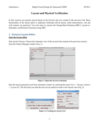
  • 1. L Laboration 2 Digita Circuit Design for Nan al noscale CMO OS HT2011 Layou and Physical V ut Verificati ion I this exerc you pra In cise actice layout based on th Inverter t he that you cre eated in the previous La Basic ab. f functionality of the layo editor is explained. Schematic d y out driven layou metal int ut, terconnects, vias and w contacts are practic well ced. You al learn to execute the Design-Ru lso e ule-Checking (DRC), La g ayout-vsS Schematic, and Parasitic-Extraction using XRC. a u 1 Virtuos 1. so Layout t Editor S Start the lay yout editor S Start up the Virtuoso. Ch V hoose the sch hematic view of the inve w erter that cre eated in the p previous exe ercise f from the Library Manage window (F 1). er Fig. Figure 1. Open the inve O erter schema atic S Start the layo generatio tool from schematic window by s out on m w selecting the menu Tool -> Design synthesis e l - Layout XL The first time you star the tool yo are asked to create a n layout v -> L. t rt ou d new view (Fig. 2) ). Figure 2. Creating new layout view w w 1
  • 2. L Laboration 2 Digita Circuit Design for Nan al noscale CMO OS HT2011 T Then, the lay yout window is opened and the Lay Select W w yer Window (LSW appears ( W) (Fig. 3). The LSW is e u used to selec which laye to display and edit. Fo example, to create wi in the M ct er y or ires Metal 1 drawi layer, ing s select ME1, drw. Figure 3. Layer Sele Window 3 ect S Some useful features of the LSW are the AV NV AS NS but t e V ttons. These buttons spec which layers in cify t layout wi the indow can be viewed or selected. A All view AV: wable Make all layers visib ble Use redra or CTRL-r for this to take affect aw o N None vi NV: iewable Make all layers excep the one cu pt urrently selected in the L LSW invisible Select oth layers in LSW to ma them visible as well her n ake Middle-c clicking a lay in the LS toggles view on and off yer SW v Use redra or CTRL for this to take affect aw L-r o A all selectable AS: allows yo to select any layer ou a Pin layer and instance (subcells) selection controlled by Inst and Pin at top of w rs ) y n window N none sel NS: lectable Turns off selection of layers (dar f rkens layer in LSW wind n dow) Right-cli icking a laye in the LSW toggles sel on and o er W lect off 2
  • 3. L Laboration 2 Digita Circuit Design for Nan al noscale CMO OS HT2011 G Generate La ayout W When the la ayout editor is opened the first time the layout is empty. The layout is basically done by t e t instantiating the layout view of the cells from th design kit and wiring them up. I order to in v c he t, g In nstantiate a of the sch all hematic com mponents in the layout window sele Design - Gen from Source or you can w ect -> m r instantiate ea compone separatel by selecti it in the schematic w ach ent ly ing window and place it in th layout he w window usin Create -> Pick from Schematic. This brings o the layou Generation Form (Fig. 4). ng S T out ut n . Figure 4. Lay F yout Generat tion Form M Make sure th IO pins are symbolic type and placed on th text layer M1_T as sh hat c p he hown in figu 4 and ure p press Apply. Press OK to generate th layout (Fig 5). o he g. 3
  • 4. L Laboration 2 Digita Circuit Design for Nan al noscale CMO OS HT2011 Figure 5. Generated l ayout B default only the outl By o line of the components are displaye To view all layers, s a ed. select the Op ptions -> D Display or press e. Set th display stop level to 32 to view all layers of the compon he s f nents. In addition, in t form cha this ange the X/Y Snap Spaci to 0.005. Also chang the Snap M Y ing . ge Modes to an nyAngle whic makes ch it possible to move the co o omponents freely (Fig. 6). f 6 Figure 6. Display opt 6 tions 4
  • 5. L Laboration 2 Digita Circuit Design for Nan al noscale CMO OS HT2011 S Select Optio -> DRD Edit and choose No ons D otify for the Interactive Mode so that tool al e e lerts you a automatically when viola y ating the des sign rules (Fig. 7). Figure 7. Set the DRD options N Now, in the layout edito you can see 4 pins an 2 transist or, s nd tors. Boundary layer is also visible (Fig. 8). C Click on eve component and press m to move it. Place all components within the b ery s boundary. In order to n m make the bou undary non-s selectable, do right-click on its layer prBoundary in LSW. d k r ry Figure 8. Lines ind e dicate connec ction of pins when movin componen ng nts. S Save your de esign by usin the Desig → save co ng gn ommand from the menu bar. To prev any une m vent expected l loss of data, save your work regularly throughou the course of this labor w ut ratory exercise. 5
  • 6. L Laboration 2 Digita Circuit Design for Nan al noscale CMO OS HT2011 C Create inter rconnect W When the components ar placed in the right pla you can create interc re t ace, connect usin metal wire and ng es p poly. Choos the approp se priate layer in LSW and select Creat -> path or press p to c te r create connections. Y can also choose Cre You o eate-> Recta angle to crea a rectangl instead of a path. The distance between ate le f e t compone can be measured usi Window -> Cerate R the ents m ing Ruler. T connect the poly gat of two tr To t tes ransistors, ch hoose P01 f from LSW, and connec them by c ct creating a p path. In orde to intercon er nnect betwe layers yo need to c een ou create a VIA or contact. For instanc if you A . ce, w to creat a VIA bet want te tween the ga poly and Metal1, use the Create - contact o press o. Th size of ate M -> or he t via is fix but you can adjust the number of rows and columns. In order to cr the xed, t o n reate a low r resistance c contact it is necessary to use an array of contact Connect t drains of the transist n o ts. the f tors with Me 1 and etal l locate one of the port rec f ctangles on it to be label as the ou i led utport later. F 9 shows details of a possible Fig. s l layout around the inverte input and output. Note the port rec er e ctangles in th Metal 1 layer. he PMOS outpo ort inport NMOS Figure 9. Details of gat contact an In and Ou ports D te nd ut B Body and Su ubstrate Co onnections T drawing in the Fig. 10 shows a sideview of a PMOS and NMOS put together. The g 1 s d t 6
  • 7. L Laboration 2 Digita Circuit Design for Nan al noscale CMO OS HT2011 Figure 10. Sideview of a CMOS S T PMOS transistors are placed in a separate NWELL w The a n which has to be connect to VCC. For this ted p purpose, you should crea a contact between ME and NWE u ate E1 ELL (Fig. 11). Figu 11. Conn NWELL to the VCC ure nect L I the NWEL contact cannot be pl If LL c laced directly between t transistor it may be necessary t extend the rs e to t NWELL by drawing for exampl an NWEL rectangle ( the g le L (Fig. 12). In continue, connect the S Source of t PMOS to the VCC. the o VCC Pin P PMO OS Figure 12. Conne Source an N-WELL of the PMOS to the VCC ect nd C 7
  • 8. L Laboration 2 Digita Circuit Design for Nan al noscale CMO OS HT2011 S Similarly, yo should co ou onnect the su ubstrate to th GND pin by creating a ME1 to P he n g PWELL contact (Fig. 1 13). What is the reaso that NW i on Well and Psu ubstrate sho ould be con nnected to t VDD an GND the nd r respectively? ?............................................................................ .......................................................... .............. Figure 13. Create a VIA to connect t substrate to GND C the NMOS N GND Pin Figure 14. Connecting substrate to the GND pin 1 e A labels for pins Add f T final step in layout is creating la The p i abels for pins. This is do in order f the Layo Versus Schematic one for out ( (LVS) tool to recognize the pins in the layout. Labels are created as text in the m t metal layer w where the p is locate using the menu Create->Label. This brings up the Create label form ( port ed T p e (Fig. 15). 8
  • 9. L Laboration 2 Digita Circuit Design for Nan al noscale CMO OS Figure 15. Creating label for pins F l T final inv The verter layout may look lik Fig. 16. ke S Save the fina layout usin Design-> al ng >Save. Figure 16 The final la 6. ayout 9 HT2011
  • 10. L Laboration 2 Digita Circuit Design for Nan al noscale CMO OS HT2011 2 Design 2. n Check Ru ules (DRC C) W When the lay yout is finish it needs to be check for error according to the proc hed s ked rs g cess design r rules. We w use Assu to check the design. In the folder which you run Cadence make a fol will ura r lder for DRC runs. C mkdir LSI/LA m AB0/DRCs R Remember to erase the files in the te o f emporary fol lder after fin nishing the D DRC. I the layout window, select Assura -> Run DR from the menu. In t run form you need t set the In t a RC e the m to c correct switc ches and pr rocess optio ons. Fill in the DRC R Run form to be exactly as Fig. 17 Select o y 7. “ “umc90nm_D DRC” as the Technology and “Optio e y on13” for Ru Set. ule Figure 17. DR configura F RC ation form B default th UMC des By he sign kit is co onfigured to checks for all possible errors. Man errors, su as the ny uch c corner check die seal ring etc. are only meanin k, o ngful when p performing t final top the p-level verifi ication of t complete circuit. On top-level it is also nec the e n t cessary to ha sufficien metal and poly cover ave nt d rage. The D DRC checks for coverag by defaul It is there s ge lt. efore conven nient to filte out some of these wa er arnings in t beginning In the DR configura the g. RC ation window click the S Switches button to configure wh DRC w, Set s hich s switches to use (Fig. 18). u 10
  • 11. L Laboration 2 Digita Circuit Design for Nan al noscale CMO OS HT2011 Figure 18. Set switches f DRC S for N Now, press OK to start running the DRC. A Pro O r D ogress windo pops up a is visible as long as the DRC ow and e is running. By clicking the Watch lo file (Fig. 19) button y can watc the progre of the D B t og you ch ess DRC. You c review all of the er can a rrors in Erro Layer Window (ELW and highl or W) light each o them in th layout of he w window. Al spacing er ll rrors (betwe wires or other mate een r erials) have to be fixed. You can u rulers use ( (press k) to modify the layout. Rule can be cl m l ers leared using shift + k. A After modify ying the layo rerun out, t DRC unt all errors are captured the til a d. Figure 19. Watch log file 1 g 11
  • 12. L Laboration 2 Digita Circuit Design for Nan al noscale CMO OS HT2011 3 3‐ Layout Versus Schematic c (LVS) W When the lay yout is DRC clean, run the Layout Versus Sch C hematic (LVS) check, to check that all wires o a correctly connected, no vias are missing, all ports are in place an that all c are y , e a nd components have the c correct value es. R Remember th due to th bug in th tool/PDK, the pins ar not always recognized correctly. To avoid hat he he , re d L LVS problem a simple method is to place label with the n ms, o ls name of the p ports over th metal con he nnected to t that. I Invoke the Assura LVS run form (F 20) usin the Assur A Fig. ng ra->Run LV menu. Co VS onfigure the LVS for c correct proce options in a similar way as the DRC and run the LVS. T LVS ca take a lon time to ess i w D n The an ng f finish, watch the progress in the out h tput log if necessary. W n When the LV is finishe the LVS complete VS ed w window open ns. Figure 20. Assura LVS r form A run R LVS and if it asks to overwrite layout and source files, accept. The LVS debug window wi appear Run s e g ill a you can examine th results an discrepan and n he nd ncies betwee the netlis and layou The LVS process en st ut. S f finishes whe the schem en matic and lay yout match. In the wind dow a numb of warnin are liste These ber ngs ed. c usually be ignored (F 21). can b Fig. 12
  • 13. L Laboration 2 Digita Circuit Design for Nan al noscale CMO OS HT2011 Figure 21. LV complete window F VS e W When the LV is finish you can open the LVS debug form ( Fig. 22). Sel an error and click th Open VS y n d lect r he T Tool button. This brings up the corre LVS debu tool, for e ect ug example the Parameter Missmatch t e tool. M Modify the layout or sch hematic and rerun the LV until all e r VS errors are cap ptured (Fig. 23). Figure 22. LVS debug form g Figure 23. LVS complet match L te 13
  • 14. L Laboration 2 Digita Circuit Design for Nan al noscale CMO OS HT2011 4 4‐ Hierarc chical Des sign I this sectio we will use the invert cell conta In on, u ter aining schem matic and the layout to co e onstruct a di igital b buffer. Creat a new sche te ematic cell view “digital v lBuffer”. Us the inverte symbol to create a dig se er o gital b buffer consis sting of two cascaded inv verters (Fig. 24). Figure 24. Digital buffe using two cascaded inv er verters C Create a layo view for this circuit. The final lay out yout should look similar to Fig. 25. Remember t label r to t pins acco the ording to their names in the schemati view. t ic Figur 25. Final layout of the digital buffe re er 14
  • 15. L Laboration 2 Digita Circuit Design for Nan al noscale CMO OS HT2011 R Rerun the DR and LVS to verify th the comp RC S hat plete circuit c contains no e errors. Use t rulers to measure the t outline of the final bu the uffer. What is the final area of your d i a design?.......................................................... … ……...................................................................... .................... .................... .................... .................... ............... 5 5‐ Parasit tic Extract tion O Open the As ssura parasiti extraction run form (F 11) usin the menu Assura->Ru RCX in th layout ic n Fig. ng un he e editor (Fig. 26). In the extraction tab of RCX run form (F 26), spe Fig. ecify RC as the extract s tion type, w which means the parasiti resistance (R) and cap s ic e pacitance (C are extract You sho C) ted. ould also spe ecify VSS a the referen node. Th press Ap and OK to run the p as nce hen pply K parasitic extraction. Fi igure 26. Par rasitic extrac ction form N Now, a new view av_ext tracted is gen nerated in th Library M he Manager.Ope it, parasitic elements are en v visible over the layout (F 27). t Fig. 15
  • 16. L Laboration 2 Digita Circuit Design for Nan al noscale CMO OS HT2011 Figure 27. Parasitic elements of t digital bu 2 the uffer 6 6‐ Simulating using g the extr racted vie ew B creating a symbol for the digital buffer and make a test b ench, the fin circuit us By r b m nal sing the extra acted v view can be simulated an compared to the stand nd d dard schema atic. Figure 28. Dig F gital buffer t bench test S the chara Set acteristics of the pulse ge f enerator as th below. he 16
  • 17. L Laboration 2 Digita Circuit Design for Nan al noscale CMO OS HT2011 tr= tf = 10p, Pulse width= 90p, Period= 190p P = I the Analo Design Environment, set the sto time for t transient calculation to be 1ns. Run the In og E op the t n s simulation to see the outp (B and C) and input (A) voltages. o put C M Measure and record the output (C) rise time and fall time u d r d using the cro osshair mark kers. Rise tim of the me o output is def fined as the time taken for the outpu to rise from 10% of th final valu to 90% of the final t f ut m he ue f v value……… ……………… ……………… ……………… …………… …………… ……………… ……………… ……… D Determine th pulse pro he opagation de elay for out tput signal B and C wi reference start of de ith e elay time m measuremen at the 50% level of the Low-to-Hig change of the input si nt % e gh f ignal (A) res spectively at the 50% t l level of the High-to-Low change of the input sig H w t gnal. P Pulse propag gation delay time for B: tpLH,B =………………… ……………… …….. tpH =……… …………… ……………… …………… HL,B a the mean time delay value td,B=( tpLH,B + tpH ) / 2 =…… and n = ………………………… ………….. HL,B P Pulse propag gation delay time for C: tpLH,C =………………… ……………… …….. tpH =……… …………… ……………… …………… HL,C a the mean time delay value td,C=( tpLH,B + tpH ) / 2 =…… and n = ………………………… ………….. HL,C T Then, modify the switch list in the Se fy etup -> Envi ironment to use extracte view by in ed nserting av_e extracted b before schem matic (Fig. 29). Change the plotting mode to App t m pend and run the simulat n tion and com mpare the o outputs. Fig gure 29. Swit list setup to simulate p tch parasitic extracted view C Calculate the mean time delay valu for B and C again. W e e ue d What is the d difference between dela in the ays c case of schem matic and ex xtracted simu ulation? 17
  • 18. Laboration 2 Digital Circuit Design for Nanoscale CMOS HT2011 Pulse propagation delay time for B using av_extracted view: tpLH,B =………………………………….. tpHL,B=…………………………………………… and the mean time delay value td,B=( tpLH,B + tpHL,B) / 2 =…………………………………….. Pulse propagation delay time for C using av_extracted view: tpLH,C =………………………………….. tpHL,C=…………………………………………… and the mean time delay value td,C=( tpLH,B + tpHL,C) / 2 =…………………………………….. 7‐ Power Calculation Add a capacitive load of 1fF to the output C. Plot the current of the capacitance. Measure the peak current values when the output changes the value. The NMOS transistor peak current value IdNMOS…………………………………………………. The PMOS transistor peak current value IdPMOS………………………………………………….. Calculate the value of the electric charge Q which passes from the power source VDD to the lowest potential VSS during one period of the input signal. Q=…………………………………………………………………………………………………... How much power does the inverter consume in the stationary state? Ps=…………………………………………………………………………………………………… Calculate the switching power of the inverter? (Pd= cfv2)……………………………………………. ……………………………………………………………………………………………………….. How much is the total power consumption of the inverter? (P=Ps+Pd)………………………………. …………………………………………………………………………………………………………. 18