2. fore, a permanent dipole is less likely related to the observed
behavior. The yield of the manipulation ͑directed movement͒
is low but we were able to manipulate a single Sb2 dimer on
the surface with a tunneling gap Ͼ0.5 nm. By analyzing the
force on an adsorbate we will show that the relative change
in energy for moving an induced Sb2 dipole on the surface
toward the tip is considerably smaller than the 0.5–1 eV
proposed earlier.7
However, the resulting change in energy
͑on the order of the thermal energy͒ is consistent with the
observed increase in Sb2 hopping rate.
II. SAMPLE PREPARATION
For most of the experiments we use p-type Si͑001͒ wafers
͑0.2 ⍀ cm͒. The oxide protected substrate is degassed in an
ultrahigh vacuum ͑UHV͒ system with a base pressure below
5ϫ10Ϫ11
mbar and flashed to 1500 K for several seconds.
The sample is cooled from 1100 K to room temperature at a
rate of approximately 1 K/s. We use a commercial variable
temperature STM. The samples are heated by passing a di-
rect current through the Si. This heating method is used for
the surface preparation, as well as for scans in the STM at
elevated temperature. Abouve 500 K Sb exhibits epitaxial
1ϫ2 growth on the 2ϫ1 Si͑001͒ surface.10
The Sb is deposited from an e-beam evaporator and the
coverages have been determined from the STM observations.
The quoted temperatures are measured with a pyrometer and
extrapolated below 750 K based on the heating current. The
extrapolation of the temperature versus heating current intro-
duces an appreciable error for temperatures below 500 K.
We reproduced the thermal hopping rate of the Sb2 dimers
͑at ‘‘noninvasive’’ scanning parameters, explained later͒ as a
criterion to reproduce the temperature settings.
Electrochemically etched tungsten tips are used for the
STM. The tips are degassed by electron bombardment after
loading into the UHV. Further cleaning and sharpening is
achieved by self-sputtering in neon as discussed in Ref. 11.
III. ANTIMONY ON Si„001…
Antimony evaporated from a source below 700 K onto a
room temperature Si surface deposits mainly as Sb4 clusters,
which can be converted into Sb2 dimers by annealing the
system at 460 K for several minutes. If the surface is further
annealed at 575 K the antimony self-assembles into short
epitaxial lines.10
Antimony diffuses preferentially orthogonal to the dimer
rows of the 2ϫ1 Si reconstruction with a diffusion barrier of
1.2 eV. The diffusion rate parallel to the Si dimer rows is
approximately 100 times lower.7
The Sb2 dimers are ob-
served to be immobile at room temperature but they start
hopping across Si dimer rows ͑as can be observed with the
STM͒ at temperatures as low as 400 K.
Scans done at large voltages with the STM enhance the
break up of the Sb4 clusters as well as induce hopping of Sb2
dimers to an adjacent Si dimer row12,13
already at room tem-
perature.
IV. MANIPULATION
The scanning of a STM can enhance the hopping of a Sb2
dimer on Si͑001͒ to a neighboring dimer row. To achieve
manipulation it is necessary to create a preferential direction
in this additional motion of the Sb2 dimer.
We have employed an asymmetric scan of the STM tip
over the substrate trying to break the symmetry. In this tech-
nique we use parameters for the feedback loop of the tunnel-
ing gap which are different for scanning in the left-to-right
direction compared to the right-to-left direction, as illustrated
in Fig. 1. One of these parameter sets should be invasive, i.e.,
move the dimer, while the other should interact as little as
possible ͑be noninvasive͒, allowing a net movement of the
adsorbate.
Adjustable parameters for the manipulation of an adsor-
bate are: the tunneling current (I0), bias voltage, the gain of
the feedback loop, as well as the scan speed. The hopping
rate of an adsorbate from one bonding site to the neighboring
one can be tuned by changing the temperature of the sub-
strate, resulting in a different distribution of energies within
the potential well of the adsorbate in the surface corrugation.
Tuning of the energy associated with the tip–adsorbate in-
teraction compared to the confinement of the adsorbate on
the surface should make it possible to find a parameter set,
which allows the manipulation of the Sb2 dimer. This, and
the introduction of an asymmetry, will be discussed in detail
below.
Figure 2 shows three subsequent scans at 500 K in which
we have used asymmetric scan parameters. The surface was
annealed at 575 K and therefore some epitaxial antimony
lines have formed. The small bars in the image indicate
which of the antimony dimers moved between subsequent
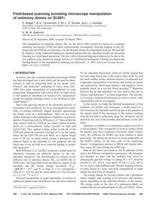
FIG. 1. Asymmetric tip scan. To manipulate the adsorbates on the surface
the tip is scanned with ‘‘invasive’’ parameters ͑e.g., 5 V 0.3 nA͒ in one
direction and then returned with the feedback settings of the gap used for
observations ͑e.g., 1.5 V 0.1 nA͒.
FIG. 2. Asymmetric scan of Sb on Si͑001͒. These three scans where taken
subsequently at 500 K after annealing the sample at 575 K. The tip is
scanned at Ϫ2 Vsubstrate and 0.1 nA from left to right and then returned at
Ϫ5 Vsubstrate and 0.3 nA from right to left. The bars indicate the position of
a dimer which moved in the following frame. Here we find net movement of
the free dimers along the tip sweep at high field.
660 Rogge et al.: Field-based STM manipulation of antimony dimers 660
J. Vac. Sci. Technol. B, Vol. 19, No. 3, MayÕJun 2001
3. scans. In these scans we observe a net movement of dimers
toward the left, the same direction as the tip scan with ‘‘in-
vasive’’ parameters ͑see the figure caption for details͒. In all
experiments ͑series of consecutive scans at elevated tempera-
ture͒ we exclusively observed free dimers moving, in con-
trast to Sb4 clusters or dimers, polymerized into an epitaxial
line.
From many experiments as in Fig. 2 statistics have been
established by averaging over many frames ͑with in total
about 100 dimers/frame͒ and analyzing the deviation from
the mean numbers of hopping dimers in the single scans of
the series. The schematic in Fig. 3 illustrates the percentage
of dimers hopping in a certain direction referenced to the
total number of dimers in a scan area. The error bars are
approximately one tenth of the quoted percentage. These sta-
tistics were obtained at 500 K for a noninvasive scan from
left-to-right ͑Ϫ1.5 V 0.1 nA fast feedback͒ and for an inva-
sive scan in the right-to-left direction ͑1.5 V 2 nA slow feed-
back, 5Iset current overshoot at the dimer͒. Due to poor tip
stability at positive substrate bias we do not have sufficient
data to discuss a field direction effect since most of the sta-
tistics were obtained with negative bias. However, in the few
runs with positive substrate bias we observed qualitatively
the same behavior as with negative bias. The left panel, of
the noninvasive scan, shows clearly that the preferential dif-
fusion direction of the Sb2 dimers is indeed orthogonal to the
dimer row. The right panel illustrates the mean movement
during asymmetric sweeps with the parameters mentioned
͑error approximately one-tenth of the quoted percentages͒.
We observed the preferential direction of motion now to be
along with the invasive tip movement ͑this can be reversed
as discussed below͒. Motion along the dimer rows has been
enhanced; it is as pronounced as the motion against the in-
vasive scan direction.
Figure 4 shows the total number of dimers hopping at
various tip fields for different scanning sessions. In this case
we used symmetric scans with identical parameters in both
directions. The field quoted is defined as the bias voltage
divided by the tip–surface distance resulting in an upper
limit of the actual field. The absolute tip–surface distance
was estimated by fits of the current versus relative tip height
measurements for the voltages used. The three curves were
taken for an identical sample with the same tip on different
days with fresh surface preparation each time. All control-
lable parameters remained the same yet the onset of hopping
is substantially different.
The relative net-hopping rate for a large number of ex-
periments is shown in Fig. 5 where a positive value denotes
the fraction of dimers moving in the same direction as the
invasive scan, ⌬ϭ(NleftϪNright)/(NleftϩNright). The error
bar for these numbers is at most 10% determined in the same
way as mentioned in the context of Fig. 3. It is important to
note that each data point outside Ϯ10% corresponds to a
series of scans which all had a significant net movement of
dimers in one direction.
Slow feedback ͑low loop gain͒ as well as high scan speed
can be used to create an additional increase in the field close
FIG. 3. Schematic shows the hopping rates for an observational ͑left͒ and an
invasive ͑right͒ scan at 500 K. The lines indicate the direction of the sub-
strate dimer rows which run parallel to the Sb dimer. The percentages indi-
cate the relative number of dimers which moved in a certain direction during
a scan ͑typically 80–120 dimers in the scan field, averaged over many
scans͒. The noninvasive scan was done at Ϫ1.5 V 0.1 nA; the invasive one
at rightwards Ϫ1.5 V 0.1 nA and leftwards Ϫ1.5 V 2 nA 0.05% loop gain.
FIG. 4. Tip induced motion. The percentage of total hops is the sum of
hopping events in any direction divided by the total number of dimers in the
scan range ϫ100%. The quantity is plotted vs tip field for three different
scan sessions of the same sample and tip resulting in three different slopes.
This shows that the tip induced hopping does not simply depend on the field.
We suggest that different tip terminations change the gradient of the field
resulting in a scaling of the slopes.
FIG. 5. Net hopping direction. The graph shows the relative motion of Sb2 ,
⌬ϭ (NleftϪNright)/(NleftϩNright), for various tip fields. The symbols denote
ranges of the tunnel current used during the invasive scans ͑right to left͒ and
so a positive ⌬ denotes motion along with the invasive sweep. Open sym-
bols indicate low loop-gain scans. The data were not all taken with the same
sample and tip but all controllable parameters were kept constant.
661 Rogge et al.: Field-based STM manipulation of antimony dimers 661
JVST B - Microelectronics and Nanometer Structures
4. to the dimer. In the low loop-gain experiments the peak cur-
rent was used to determine the field listed in Fig. 5 ͑open
symbols͒. The tip does not make contact with the dimer
͑verified by the current trace during the manipulation͒, hence
this technique is also long range.
A remarkable observation is that the induced motion of
the Sb2 dimers can be along with as well as against the
direction of the invasive scan. There is no obvious trend with
respect to the applied field ͑bias/height͒. However, the aver-
age of the low loop-gain experiments ͑higher current ‘‘be-
fore’’ the tip passes the center of the Sb2 dimer͒ shows a
tendency for hopping toward the tip, open symbols in Fig. 5.
We think that a low loop gain breaks the symmetry of the
tip–adsorbate system by creating a larger field when the tip
first encounters the ad-dimer compared to when it has passed
over it. This will be discussed in more detail in Sec. V in the
context of the tip/adsorbate interaction model.
We have investigated the possibility of manipulating a
single dimer, by using an asymmetric sweep with invasive
parameters solely over only one ad-dimer and an noninva-
sive scan in the larger scan field for observation. As shown in
Fig. 6 the field is localized enough even at the invasive pa-
rameters used ͑Ϫ5 V, 0.2 nA͒ to move the single ad-dimer.
Affecting only one dimer is quite reproducible but the yield
of these manipulations is not very high. This is consistent
with the small fraction of dimers hopping ͑a few out of 100͒
in full scans as indicated by the percentages in Fig. 3. We
present no quantitative yield for the single dimer manipula-
tion since we do not have enough events for accurate statis-
tics.
Going to higher fields was marginally possible in experi-
ments on single dimers ͑not for the statistical approach based
on many asymmetric scans͒. High fields ͑large tunneling cur-
rent at a high gap voltage, e.g., Ͼ3 nA, 5 V͒ very frequently
result in a severe change of the tip geometry or field evapo-
ration of Si. In these experiments we did not observe a high
yield of directed manipulation.
V. TIP–ADSORBATE INTERACTION
An ‘‘impact’’-based mechanism seems unlikely for Sb2
since the dimer appears in the STM to be only approximately
0.13 nm high. The currents required for stabilizing the tip at
this separation are enormous and would destroy tip and/or
substrate on the nanometer scale. Therefore we did not
implement this technique. The low loop-gain experiments
mentioned above still showed a finite maximum current
(Ͻ20 nA) close to the dimer, hence no contact was made.
Transfer of a Sb2 dimer from the surface to the tip was not
observed in any of our experiments ͑no missing dimers in
large series of consecutive scans͒ unless the surface was de-
stroyed.
We will discuss a model for the observed behavior based
on the force due to the electric field of the STM tip. The
tip–adsorbate interaction can be modeled by a dipole in the
field of a point charge. A spherical tip of radius R can be
represented as a point charge of such a magnitude to have an
equipotential sphere of radius R at the potential of the bias
voltage. This radius R is thus approximately the radius of
curvature of the actual tip. Zero potential is defined at a
depth in the silicon comparable to the size of the depletion
layer. The components normal and parallel to the surface of
such a field are plotted in Fig. 7.
The adsorbate is modeled as an isotropic linearly polariz-
able dipole p„E…ϭ␣E, where ␣ is the polarizability. The
energy W of an induced dipole in the field E of a point
charge is Wϭp"E. This can be written as a function of the
in-plane distance (r) to the point below the tip:
W͑r,z͒ϭϪ␣
ͩ V0
1
R
Ϫ
1
Rϩhϩd
ͪ
2
•ͩ r2
͑r2
ϩ͑Rϩh͒2
͒3
ϩ
͑RϩhϪz͒2
͑r2
ϩ͑RϩhϪz͒2
͒3ͪ.
FIG. 6. Single dimer manipulation. The left STM scan shows Sb2 dimers on
several Si͑001͒ terraces. An asymmetric tip scan was employed in the box
over one dimer. The leftward sweep was at Ϫ5 V 0.2 nA and the rightward
sweep identical to the observation parameters of Ϫ1.5 V 0.1 nA. After ten
lines of this sweep the surface is rescanned. The dimer moved toward the
step edge along the direction of the invasive scan and one dimer row ͑its
preferential direction͒. The neighboring dimers did not move. This scan was
done at 500 K where some diffusion occurs. The experiment demonstrates
that the field is local enough to manipulate a single dimer.
FIG. 7. Cylindrical components of the field of a spherical tip. charge. The
dashed curve represent the field normal to the substrate and the solid curve
the in-plane component both as a function of in-plane distance, r, to the tip
͑Rtipϭ5 nm, htipϪsampleϭ1 nm, Vbiasϭ3 V, ddepletionϭ10 nm). The in-plane
term shows a maximum in magnitude which is not directly under the tip.
662 Rogge et al.: Field-based STM manipulation of antimony dimers 662
J. Vac. Sci. Technol. B, Vol. 19, No. 3, MayÕJun 2001
5. Here h is the tip surface separation, d is the width of the
depletion layer, and R is the radius of curvature of the tip.
The energy term W is cylindrically symmetric so only the
radial distance of the adsorbate to the tip and the motion of
the tip are important for the manipulation.
A rough estimate for the polarizability ␣ is the value for a
free antimony atom ␣ϭ1.1ϫ10Ϫ39
C m2
/V.8
In general an
adsorbate on the surface is expected to have a polarizability
different from the free specimen ͑atom, dimer͒. Based on
their diffusion studies Whitman et al.6
argued that the polar-
izability of Cs is considerably larger on the InSb͑110͒ sur-
face than expected. We have done preliminary quantum
chemical calculations to find ␣ of a Sb2Si7H10 cluster. The
structure of this cluster is based on a single Sb2 dimer on the
Si͑001͒ 2ϫ1 reconstruction. The Sb atoms are bonded to-
gether and to two Si atoms each. Remaining Si dangling
bonds are terminated by hydrogen atoms. The approximate
polarizability of this cluster is 8.8ϫ10Ϫ38
C m2
/V, with a
permanent dipole of 2.4ϫ10Ϫ30
C m orthogonal to the
Sb–Sb and to the Si surface. For comparison, replacing the
Sb with H leads to 6.0ϫ10Ϫ38
C m2
/V and 0.4ϫ10Ϫ30
C m.
The energy available to move the induced dipole in-plane
is set to be the energy difference of the initial and final po-
sition dWϭW(rinit)ϪW(rfinal). As shown in Fig. 7 the in-
plane component of the field is considerably smaller than the
normal component and goes to zero below the tip. Figure 8
displays the energy gained by displacing the dipole 0.4 nm in
the plane toward the tip. For comparison the energy gained
by displacing an induced Sb2 dipole 0.4 nm toward the tip
normal to the plane is plotted in Fig. 9 as a function of
in-plane distance to the tip for various tip radii.
The energy change due to the field of the STM tip has to
be compared to the corrugation potential of the surface. The
Sb2 dimers are confined to the chains ͑0.76 nm spacing͒ of
the Si substrate by a potential barrier of 1.2 eV.7
The dis-
placement of the adsorbate used in the plots ͑0.4 nm͒ is
motivated by a simple potential landscape: 1.2 eV confine-
ment from the center of the chain to the center of the *
chain. If the potential gain due to a 0.4 nm displacement is
greater than 1.2 eV the Sb2 dimer would hop onto the next Si
chain ignoring the aid of thermal occupation of higher
energy levels. However, assumption of an Arrhenius law for
the hopping rate, ⍀ exp(ϪE/kT), leads to the following ex-
pression for the necessary change in barrier height to double
the hopping rate: ⌬EϭkT ln 2ϭ27 meV͉450 K .
Figure 10 shows the potential change for a permanent
dipole in a field. The same displacement of 0.4 nm was cho-
sen for comparison with Fig. 8. For the field direction used
the curves reflect a repulsive force directly below the tip in
contrast to the force on an induced dipole. Furthermore, in
contrast to the induced dipole the force changes sign at a
distance comparable to the tip radius of curvature plus the tip
height over the surface, Rϩh. The energy associated with
displacing a permanent dipole of the magnitude expected for
FIG. 8. Change in energy for a 0.4 nm in-plane displacement of an induced
dipole ͑Sb2 dimer͒. The solid curve represents a tip radius of curvature of
Rϭ0.3 nm, the dashed curve Rϭ1 nm, and the dotted curve Rϭ5 nm ͑tip–
sample distance of hϭ1 nm ͑polarizability 8.8ϫ10Ϫ38
C m2
/V, Vbias
ϭ3 V, ddepletionϭ10 nm). The model results in an attractive force with a
maximum at a distance approximately half of the radius of R.
FIG. 9. Change in energy for a 0.4 nm displacement normal to the surface of
an induced dipole ͑Sb2 dimer͒. Parameters are identical to the curves in Fig.
8. The model results in an attractive force with a maximum directly below
the tip. The 0.4 nm normal to the surface was chosen for comparison to the
displacement of one dimer row in the plane.
FIG. 10. Change in energy for a 0.4 nm displacement of a permanent dipole,
pϭ2.4ϫ10Ϫ30
C m ͑other parameter identical to the other plots͒. Except for
the region very close to the origin ͑set by the tip radii͒ the potential change
is overall attractive ͑or repulsive for opposite field direction͒ with a mini-
mum slightly further way from the origin compared to the induced dipole.
663 Rogge et al.: Field-based STM manipulation of antimony dimers 663
JVST B - Microelectronics and Nanometer Structures
6. Sb2 is at the most a few meVӶkT in contrast to the induced
dipole. Hence, the contribution from a permanent dipole is
small compared to the potential of the surface corrugation. In
contrast to Sb, Cs is an adsorbate with a large permanent
dipole compared to the induced dipole.6
The energy gain of a Sb2 dimer hopping one dimer row
closer to the tip in the case of an induced dipole as shown in
Fig. 8 is considerably lower compared to the same displace-
ment normal to the plane at shown in Fig. 9. Furthermore,
the in-plane movement shows a maximum in force at a dis-
tance of roughly half the tip diameter in contrast to the nor-
mal component with a maximum exactly below the tip. In
contrast to the permanent dipole the coupling of the normal
and parallel component in the energy term of the induced
dipole results in an overall attractive potential.
The depletion depth for Figs. 7–10 was chosen to be 10
nm without taking into account the effect of the dielectric or
a ground plane on the field distribution at the adsorbate. The
depth was only used to find the magnitude of the point
charge. Placing the zero potential reference at infinity will
lower the maximum energy in the dW plots by a factor of 2.
Placing the zero reference at the surface will increase the
energy available for a displacement of an induced dipole by
a factor of 150. However, this assumption is unphysical since
it implies no depletion layer and a metallic surface with a
nonzero in-plane field component.
The large dielectric constant of Si, ⑀Siϭ12, will cause a
larger in-plane component of the electric field. This will af-
fect the Sb2 dimer on the surface since the induced field of
the dielectric will partly extend into the vacuum. The field
distortion due to ionized dopants should be small, since we
work with fairly low doped substrates, and the amount of
charge at the tip even with a depletion zone reaching to in-
finity is larger than ten electrons. The dominant unknowns
are the polarizability of the Sb2 dimer on the Si͑001͒ surface
and the tip radius and shape.
It is necessary to investigate the importance of vibrational
heating as a source of the Sb2 manipulation. Local heating
due to the STM tip can cause adsorbate motion as discussed
in Ref. 14. Heating due to inelastic tunneling was success-
fully applied to two experimental systems: xenon on a metal
surface at low temperature and hydrogen on Si at room tem-
perature. The tunneling current creates in both cases a sub-
stantial temperature increase of the adsorbate compared to
the substrate temperature. The model discussed in Ref. 14
can also be applied to Sb2 on Si. The atomic mass of Sb is
similar to Xe and so the same vibrational frequency ͑2.5
meV͒ should be a good approximation. For this low fre-
quency coupling to phonons should be the dominant process
that limits the lifetime of the excited state. Using the speed
of sound and density of Si and the atomic mass of Sb we find
a vibrational damping rate for Sb on Si of 1/15 ps ͑slightly
faster than in the case of xenon͒. Following the argument of
Ref. 14 this results in a temperature elevation of the adsor-
bate of Ϸ0.15 K at 300 K for a current of 5 nA with a large
inelastic tunneling fraction of 10Ϫ3
. The effect is much
stronger for hydrogen: the low mass results in a high fre-
quency vibration, 2084 cmϪ1
,14
with a much longer lifetime
since this is above the highest phonon modes of the sub-
strate. At room temperature vibrational heating of Sb on Si
͑0.012 meV͒ is a small effect compared to the change in
energy due to the tip–dipole interaction ͑10 meV for a mac-
roscopic tip͒.
VI. DISCUSSION
The energy available for manipulation due to an electric
field-based interaction between tip and adsorbate is only on
the order of the thermal energy leading to a low probability
of directed hopping. If the enhanced hopping rate due to the
tip is small compared to the existing diffusion the asymmetry
introduced due to the tip motion will not lead to directed
motion since the hopping rate is too low to follow the tip.
The change in potential landscape needs to be local as indi-
cated by the 0.4 nm shift used in the calculations above. If
the potential barrier of the corrugation is lowered on both
sides of the adsorbate with respect to the tip position only a
larger total hopping rate is to be expected as observed in Fig.
4. As shown in Fig. 8 an ultrasharp tip of Rϭ0.3 nm can lead
to a locally large enough field to cause directed manipulation
but already a tip of Rϭ5 nm leads to a low gradient causing
a lowering of the barriers with a small asymmetry. Thus,
only an ultrasharp tip can lead to directed hopping.
A cylindrically symmetric potential/force due the tip, Fig.
8, can lead to an anisotropy in the manipulation due to the
motion of the tip. If the dimer has hopped along the direction
of tip motion an additional hopping event is more probable
than in the case where the dimer has hopped in another di-
rection. This asymmetry will appear if the attraction of the
tip is strong enough to drag the adsorbate along. An en-
hanced isotropic hopping rate ͑ignoring preferred directions
due to the substrate͒ is the result of a weak interaction since
the adsorbates cannot follow the tip. This symmetry can be
broken to an extent by a low loop-gain scan, enhancing the
field on one side of the dimer as discussed above. The force
on an induced dipole is attractive as shown in Fig. 8, result-
ing in a hop toward the tip which is consistent with the
negative average of the relative hopping rate ⌬ in Fig. 5. The
high loop-gain experiments have a positive average indicat-
ing a small tendency to hop with the tip as argued in the
beginning of the paragraph. We still need to explain the ori-
gin of the large scatter in Fig. 5.
There is another way to create an asymmetry in the direc-
tion of adsorbate hopping. If the termination of the tip is not
symmetric, the gradient on the ‘‘front side’’ of the tip can be
considerably different from the ‘‘backside’’ of the tip. This
situation would either favor an invasive front- or backside of
the tip breaking the symmetry of adsorbate movement. The
adsorbate can in principle either hop toward the tip before
the tip passes over it or afterwards, resulting in a motion with
or against the tip direction. If the tip is symmetric and the
probability for a second hop low this will lead to zero net
movement. However, if the tip is not symmetric, the force of
the front side of the tip can be different from the backside.
664 Rogge et al.: Field-based STM manipulation of antimony dimers 664
J. Vac. Sci. Technol. B, Vol. 19, No. 3, MayÕJun 2001
7. This will favor motion along with, or against, the direction of
motion of the tip.
The magnitude of the gradient seen by the Sb2 dimer will
be dominated by the last few atoms on the effective apex of
the tip, the microtip. A microtip, which extends only few
atoms, dominates the field gradient on the few nm length
scale. The local field is not screened on the length scale of
the microtip deviation from the macroscopic tip, as has been
shown by calculations15
of the field profile of a ‘‘blunt’’ tip
with an extension of atomic dimensions. At the current time
microtips cannot be fabricated, they are created by micro-
scopic changes of the tip during scanning like a rearrange-
ment of the tip apex or adsorption of particles from the sur-
face onto the tip. It may also already be altered after
establishing the initial tunneling current due to the close
proximity to the surface ͑large current, feedback overshoot͒.
This explains that the gradient of the tip field, which is de-
termined by the termination of the tip, cannot be reproduced
in a controlled way. Changes in the microscopic tip termina-
tion can be observed by field ion microscopy.16
We did not
have this technique at our disposal but such a study could
further confirm this model. A microtip with a certain sym-
metry will dominate a series of scans resulting in net move-
ment or just enhanced hopping, as shown in Fig. 5. This lack
of control over the symmetry of the microtip can thus ex-
plain the large scatter observed in the net hopping direction.
On substrates with a smaller corrugation potential a field-
based manipulation technique also does not lead to atomic
scale manipulation. In this case the confining potential of the
adsorbate on the surface is smaller. Nevertheless, an atomi-
cally sharp tip termination is necessary to create an attractive
potential that is localized to a few nanometers. The experi-
ments by Whitman et al.6
showed that field induced Cs
movement on 3:5 semiconductors is possible but not on the
sub 10 nm length scale. Single atom manipulation to create
an artificial structure is not possible in this system. Short
range interactions utilized in Refs. 1–3 are well suited for
work on the atomic length scale.
VII. CONCLUSION
In summary, we have achieved local directed manipula-
tion which is based on the electric field of the STM tip.
Under good conditions the manipulation leads to directed
hopping with an asymmetry ratio of up to two. Models for
the manipulation based on an induced and permanent dipole
were considered and specifically evaluated for the
Sb2:Si͑001͒ system. We found that the energy that can be
gained by an in-plane movement in the tip field is only on
the order of the thermal energy if one assumes tip shapes that
are externally controllable, i.e., no microtips. An asymmetric
microtip is necessary to achieve a field distribution resulting
in net movement of the adsorbates. We conclude that a field-
based technique is only suited for manipulation with nm pre-
cision when a controllable microtip is available, which is not
yet the case.
ACKNOWLEDGMENTS
The authors wish to thank T. M. Klapwijk for detailed
discussions concerning this work and J. E. Mooij, S. Rade-
laar, and F. Tuinstra for their support. This work was finan-
cially supported by the University and the ‘‘Stichting voor
Fundamenteel Onderzoek der Materie ͑FOM͒’’ which is a
subsection of the ‘‘Nederlandse Organisatie voor Weten-
schappelijk Onderzoek ͑NWO͒.’’ S.R. and L.J.G. wish to
acknowledge fellowship support from the Royal Netherlands
Academy of Arts and Sciences.
1
S. J. Cheny, L. Huang, and J. Weaver, Appl. Phys. Lett. 72, 2698 ͑1998͒.
2
A. Dunn, P. Beton, and P. Moriarty, J. Vac. Sci. Technol. B 14, 1596
͑1996͒.
3
D. Eigler and E. Schweizer, Nature ͑London͒ 344, 524 ͑1990͒.
4
I.-W. Lyo and P. Avouris, Science 253, 173 ͑1991͒.
5
T. Hashizume, S. Heike, M. Lutwyche, S. Watanabe, K. Nakajima, T.
Nishi, and Y. Wada, Jpn. J. Appl. Phys., Part 2 35, L1085 ͑1996͒.
6
L. Whitman, J. Stroscio, R. Dragoset, and R. Celotta, Science 251, 1206
͑1991͒.
7
Y. Mo, Phys. Rev. Lett. 71, 2923 ͑1993͒.
8
R. Weast, Handbook of Chemistry and Physics ͑Chemical Rubber, Boca
Raton, FL, 1982͒.
9
L. Bartels, G. Meyer, and K. Rieder, Phys. Rev. Lett. 79, 697 ͑1997͒.
10
M. Richter et al., Phys. Rev. Lett. 65, 3417 ͑1990͒.
11
O. Albrektsen, H. Salemink, K. Morch, and A. Tholen, J. Vac. Sci. Tech-
nol. B 12, 3187 ͑1994͒.
12
Y. Mo, Phys. Rev. Lett. 69, 3643 ͑1992͒.
13
Y. Mo, Science 261, 886 ͑1993b͒.
14
R. Walkup, D. Newns, and P. Avouris, in Atomic and Nanometer-Scale
Modifications of Materials: Fundamentals and Applications, edited by P.
Avouris ͑Kluwer Academic, The Netherlands, 1993͒, pp. 97–109.
15
N. Lang, A. Yacoby, and Y. Imry, Phys. Rev. Lett. 63, 1499 ͑1989͒.
16
K. Sugihara, A. Sakai, Y. Akama, N. Shoda, Y. Kato, H. Tokumoto, and
H. Murakami, Rev. Sci. Instrum. 61, 81 ͑1990͒.
665 Rogge et al.: Field-based STM manipulation of antimony dimers 665
JVST B - Microelectronics and Nanometer Structures