![Nanostructured materials for technologies in 2015 and beyond Professor A K Ganguli Department of Chemistry Indian Institute of Technology Delhi New Delhi 110016 [email_address] March 9, Bangalore, EmTech India 2010](data:image/gif;base64,R0lGODlhAQABAIAAAAAAAP///yH5BAEAAAAALAAAAAABAAEAAAIBRAA7)
Empfohlen
Empfohlen
Weitere ähnliche Inhalte
Was ist angesagt?
Was ist angesagt? (20)
Ähnlich wie Ganguli Future Of Material Science
Ähnlich wie Ganguli Future Of Material Science (20)
Mehr von EmTech
Mehr von EmTech (20)
Kürzlich hochgeladen
Kürzlich hochgeladen (20)
Ganguli Future Of Material Science
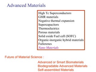
- 1. Advanced Materials High Tc Superconductors GMR materials Negative thermal expansion Supercapacitors Thermoelectrics Porous materials Solid oxide Fuel cell (SOFC) Organic-inorganic hybrid materials Fullerenes Nano Materials Advanced or Smart Biomaterials Biodegradable Advanced Materials Self-assembled Materials Future of Material Science :
- 2. Nanostructured materials for technologies in 2015 and beyond Professor A K Ganguli Department of Chemistry Indian Institute of Technology Delhi New Delhi 110016 [email_address] March 9, Bangalore, EmTech India 2010
- 3. E.U USA Japan China Rest of world Global Government Funding 12000 million dollars 2600 million dollars N A N O T E C H N O L O G Y
- 4. Large industry currently supports about half of the R&D in U.S_ $2 billion per yr. CHINA Russia <1% to 23% 2004 2009 3% to 10% INDIA less than 1 % J. Nanoparticle Res. (2010) Global Nanotech Funds
- 7. Variety of nanomaterials NaNbO 3 Electroceramics Catalysts magnetics, catalysts Photocatalysts Toxin traps Batteries BaTiO 3 MnC 2 O 4 MnO, Mn 2 O 3 Mn 3 O 4 CdS @ TiO 2 [email_address] 2 Co Ba 2 TiO 4 FeC 2 O 4 Fe 2 O 3 , Fe 3 O 4 CdS @ SiO 2 Cu SrTiO 3 CoC 2 O 4 CoO, Co 3 O 4 NiS @ TiO 2 Ni Sr 2 TiO 4 NiC 2 O 4 NiO NiS @ SiO 2 Cu-Ni PbTiO 3 CuC 2 O 4 CuO [email_address] 2 Co-Ni BaZrO 3 ZnC 2 O 4 ZnO [email_address] 2 Co-Cu SrZrO 3 CdC 2 O 4 SnO 2 GMR materials Magnetic recording Mn-Ni PbZrO 3 Ce 2 (C 2 O 4 ) 3 ZrO 2 LaMnO 3 Hard coatings Fe 2 (C 2 H 4 C 2 O 4 ) 3 CeO 2 La .67 Sr .33 MnO 3 LaB 6 NaTaO 3 CoC 2 H 4 C 2 O 4 La .67 Ca .33 MnO 3 NbB 2 SrTa 2 O 6 CuC 2 H 4 C 2 O 4 CrB 2
- 9. Controlling shape CTAB/1-butanol/Isooctane TX-100/1-hexanol/cyclohexane Tergitol/1-octanol/cyclohexane NiC 2 O 4 .2H 2 O Ganguli et al, J. Phys. Chem. C 2008, 112, 12610–12615. NiO 20 nm 10 nm 25 nm
- 10. Silica nanoparticles on copper succinate nanorods silica nanoparticles coated with aminoacid. By reverse micelles Commercially available NANO - SiO 2 SiO 2 Aparna Ganguly et al IITD 100nm 100 nm
- 11. Silica particles (40 nm) : Aparna et al, Journal of ClusterScience (2009) 50 nm Porous silica (200 nm) Pores : 5 nm 550 m 2 /g 120 m 2 /g
- 14. Formation and shape evolution of nano-heterostructures ( metal – carbon) Chem. Mater. , 2007 , 19 (26), 6376-6378
- 15. Nanowire welding using DNA T. Mallouk Penn. State Univ. SH-DNA Au Complementary DNA strands on two wires
- 16. Quantum Dot Solar Cells Complex functionalized Nanostructures
- 17. Carbon Nanotubes, (S. Iijima, 1991 ) Single nanotube ..transistor (1998, IBM) may replace silicon Field effect transistors produced (Stanford/Cornell/Purdue) Improved Carbon –based FET, IBM,2002 outperforms Si-based transistors, twice current carrying capacity World’s smallest computer logic circuit , IBM 2001
- 18. CNT Applications Sensors, Bio, NEMS • Electronics • Challenges Challenges • Control of diameter, chirality • Doping, contacts • Novel architectures (not CMOS based!) • Development of inexpensive Manufacturing processes • Controlled growth • Functionalization with probe molecules, robustness • Integration, signal processing • Fabrication techniques
- 19. Cost contributions from each process step (a–c) and fixed and variable cost contributions (d–f) for arc, CVD, and HiPco processes Needs to be reduced Needs to be reduced Cost of synthesis Cost of Labour
- 24. Core – shell nanostructures Core Shell Methyl Orange Toxin Traps Ganguli et al (2009) SiO 2 Metal oxide Hollow shell Hollow shells 002 200 Ag crystalline TiO 2 amorphous 5 nm
- 25. ZnO @ CdS Core Shell Nanorods Photocurrent Assembly of core-shell on a substrate CdS quantum dot sensitized solar cell based on a mesoporous TiO2 film : 1.24% J. Phys. Chem. C 2009, IITD (2010)
- 26. Nanoelectronics Smaller size of electronic components resistors, transistors, capacitors, • Processors with increasing efficiency of computer by 10 6 • Higher transmission frequencies and more efficient utilization of optical spectrum to provide higher bandwidth • Small mass storage devices: multi-tera bit levels
- 27. Dielectric Nanoparticles Nanosized dielectric oxides (40-50 nm) will allow thin dielectric layers Less dissipation factor Need for miniaturization of device components 1990 limit (12 µm) current feature size (chip) ~ 140 nm; by 2014 ~ 50-70 nm MLCC ( Multilayer ceramic capacitor) For power line stabilization in the packaging of Si –based IC’s ( Pd /Ag)
- 28. + Micron-sized Nanosized grains Heat (Sinter) Schematic Microstructure Lower M. Pt. Electroceramics : Nanocomposites “ ( n µ) - Composites” Barium titanium oxide Enhancing the dielectric properties using nano-dopants
- 29. n μ -composite of BaTiO 3 Sintered disk Dielectric constant is maximum at 1 wt% composition oscillatory nature V. Shanker, T. Ahmad, H. Ip and A. K. Ganguli. J. Mater. Res., 21, 816 (2006) At ~25 o C Bulk BaTiO 3 1 wt% BaTiO 3
- 30. Nanomaterials in Medical applications
- 31. Biosensor
- 34. • More efficient catalytic converters • Thermal barrier and wear resistant coatings • Battery, fuel cell technology • Improved displays • Wear-resistant tires • High temperature sensors for ‘under the hood’; novel sensors for “all-electric” vehicles • High strength, light weight composites for increasing fuel efficiency Scope of Nanomaterials for transportation Carbon –based fibres, polymer-metal nanocomposites
- 38. GRAPHENE realized in 2004 (Novoselov, Science 306 , 2004) Predicted in 1947 Intrinsic graphene is a semi-metal or zero-gap semiconductor remarkably high electron mobility at room temperature pure graphene is transparent ideal material for spintronics light-emitting diodes (LEDs) , improved solar cells Material of the Future Large scale synthesis of pure Graphene : Challenge
- 40. Cost of some nanomaterials 3360 50g 15 nm 99.5 Silica 3696 50g 10 nm 99.5 Silica 2399 25g 99.5 Rutile 4982 50g 5 nm 99.7 Anatase 2620 25g 25-70 nm 99.9 Mixture of Anatase and rutile 13860 250 mg 1.3-2.0 nm * 50 μ m 50 (CVD) CNT (doublewalled) 13860 250 mg 1.1 nm * 0.5-100 μ m 50 (CVD) CNT (single walled) 5290 250 mg 1.2-1.5 nm * 2-5 μ m 50 (Arc method) CNT (single walled) 6540 25g 10-20 nm 99.7 CaZrO 3 5395 25g 60-100 nm 99.9 CaTiO 3 3638 25g 30-50 nm 99+ BaTiO 3 Cost (Rs) Quantity Avg size % purity Compund
- 41. Molecules are important ( Molecular electronics) 30 nm Bottom –up approach The future : self assembled circuits with molecular components Molecular machines motor proteins
- 42. Synthetic molecular motors Chemically driven rotary molecular motors first example : Kelly and co-workers in 1999 rotation takes place in five steps amine group present on the triptycene moiety is converted to an isocyanate group Light-driven rotary molecular motors Photochromic molecular switches
- 45. bistable [2]rotaxane used as storage unit in the crossbar memory (molecular switch) Green et. Al. Nature, (2007) circumrotation translation Si nanowire Pt/Ti nanowire TTF TTF + Balzani et al , J. Org Chem (2000) Molecular shuttle
- 48. With electricity : sizeable voltage is needed and the process is not very efficient catalysts : a smaller voltage Production of oxygen and hydrogen gas powered by solar photovoltaic cells Mimic a green Leaf : A Photoelectrochemical cell can help to split water Mostly with UV light low conversion efficiencies and relatively high cost. . No material capable of catalyzing reaction with visible light and a QE larger than 10% Store H 2 , Couple with O 2 in a Fuel Cell Energy ( in absence of Light)
- 50. c 111 Rod shaped copper particles cube shaped copper particles spherical shaped copper particles Hydrogen evolution reaction Ganguli et al 2010 Shape-dependent Copper nanostructures as electrocatalysts 20 nm
- 53. Most complex molecules are synthesized atom by atom chemically Self-organization leads to complex supramolecular entities Brain -----Most Complex computer , made of molecules , run by molecules/ions Life is possible because of chemical information processing Influenced by some lectures of Jean Marie Pierre Lehn , N. L. in Chemistry, 1987 Some Thoughts The Key is to use chemistry ( solution – based processes) together with the knowledge of biologically relevant molecules and processes
- 55. Department of Science & Technolgy, Govt. of India Nanomission, Physical Chemistry & ( IITD-EPFL) projects Ministry of Human Res. & Dev., Govt. of India Council of Scientific & Industrial Research, Govt. of India