Digital system design practical file
•
8 gefällt mir•6,562 views

Full details of the various practicals including circuit diagrams and truth tables.

Empfohlen
Weitere ähnliche Inhalte
Was ist angesagt?
Was ist angesagt? (20)
Andere mochten auch
Andere mochten auch (19)
Ähnlich wie Digital system design practical file
Ähnlich wie Digital system design practical file (20)
Mehr von Archita Misra
Mehr von Archita Misra (6)
Kürzlich hochgeladen
Kürzlich hochgeladen (20)
Digital system design practical file
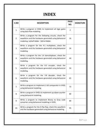
- 1. 1 | P a g e INDEX S.NO DESCRIPTION PAGE 1. Write a program in VHDL to implement all logic gates using data flow modeling. 2 2. Write a program for the following circuits, check the waveform and the hardware generated using behavioral modeling: (a)Half Adder (b)Full Adder 16 3. Write a program for the 4:1 multiplexer, check the waveform and the hardware generated using behavioral modeling. 34 4. Write a program for the 1:4 demultiplexer, check the waveform and the hardware generated using behavioral modeling. 44 5. Write a program for the 8:3 encoder, check the waveform and the hardware generated using behavioral modeling. 54 6. Write a program for the 3:8 decoder, check the waveform and the hardware generated using behavioral modeling. 65 7. Write a program to implement 1-bit comparator in VHDL using behavioral modeling. 73 8. Write a program in VHDL to implement up-down counter using behavioral modeling. 80 9. Write a program to implement Binary to Gray code converter using behavioral modeling in VHDL 89 10. Write a program for the D flip-flop, check the waveform and the hardware generated using behavioral modeling. 95 SIGNATURE NO.
- 2. 2 | P a g e Program 1 Aim: Write a program in VHDL to implement all logic gates using data flow modeling. Apparatus: Tool used: Xilinx 8.2i PC specification: 1GB RAM, 320GB hard disk Theory: AND gate: The AND gate is an electronic circuit that gives a high output (1) only if all its inputs are high. A dot (.) is used to show the AND operation i.e. A.B. Bear in mind that this dot is sometimes omitted i.e. AB. OR gate: The OR gate is an electronic circuit that gives a high output (1) if one or more of its inputs are high. A plus (+) is used to show the OR operation. NOT gate: The NOT gate is an electronic circuit that produces an inverted version of the input at its output. It is also known as an inverter. If the input variable is A, the inverted output is known as NOT A. This is also shown as A', or A with a bar over the top, as shown at the outputs. The diagrams below show two ways that the NAND logic gate can be configured to produce a NOT gate. It can also be done using NOR logic gates in the same way. NAND gate: This is a NOT-AND gate which is equal to an AND gate followed by a NOT gate. The outputs of all NAND gates are high if any of the inputs are low. The symbol is an AND gate with a small circle on the output. The small circle represents inversion. NOR gate: This is a NOT-OR gate which is equal to an OR gate followed by a NOT gate. The outputs of all NOR gates are low if any of the inputs are high. The symbol is an OR gate with a small circle on the output. The small circle represents inversion. XOR gate: The 'Exclusive-OR' gate is a circuit which will give a high output if either, but not both, of its two inputs are high. An encircled plus sign ( ) is used to show the EOR operation. XNOR gate: The 'Exclusive-NOR' gate circuit does the opposite to the EOR gate. It will give a low output if either, but not both, of its two inputs are high. The symbol is an EXOR gate with a small circle on the output. The small circle represents inversion.
- 3. 3 | P a g e VHDL code for implementing logic gates using data flow modeling: library IEEE; use IEEE.STD_LOGIC_1164.ALL; use IEEE.STD_LOGIC_ARITH.ALL; use IEEE.STD_LOGIC_UNSIGNED.ALL; ---- Uncomment the following library declaration if instantiating ---- any Xilinx primitives in this code. --library UNISIM; --use UNISIM.VComponents.all; entity gates_new is Port ( a : in STD_LOGIC; b : in STD_LOGIC; y1 : out STD_LOGIC; y2 : out STD_LOGIC; y3 : out STD_LOGIC; y4 : out STD_LOGIC; y5 : out STD_LOGIC; y6 : out STD_LOGIC; y7 : out STD_LOGIC); end gates_new; architecture Behavioral of gates_new is begin y1<=a and b;
- 4. 4 | P a g e y2<=a or b; y3<=not a; y4<=a nand b; y5<=a nor b; y6<=a xor b; y7<=a xnor b; end Behavioral; RTL schematic diagram for all logic gates:
- 5. 5 | P a g e
- 6. 6 | P a g e Technology schematic diagram for all logic gates: AND gate: Truth table:
- 7. 7 | P a g e OR gate: Truth table: NAND gate: Truth table:
- 8. 8 | P a g e NOR gate: Truth table: XOR gate: Truth table:
- 9. 9 | P a g e XNOR gate: Truth table: Test Bench for implementing all logic gates using data flow modeling: LIBRARY ieee; USE ieee.std_logic_1164.ALL; USE ieee.std_logic_unsigned.all; USE ieee.numeric_std.ALL; ENTITY gates_new_tb_vhd IS END gates_new_tb_vhd; ARCHITECTURE behavior OF gates_new_tb_vhd IS -- Component Declaration for the Unit Under Test (UUT) COMPONENT gates_new PORT(
- 10. 10 | P a g e a : IN std_logic; b : IN std_logic; y1 : OUT std_logic; y2 : OUT std_logic; y3 : OUT std_logic; y4 : OUT std_logic; y5 : OUT std_logic; y6 : OUT std_logic; y7 : OUT std_logic ); END COMPONENT; --Inputs SIGNAL a : std_logic := '0'; SIGNAL b : std_logic := '0'; --Outputs SIGNAL y1 : std_logic; SIGNAL y2 : std_logic; SIGNAL y3 : std_logic; SIGNAL y4 : std_logic; SIGNAL y5 : std_logic; SIGNAL y6 : std_logic; SIGNAL y7 : std_logic; BEGIN
- 11. 11 | P a g e -- Instantiate the Unit Under Test (UUT) uut: gates_new PORT MAP( a => a, b => b, y1 => y1, y2 => y2, y3 => y3, y4 => y4, y5 => y5, y6 => y6, y7 => y7 ); tb : PROCESS BEGIN -- Place stimulus here a<='0','1' after 100ns,'0' after 200ns; b<='0','1' after 50ns,'0' after 100ns,'1' after 150ns; wait; -- will wait forever END PROCESS; END;
- 12. 12 | P a g e Simulation waveform:
- 13. 13 | P a g e Program 2 Aim: To write a program for the following circuits, check the waveform and the hardware generated using behavioral modeling. (a)Half adder (b)Full adder Apparatus: Tool used: Xilinx 8.2i PC specification: 1GB RAM, 320GB hard disk (A) HALF ADDER Theory: The half adder adds two single binary digits A and B. It has two outputs, sum (S) and carry (C). The carry signal represents an overflow into the next digit of a multi-digit addition. The value of the sum is 2C + S. The simplest half-adder design, incorporates an XOR gate for S and an AND gate for C. With the addition of an OR gate to combine their carry outputs, two half adders can be combined to make a full adder.
- 14. 14 | P a g e VHDL code for implementing half adder using behavioral modeling: library IEEE; use IEEE.STD_LOGIC_1164.ALL; use IEEE.STD_LOGIC_ARITH.ALL; use IEEE.STD_LOGIC_UNSIGNED.ALL; ---- Uncomment the following library declaration if instantiating ---- any Xilinx primitives in this code. --library UNISIM; --use UNISIM.VComponents.all; entity half_adder is Port ( a : in STD_LOGIC; b : in STD_LOGIC; sum : out STD_LOGIC; carry : out STD_LOGIC); end half_adder; architecture Behavioral of half_adder is begin sum<=a xor b; carry<=a and b; end Behavioral;
- 15. 15 | P a g e RTL Schematic Diagram for implementing half adder:
- 16. 16 | P a g e Technology Schematic Diagram for implementing half adder: For SUM: Truth table:
- 17. 17 | P a g e For CARRY: Truth table: Test Bench for implementing half adder: LIBRARY ieee; USE ieee.std_logic_1164.ALL; USE ieee.std_logic_unsigned.all; USE ieee.numeric_std.ALL; ENTITY half_adder_tb_vhd IS END half_adder_tb_vhd;
- 18. 18 | P a g e ARCHITECTURE behavior OF half_adder_tb_vhd IS -- Component Declaration for the Unit Under Test (UUT) COMPONENT half_adder PORT( a : IN std_logic; b : IN std_logic; sum : OUT std_logic; carry : OUT std_logic ); END COMPONENT; --Inputs SIGNAL a : std_logic := '0'; SIGNAL b : std_logic := '0'; --Outputs SIGNAL sum : std_logic; SIGNAL carry : std_logic; BEGIN -- Instantiate the Unit Under Test (UUT) uut: half_adder PORT MAP( a => a, b => b,
- 19. 19 | P a g e sum => sum, carry => carry ); tb : PROCESS BEGIN a<='0','1' after 100ns,'0' after 200ns; b<='0','1' after 50ns,'0' after 100ns,'1' after 150ns; wait; -- will wait forever END PROCESS; END; Simulation waveform for half adder:
- 20. 20 | P a g e (B) FULL ADDER Theory: A full adder adds binary numbers and accounts for values carried in as well as out. A one-bit full adder adds three one-bit numbers, often written as A, B, and Cin; A and B are the operands, and Cin is a bit carried in from the next less significant stage.[2] The full-adder is usually a component in a cascade of adders, which add 8, 16, 32, etc. binary numbers. The circuit produces a two-bit output, output carry and sum typically represented by the signals Cout and S, where . VHDL code for implementing full adder using behavioral modeling: library IEEE; use IEEE.STD_LOGIC_1164.ALL; use IEEE.STD_LOGIC_ARITH.ALL; use IEEE.STD_LOGIC_UNSIGNED.ALL; ---- Uncomment the following library declaration if instantiating ---- any Xilinx primitives in this code. --library UNISIM; --use UNISIM.VComponents.all; entity full_adder is Port ( a : in STD_LOGIC; b : in STD_LOGIC; cin : in STD_LOGIC; sum : out STD_LOGIC; carry : out STD_LOGIC); end full_adder; architecture Behavioral of full_adder is
- 21. 21 | P a g e begin sum<=a xor b xor cin; carry<=(a and b)or(a and cin)or(b and cin); end Behavioral; RTL Schematic Diagram for implementing full adder:
- 22. 22 | P a g e Technology Schematic Diagram for implementing full adder: For SUM: Truth table:
- 23. 23 | P a g e For CARRY: Truth table: Test Bench for implementing full adder: LIBRARY ieee; USE ieee.std_logic_1164.ALL; USE ieee.std_logic_unsigned.all; USE ieee.numeric_std.ALL; ENTITY full_adder_tb_vhd IS END full_adder_tb_vhd;
- 24. 24 | P a g e ARCHITECTURE behavior OF full_adder_tb_vhd IS -- Component Declaration for the Unit Under Test (UUT) COMPONENT full_adder PORT( a : IN std_logic; b : IN std_logic; cin : IN std_logic; sum : OUT std_logic; carry : OUT std_logic ); END COMPONENT; --Inputs SIGNAL a : std_logic := '0'; SIGNAL b : std_logic := '0'; SIGNAL cin : std_logic := '0'; --Outputs SIGNAL sum : std_logic; SIGNAL carry : std_logic; BEGIN -- Instantiate the Unit Under Test (UUT) uut: full_adder PORT MAP( a => a,
- 25. 25 | P a g e b => b, cin => cin, sum => sum, carry => carry ); tb : PROCESS BEGIN -- Wait 100 ns for global reset to finish -- Place stimulus here a<='0','1' after 100ns,'0' after 200ns; b<='0','1' after 50ns,'0' after 100ns,'1' after 150ns; cin<='0','1' after 50ns,'0' after 150ns,'1' after 200ns; wait; -- will wait forever END PROCESS; END; Simulation Waveform for Full Adder:
- 26. 26 | P a g e Program 3 Aim: To write a program for the 4:1 multiplexer, check the waveform and the hardware generated using behavioral modeling. Apparatus: Tool used: Xilinx 8.2i PC specification: 1GB RAM, 320GB hard disk Theory: In electronics, a multiplexer (or mux) is a device that selects one of several analog or digital input signals and forwards the selected input into a single line. A multiplexer of 2n inputs has n select lines, which are used to select which input line to send to the output. Multiplexers are mainly used to increase the amount of data that can be sent over the network within a certain amount of time and bandwidth. A multiplexer is also called a data selector. An electronic multiplexer makes it possible for several signals to share one device or resource, for example one A/D converter or one communication line, instead of having one device per input signal. 4:1 multiplexer
- 27. 27 | P a g e VHDL code for implementing 4:1 multiplexer using behavioral modeling: library IEEE; use IEEE.STD_LOGIC_1164.ALL; use IEEE.STD_LOGIC_ARITH.ALL; use IEEE.STD_LOGIC_UNSIGNED.ALL; ---- Uncomment the following library declaration if instantiating ---- any Xilinx primitives in this code. --library UNISIM; --use UNISIM.VComponents.all; entity mux4to1 is Port ( i0 : in STD_LOGIC; i1 : in STD_LOGIC; i2 : in STD_LOGIC; i3 : in STD_LOGIC; s0 : in STD_LOGIC; s1 : in STD_LOGIC; y : out STD_LOGIC); end mux4to1; architecture Behavioral of mux4to1 is begin process(i0,i1,i2,i3,s0,s1)
- 28. 28 | P a g e begin if(s1='0' and s0='0') then y<=i0; elsif(s1='0' and s0='1') then y<=i1; elsif(s1='1' and s0='0') then y<=i2; else y<=i3; end if; end process; end Behavioral; RTL Schematic Diagram for implementing 4:1 multiplexer:
- 29. 29 | P a g e Technology Schematic Diagram for implementing 4:1 multiplexer:
- 30. 30 | P a g e Test bench for 4:1 multiplexer: HDL Test Bench LIBRARY ieee; USE ieee.std_logic_1164.ALL; USE ieee.std_logic_unsigned.all; USE ieee.numeric_std.ALL; ENTITY pgm3_tb_vhd IS END pgm3_tb_vhd; ARCHITECTURE behavior OF pgm3_tb_vhd IS -- Component Declaration for the Unit Under Test (UUT)
- 31. 31 | P a g e COMPONENT pgm3 PORT( i0 : IN std_logic; i1 : IN std_logic; i2 : IN std_logic; i3 : IN std_logic; S0 : IN std_logic; S1 : IN std_logic; Y : OUT std_logic ); END COMPONENT; --Inputs SIGNAL i0 : std_logic := '0'; SIGNAL i1 : std_logic := '0'; SIGNAL i2 : std_logic := '0'; SIGNAL i3 : std_logic := '0'; SIGNAL S0 : std_logic := '0'; SIGNAL S1 : std_logic := '0'; --Outputs SIGNAL Y : std_logic; BEGIN -- Instantiate the Unit Under Test (UUT) uut: pgm3 PORT MAP( i0 => i0, i1 => i1, i2 => i2, i3 => i3, S0 => S0, S1 => S1, Y => Y
- 32. 32 | P a g e ); tb : PROCESS BEGIN -- Place stimulus here i0<='0','1' after 50ns, '0' after 100ns; i1<='0','1' after 100ns, '0' after 150ns, '1' after 200ns; i2<='0','1' after 50ns, '0' after 100ns; i3<='0','1' after 50ns, '0' after 100ns, '1' after 200ns; S0<='0','1' after 150ns, '0' after 200ns; S1<='0','1' after 50ns, '0' after 100ns; wait; -- will wait forever END PROCESS; END; Simulation waveform for 4:1 multiplexer:
- 33. 33 | P a g e Program 4 Aim: To write a program for the 1:4 demultiplexer, check the waveform and the hardware generated using behavioral modeling. Apparatus: Tool used: Xilinx 8.2i PC specification: 1GB RAM, 320GB hard disk Theory: A demultiplexer (or demux) is a device taking a single input signal and selecting one of many data-output-lines, which is connected to the single input. A multiplexer is often used with a complementary demultiplexer on the receiving end. Demultiplexers take one data input and a number of selection inputs, and they have several outputs. They forward the data input to one of the outputs depending on the values of the selection inputs. Demultiplexers are sometimes convenient for designing general purpose logic, because if the demultiplexer's input is always true, the demultiplexer acts as a decoder. This means that any function of the selection bits can be constructed by logically OR-ing the correct set of outputs. 1:4 demultiplexer
- 34. 34 | P a g e VHDL code for implementing 1:4 demultiplexer using behavioral modeling: library IEEE; use IEEE.STD_LOGIC_1164.ALL; use IEEE.STD_LOGIC_ARITH.ALL; use IEEE.STD_LOGIC_UNSIGNED.ALL; ---- Uncomment the following library declaration if instantiating ---- any Xilinx primitives in this code. --library UNISIM; --use UNISIM.VComponents.all; entity demux is Port ( Y : in STD_LOGIC; S0 : in STD_LOGIC; S1 : in STD_LOGIC; I0 : out STD_LOGIC; I1 : out STD_LOGIC; I2 : out STD_LOGIC; I3 : out STD_LOGIC); end demux; architecture Behavioral of demux is begin process(Y,S1,S0) begin if(S1='0' and S0='0') then
- 35. 35 | P a g e I0<=Y; Elsif(S1='0' and S0='1') then I1<=Y; Elsif(S1='1' and S0='0') then I2<=Y; Elsif(S1='1' and S0='1') then I3<=Y; End if; End process; end Behavioral; RTL Schematic Diagram for implementing 1:4 demultiplexer:
- 36. 36 | P a g e Technology Schematic Diagram for implementing 1:4 demultiplexer: Truth Table:
- 37. 37 | P a g e
- 38. 38 | P a g e VHDL Test Bench using for 1:4 demultiplexer: VHDL TEST BENCH LIBRARY ieee; USE ieee.std_logic_1164.ALL; USE ieee.std_logic_unsigned.all; USE ieee.numeric_std.ALL; ENTITY demux_tb_vhd IS END demux_tb_vhd; ARCHITECTURE behavior OF demux_tb_vhd IS -- Component Declaration for the Unit Under Test (UUT) COMPONENT demux PORT( Y : IN std_logic; S0 : IN std_logic; S1 : IN std_logic; I0 : OUT std_logic; I1 : OUT std_logic; I2 : OUT std_logic; I3 : OUT std_logic ); END COMPONENT; --Inputs SIGNAL Y : std_logic := '0'; SIGNAL S0 : std_logic := '0'; SIGNAL S1 : std_logic := '0'; --Outputs SIGNAL I0 : std_logic; SIGNAL I1 : std_logic; SIGNAL I2 : std_logic; SIGNAL I3 : std_logic; BEGIN -- Instantiate the Unit Under Test (UUT) uut: demux PORT MAP(
- 39. 39 | P a g e Y => Y, S0 => S0, S1 => S1, I0 => I0, I1 => I1, I2 => I2, I3 => I3 ); tb : PROCESS BEGIN -- Place stimulus here S0<='0','1' after 150ns, '0' after 200ns; S1<='0','1' after 50ns, '0' after 100ns, '1' after 200ns; wait; -- will wait forever END PROCESS; END; Simulation Waveform for 1:4 demultiplexer :
- 40. 40 | P a g e Program 5 Aim: To write a program for the 8:3 encoder, check the waveform and the hardware generated using behavioral modeling. Apparatus: Tool used: Xilinx 8.2i PC specification: 1GB RAM, 320GB hard disk Theory: An encoder is a device, circuit, transducer, software program, algorithm or person that converts information from one format or code to another. The purpose of encoder is standardization, speed, secrecy, security, or saving space by shrinking size. Encoders are combinational logic circuits and they are exactly opposite of decoders. They accept one or more inputs and generate a multibit output code. Encoders perform exactly reverse operation than decoder. An encoder has M input and N output lines. Out of M input lines only one is activated at a time and produces equivalent code on output N lines. If a device output code has fewer bits than the input code has, the device is usually called an encoder. Truth table for 8:3 encoder:-
- 41. 41 | P a g e VHDL code for implementing 8:3 encoder using behavioral modeling: library IEEE; use IEEE.STD_LOGIC_1164.ALL; use IEEE.STD_LOGIC_ARITH.ALL; use IEEE.STD_LOGIC_UNSIGNED.ALL; ---- Uncomment the following library declaration if instantiating ---- any Xilinx primitives in this code. --library UNISIM; --use UNISIM.VComponents.all; entity encod8to3 is Port ( i : in STD_LOGIC_VECTOR (7 downto 0); y : out STD_LOGIC_VECTOR (2 downto 0); enable : in STD_LOGIC); end encod8to3; architecture Behavioral of encod8to3 is begin process(i,enable) begin if(enable='0') then y<="000"; else case i is
- 42. 42 | P a g e when "00000001" => y <="000"; when "00000010" => y <="001"; when "00000100" => y <="010"; when "00001000" => y <="011"; when "00010000" => y <="100"; when "00100000" => y <="101"; when "01000000" => y <="110"; when "10000000" => y <="111"; when others => y <="000"; end case; end if; end process; end Behavioral;
- 43. 43 | P a g e RTL Schematic Diagram for implementing 8:3 encoder:
- 44. 44 | P a g e
- 45. 45 | P a g e
- 46. 46 | P a g e Technology Schematic Diagram for implementing 8:3 encoder:
- 47. 47 | P a g e Test bench for 8:3 encoder: LIBRARY ieee; USE ieee.std_logic_1164.ALL; USE ieee.std_logic_unsigned.all; USE ieee.numeric_std.ALL; ENTITY encd_tb_vhd IS END encd_tb_vhd; ARCHITECTURE behavior OF encd_tb_vhd IS
- 48. 48 | P a g e -- Component Declaration for the Unit Under Test (UUT) COMPONENT encod8to3 PORT( i : IN std_logic_vector(7 downto 0); enable : IN std_logic; y : OUT std_logic_vector(2 downto 0) ); END COMPONENT; --Inputs SIGNAL enable : std_logic := '0'; SIGNAL i : std_logic_vector(7 downto 0) := (others=>'0'); --Outputs SIGNAL y : std_logic_vector(2 downto 0); BEGIN -- Instantiate the Unit Under Test (UUT) uut: encod8to3 PORT MAP( i => i, y => y, enable => enable );
- 49. 49 | P a g e tb : PROCESS BEGIN enable<='1'; i<="00000001","00000010" after 10ns,"00000100" after 20ns,"00001000" after 30ns, "00010000" after 40ns,"00100000" after 50ns,"01000000" after 60ns,"10000000" after 70ns; wait; -- will wait forever END PROCESS; END; Simulation waveform for 8:3 encoder :
- 50. 50 | P a g e Program 6 Aim: To write a program for the 3:8 decoder, check the waveform and the hardware generated using behavioral modeling. Apparatus: Tool used: Xilinx 8.2i PC specification: 1GB RAM, 320GB hard disk Theory: In digital electronics, a decoder can take the form of a multiple-input, multiple-output logic circuit that converts coded inputs into coded outputs, where the input and output codes are different e.g. n-to-2n , binary-coded decimal decoders. Decoding is necessary in applications such as data multiplexing, 7 segment display and memory address decoding. 3:8 decoder uses all AND gates, and therefore, the outputs are active- high. For active- low outputs, NAND gates are used. It has 3 input lines and 8 output lines. It is also called as binary to octal decoder it takes a 3-bit binary input code and activates one of the 8(octal) outputs corresponding to that code. The truth table is as follows: Truth Table of 3:8 decoder
- 51. 51 | P a g e VHDL code for implementing 3:8 decoder using behavioral modeling: library IEEE; use IEEE.STD_LOGIC_1164.ALL; use IEEE.STD_LOGIC_ARITH.ALL; use IEEE.STD_LOGIC_UNSIGNED.ALL; ---- Uncomment the following library declaration if instantiating ---- any Xilinx primitives in this code. --library UNISIM; --use UNISIM.VComponents.all; entity dec3to8 is Port ( i : in STD_LOGIC_VECTOR (2 downto 0); o : out STD_LOGIC_VECTOR (7 downto 0); enable : in STD_LOGIC); end dec3to8; architecture Behavioral of dec3to8 is begin process(i,enable) begin if(enable='0') then o<="00000000"; else case i is
- 52. 52 | P a g e when "000" => o <="00000001"; when "001"=> o <= "00000010"; when "010"=> o <= "00000100"; when "011"=> o <= "00001000"; when "100"=> o <= "00010000"; when "101"=> o <= "00100000"; when "110"=> o <= "01000000"; when "111"=> o<= "10000000"; when others => o <="00000000"; end case; end if; end process; end Behavioral; RTL Schematic Diagram for implementing 3:8 decoder:
- 53. 53 | P a g e Technology Schematic Diagram for implementing 3:8 decoder:
- 54. 54 | P a g e VHDL Test Bench using for 3:8 decoder: LIBRARY ieee; USE ieee.std_logic_1164.ALL; USE ieee.std_logic_unsigned.all; USE ieee.numeric_std.ALL; ENTITY dec3to8_tb_vhd IS END dec3to8_tb_vhd; ARCHITECTURE behavior OF dec3to8_tb_vhd IS -- Component Declaration for the Unit Under Test (UUT)
- 55. 55 | P a g e COMPONENT dec3to8 PORT( i : IN std_logic_vector(2 downto 0); enable : IN std_logic; o : OUT std_logic_vector(7 downto 0) ); END COMPONENT; --Inputs SIGNAL enable : std_logic := '0'; SIGNAL i : std_logic_vector(2 downto 0) := (others=>'0'); --Outputs SIGNAL o : std_logic_vector(7 downto 0); BEGIN -- Instantiate the Unit Under Test (UUT) uut: dec3to8 PORT MAP( i => i, o => o, enable => enable ); tb : PROCESS
- 56. 56 | P a g e BEGIN enable<='1'; i<="000","001" after 10ns, "010" after 20ns,"011" after 30ns,"100" after 40ns,"101" after 50ns,"110" after 60ns,"111" after 70ns; -- Place stimulus here wait; -- will wait forever END PROCESS; END; Simulation Waveform for 3:8 decoder :
- 57. 57 | P a g e Program 7 Aim: Write a program to implement 1-bit comparator in VHDL using behavioral modeling. Apparatus: Tool used: Xilinx 8.2i PC specification: 1GB RAM, 320GB hard disk Theory: A digital comparator or magnitude comparator is a hardware electronic device that takes two numbers as input in binary form and determines whether one number is greater than, less than or equal to the other number. Comparators are used in central processing units (CPUs) and microcontrollers (MCUs). The operation of a single bit digital comparator can be expressed as a truth table:
- 58. 58 | P a g e VHDL code for implementing 1-bit comparator using behavioral modeling: library IEEE; use IEEE.STD_LOGIC_1164.ALL; use IEEE.STD_LOGIC_ARITH.ALL; use IEEE.STD_LOGIC_UNSIGNED.ALL; ---- Uncomment the following library declaration if instantiating ---- any Xilinx primitives in this code. --library UNISIM; --use UNISIM.VComponents.all; entity com is Port ( a : in STD_LOGIC; b : in STD_LOGIC; agb : out STD_LOGIC; aeb : out STD_LOGIC; alb : out STD_LOGIC); end com; architecture Behavioral of com is begin process(a,b) begin if(a>b)then agb<='1'; aeb<='0'; alb<='0'; elsif(a=b) then agb<='0'; aeb<='1'; alb<='0'; elsif(a<b) then agb<='0'; aeb<='0'; alb<='1'; end if; end process; end Behavioral;
- 59. 59 | P a g e RTL schematic diagram for 1-bit comparator:
- 60. 60 | P a g e Technology schematic diagram for 1-bit comparator:
- 61. 61 | P a g e Truth tables:
- 62. 62 | P a g e Test Bench for implementing 1-bit comparator using behavioral modeling: LIBRARY ieee; USE ieee.std_logic_1164.ALL; USE ieee.std_logic_unsigned.all; USE ieee.numeric_std.ALL; ENTITY com_tb_vhd IS END com_tb_vhd; ARCHITECTURE behavior OF com_tb_vhd IS -- Component Declaration for the Unit Under Test (UUT) COMPONENT com PORT( a : IN std_logic; b : IN std_logic; agb : OUT std_logic; aeb : OUT std_logic; alb : OUT std_logic ); END COMPONENT; --Inputs SIGNAL a : std_logic := '0'; SIGNAL b : std_logic := '0'; --Outputs SIGNAL agb : std_logic; SIGNAL aeb : std_logic; SIGNAL alb : std_logic; BEGIN -- Instantiate the Unit Under Test (UUT) uut: com PORT MAP( a => a, b => b, agb => agb, aeb => aeb,
- 63. 63 | P a g e alb => alb ); tb : PROCESS BEGIN -- Place stimulus here a<='0','1' after 20ns,'0' after 100ns,'1' after 150ns; b<='0','1' after 20ns,'0' after 80ns,'1' after 120ns; wait; -- will wait forever END PROCESS; END; Simulation Waveform for 1-bit comparator :
- 64. 64 | P a g e Program 8 Aim: Write a program in VHDL to implement up-down counter using behavioral modeling. Apparatus: Tool used: Xilinx 8.2i PC specification: 1GB RAM, 320GB hard disk Theory: The similarities between the implementation of a binary up counter and a binary down counter leads to the possibility of a binary up/down counter, which is a binary up counter and a binary down counter combined into one. Since the difference is only in which output of the flip- flop to use, the normal output or the inverted one, we use two AND gates for each flip-flop to "choose" which of the output to use. From the diagram, we can see that COUNT-UP and COUNT-DOWN are used as control inputs to determine whether the normal flip-flop outputs or the inverted ones are fed into the J-K inputs of the following flip-flops. If neither is at logic level 1, the counter doesn't count and if both are at logic level 1, all the bits of the counter toggle at every clock pulse. The OR gate allows either of the two outputs which have been enabled to be fed into the next flip-flop. As with the binary up and binary down counter, the speed up techniques apply. 3-Bit Synchronous Up-Down Counter
- 65. 65 | P a g e VHDL code for implementing up-down counter using behavioral modeling: library IEEE; use IEEE.STD_LOGIC_1164.ALL; use IEEE.STD_LOGIC_ARITH.ALL; use IEEE.STD_LOGIC_UNSIGNED.ALL; ---- Uncomment the following library declaration if instantiating ---- any Xilinx primitives in this code. --library UNISIM; --use UNISIM.VComponents.all; entity up_dc is Port ( pr : in STD_LOGIC; clr : in STD_LOGIC; clk : in STD_LOGIC; t : in STD_LOGIC; q : inout STD_LOGIC_VECTOR (2 downto 0)); end up_dc; architecture Behavioral of up_dc is function "+"(a,b:bit_vector(0 to 2)) return bit_vector is variable cout:bit; variable cin: bit:='0'; variable sum: bit_vector(0 to 2):="000"; begin
- 66. 66 | P a g e for i in 0 to 2 loop cout:=(a(i) and b(i)) or (b(i) and cin) or (a(i) and cin); sum(i):=a(i) xor b(i) xor cin; cin:= cout; end loop; return sum; end"+"; begin process(clk,pr,clr) begin if(pr='0' and clr='1') then q<="111"; elsif (pr='1' and clr='0') then q<="000"; elsif(pr='1' and clr='1' and clk='0' and clk' event) then q<=q+ "100"; end if; end process; end Behavioral;
- 67. 67 | P a g e RTL schematic diagram for up-down counter:
- 68. 68 | P a g e
- 69. 69 | P a g e Technology schematic diagram for up-down counter:
- 70. 70 | P a g e Test Bench for implementing up-down counter using behavioral modeling: LIBRARY ieee; USE ieee.std_logic_1164.ALL; USE ieee.std_logic_unsigned.all; USE ieee.numeric_std.ALL; ENTITY up_dc_tb_vhd IS END up_dc_tb_vhd; ARCHITECTURE behavior OF up_dc_tb_vhd IS -- Component Declaration for the Unit Under Test (UUT) COMPONENT up_dc PORT( pr : IN std_logic; clr : IN std_logic; clk : IN std_logic; t : IN std_logic; q : INOUT std_logic_vector(2 downto 0) ); END COMPONENT; --Inputs SIGNAL pr : std_logic := '0'; SIGNAL clr : std_logic := '0';
- 71. 71 | P a g e SIGNAL clk : std_logic := '0'; SIGNAL t : std_logic := '0'; --BiDirs SIGNAL q : std_logic_vector(2 downto 0); BEGIN -- Instantiate the Unit Under Test (UUT) uut: up_dc PORT MAP( pr => pr, clr => clr, clk => clk, t => t, q => q ); tb : PROCESS BEGIN -- Place stimulus here clk<='1', '1' after 100ns,'0' after 150ns; pr<='0', '1' after 200ns, '0' after 250ns; clr<='0' ,'1' after 80ns, '0' after 100ns; t<='0', '1' after 100ns,'0' after 200ns; wait; -- will wait forever END PROCESS; END;
- 72. 72 | P a g e Simulation waveform for up-down counter :
- 73. 73 | P a g e Program 9 Aim: Write a program to implement Binary to Gray code converter using behavioral modeling in VHDL Apparatus: Tool used: Xilinx 8.2i PC specification: 1GB RAM, 320GB hard disk Theory: A Binary code is a way of representing text or computer processor instructions by the use of the binary number system's two-binary digits 0 and 1. This is accomplished by assigning a bit string to each particular symbol or instruction. For example, a binary string of eight binary digits (bits) can represent any of 256 possible values and can therefore correspond to a variety of different symbols, letters or instructions. Gray code is a type of unit distance code. In unit distance code the bit patterns for two consecutive numbers will differ in one bit position. We can also say it as Cyclic codes. Binary to Gray Code Conversion Follow the below Steps to convert Binary number to gray code. The steps are displayed here. Lets Consider The Binary number B1 B2 B3 B4 ... Bn and the Gray code is G1 G2 G3 G4 ... Gn 1. Most significant bit (B1) is same as the most significant bit in Gray Code (B1 = G1) 2. To find next bit perform Ex-OR (Exclusive OR) between the Current binary bit and previous bit. The formula for this conversion is shown below. This is as follows: Gn = Bn (Ex-OR) Bn-1 3. Look the below Image for Binary to Gray code Conversion
- 74. 74 | P a g e VHDL code for implementing binary to gray code converter using behavioral modeling: library IEEE; use IEEE.STD_LOGIC_1164.ALL; use IEEE.STD_LOGIC_ARITH.ALL; use IEEE.STD_LOGIC_UNSIGNED.ALL; ---- Uncomment the following library declaration if instantiating ---- any Xilinx primitives in this code. --library UNISIM; --use UNISIM.VComponents.all; entity bit_vhdl is Port ( b : in STD_LOGIC_VECTOR (2 downto 0); g : out STD_LOGIC_VECTOR (2 downto 0)); end bit_vhdl; architecture Behavioral of bit_vhdl is begin process(b) begin g(2)<=b(2); g(1)<=b(2)xor b(1); g(0)<=b(1)xor b(0); end process; end Behavioral;
- 75. 75 | P a g e RTL schematic diagram for binary to gray code converter: Technology schematic diagram for binary to gray code converter:
- 76. 76 | P a g e Test Bench for implementing binary to gray code converter using behavioral modeling: LIBRARY ieee; USE ieee.std_logic_1164.ALL; USE ieee.std_logic_unsigned.all; USE ieee.numeric_std.ALL; ENTITY bit_tb_vhd IS END bit_tb_vhd; ARCHITECTURE behavior OF bit_tb_vhd IS -- Component Declaration for the Unit Under Test (UUT) COMPONENT bit_vhdl PORT( b : IN std_logic_vector(2 downto 0); g : OUT std_logic_vector(2 downto 0) ); END COMPONENT; --Inputs SIGNAL b : std_logic_vector(2 downto 0) := (others=>'0'); --Outputs SIGNAL g : std_logic_vector(2 downto 0);
- 77. 77 | P a g e BEGIN -- Instantiate the Unit Under Test (UUT) uut: bit_vhdl PORT MAP( b => b, g => g ); tb : PROCESS BEGIN wait for 100ns; b<="000" after 300ns,"001" after 400ns,"010" after 500ns,"011" after 600ns,"100" after 700ns,"101" after 800ns,"110" after 900ns,"111" after 1000ns ; wait; END PROCESS; END; Simulation waveform:
- 78. 78 | P a g e Program 10 Aim: To write a program for the D flip-flop, check the waveform and the hardware generated using behavioral modeling. Apparatus: Tool used: Xilinx 8.2i PC specification: 1GB RAM, 320GB hard disk Theory: The D flip flop characteristic table has 3 columns. The first column is the value of D, a control input. The second column is the current state that is the current value being output by Q. The third column is the next state, that is, the value of Q at the next positive edge. It's labeled with Q and the superscript, + (the plus sign). Sometimes, the current state is written as Q(t) which means the value of Q at the current time, t, and the next state is written as Q(t + 1) which means the value of Q at the next clock edge. However, I'll usually write it as Q+ . The characteristic table is unusual, because the second column isn't really an input, it's an output. The third column is really the same output, but just the output at a future time. The D flip flop has two possible values. When D = 0, the flip flop does a reset. A reset means that the output, Q is set to 0. When D = 1, the flip flop does a set, which means the output Q is set to 1. This is how you can picture the flip flop working. When the clock is not at a positive edge, the flip flop ignores D. However, at the positive edge, it reads in the value, D, and based on D, it updates the value of Q (and of course, Q'). There is some small amount of delay while it reads in the control input (from D) and the output. In fact, the "D" in D flip flop stands for "delay". It basically means that the "D" value is not read immediately, but only at the next positive clock edge.
- 79. 79 | P a g e VHDL code for implementing D flip-flop using behavioral modeling: library IEEE; use IEEE.STD_LOGIC_1164.ALL; use IEEE.STD_LOGIC_ARITH.ALL; use IEEE.STD_LOGIC_UNSIGNED.ALL; ---- Uncomment the following library declaration if instantiating ---- any Xilinx primitives in this code. --library UNISIM; --use UNISIM.VComponents.all; entity d_ff is Port ( clk : in STD_LOGIC; pr : in STD_LOGIC; clr : in STD_LOGIC; d : in STD_LOGIC; q : out STD_LOGIC); end d_ff; architecture Behavioral of d_ff is begin process(clk,pr,clr) begin if(pr='0' and clr='1') then
- 80. 80 | P a g e q<='1'; elsif(pr='1' and clr='0') then q<='0'; elsif(pr='1' and clr='1' and clk='0' and clk'event) then q<=d; end if; end process; end Behavioral; RTL Schematic Diagram for implementing D flip-flop:
- 81. 81 | P a g e Technology Schematic Diagram for implementing D flip-flop:
- 82. 82 | P a g e Test bench for D flip-flop: LIBRARY ieee; USE ieee.std_logic_1164.ALL; USE ieee.std_logic_unsigned.all; USE ieee.numeric_std.ALL; ENTITY d_ff_tb_vhd IS END d_ff_tb_vhd; ARCHITECTURE behavior OF d_ff_tb_vhd IS -- Component Declaration for the Unit Under Test (UUT) COMPONENT d_ff PORT( clk : IN std_logic; pr : IN std_logic; clr : IN std_logic; d : IN std_logic; q : OUT std_logic ); END COMPONENT; --Inputs SIGNAL clk : std_logic := '0'; SIGNAL pr : std_logic := '0'; SIGNAL clr : std_logic := '0';
- 83. 83 | P a g e SIGNAL d : std_logic := '0'; --Outputs SIGNAL q : std_logic; BEGIN -- Instantiate the Unit Under Test (UUT) uut: d_ff PORT MAP( clk => clk, pr => pr, clr => clr, d => d, q => q ); tb : PROCESS BEGIN -- Place stimulus here clk<='1','1' after 100ns,'0' after 200ns,'1' after 300ns; pr<='1','0' after 100ns,'1' after 200ns,'0' after 300ns; clr<='0','1' after 100ns,'0' after 250ns,'1' after 350ns; d<='0','1' after 80ns,'0' after 200ns,'1' after 300ns; wait; -- will wait forever END PROCESS; END;
- 84. 84 | P a g e Simulation waveform: