
Empfohlen
Weitere ähnliche Inhalte
Was ist angesagt?
Was ist angesagt? (20)
Andere mochten auch
Andere mochten auch (6)
Ähnlich wie Emc design and interconnection techniques
Ähnlich wie Emc design and interconnection techniques (20)
Kürzlich hochgeladen
Kürzlich hochgeladen (20)
Emc design and interconnection techniques
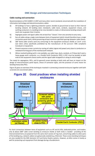
- 1. EMC Design and Interconnection Techniques Cable routing and connection Recommendations of IEC 61000‐5‐2:1997 and many other recent standards concerned with the installation of information technology and telecommunications cables: a) All buildings to have a lightning protection system, bonded at ground level at least to their internal bonding network. All building steel, metalwork, cable ducts, conduits, equipment chassis, and earthing conductors in a building to be cross‐bonded to create a 3‐dimensional bonding network with mesh size no greater than 4 metres. b) Segregate power and signal cables into at least four "classes", from very sensitive to very noisy. c) Run all cables along a single route between items of equipment (which should therefore have a single connection panel each), whilst preserving at least minimum specified spacings between cable classes. d) 360o Bond cable screens (and any armouring) to the equipment enclosure shields at both ends (see later) unless specifically prohibited by the manufacturer of the (proven EMC compliant) transducer or equipment. e) Prevent excessive screen currents by routing all cables (signal and power) very close to conductors or metalwork forming part of the meshed earth network. f) Where meshed building earth is not available, use cable trays, ducts, conduits, or if these don't exist a heavy gauge earth conductor, as a Parallel Earth Conductor (PEC). A PEC must be bonded at both ends to the equipment chassis earths and the signal cable strapped to it along its entire length. The needs for segregation, PECs, and (in general) screen bonding at both ends will have an impact on the design of interconnections panel layout, choice of connector types, and the provision of some means for bonding heavy‐duty PECs. Figure 2E gives an overview of the techniques involved in connecting screened enclosures together with both screened and unscreened cables. For short connections between items of equipment such as a PC and its VDU, dedicated printer, and modem, only d) above (360o cable screen bonding to enclosure shields at both ends) is needed ‐ providing all the interconnected items are powered from the same short section of ring main, and all long cables to other parts of the building (e.g. network cables) are galvanically isolated (e.g. Ethernet). These screen bonding techniques are also needed for the EMC domestic hi‐fi and home theatre systems. However, a) often comes in handy as well for protecting such equipment from damage during a thunderstorm.
- 2. 2.6 Getting the best from cables Open any signal cable manufacturer's catalogue and you will find a huge variety of cable types, even for similar tasks. This is a warning that cables are all imperfect. The best cable for a given application will be difficult to select, and then will probably be too expensive, too bulky, too stiff, and only available to special order on 26 week leadtime in 5km reels. 2.6.1 Transmission lines Transmission line techniques prevent cables from acting as resonant antennas. When the send and return conductors of a signal current loop are physically close together and so enjoy strong mutual coupling, the combination of their mutual capacitance and inductance results in a characteristic impedance Z0 = , where L and C are the capacitance and inductance per unit length (a fraction of the A of the highest frequency of concern). Z0 can be calculated for cables and connectors When Z0 is kept constant over the entire length of an interconnection, and when drive and/or send (source or load) impedances are "matched" to Z0, a controlled‐impedance transmission line is created and resonant effects do not happen. The intrinsic inductance and capacitance of the conductors also create far fewer problems. This is why RF and all EMC test equipment use 50Q transmission line cables and connectors (see Figure 2F), and why high‐speed and/or long distance data busses and serial communications also use transmission lines (usually in the range 50 to 120Q). Lines must be matched, and the classical method is to match at both source and load. This provides maximum power transfer from source to load, but as it results in a 50% voltage loss for each interconnection, it is often not used for normal signal interconnections in non‐RF equipment. Instead, transmission lines are often terminated at just one end, so as not to lose voltage, even though this is not ideal from either an EMC or signal integrity point of view. Terminating at one end only is a conscious decision to compromise on the engineering to save cost. Figures 2G, H, and J show the main termination methods.
- 4. But nothing is perfect and even though not resonant, even the best practical transmission lines still leak a bit. Installation also reduces transmission line performance by causing variations in Z0 (increasing leakage) when cables are bent sharply, crushed, strapped or clipped too tightly, repeatedly flexed, damaged, or fitted with inadequate connectors. Unfortunately, the overall cost of creating transmission line cable interconnections with high enough quality at modern high frequencies can be very high. Flexible cables for microwave test equipment, for instance, can cost hundreds of pounds per metre. This is why, for GHz Ethernet to run on low‐cost Cat 5 UTP (unscreened twisted pair), it has to use sophisticated DSP algorithms to reduce data rate and spread it randomly, and it still needs four pairs. So although transmission lines are very powerful, they are not a universal panacea for cable problems at high frequencies. 2.6.2 EMC considerations for conductors used inside and outside products Inside a product ‐ if the product's enclosure shields, and the screening and filtering of its external cables is good enough, almost any type of wire or cable can be used, although signal integrity will suffer. The problem here is that for high‐performance digital or analogue electronics the cost of the enclosure shielding and filtering required can be so high that it would have been cheaper to use more expensive internal cables. It is generally most cost‐effective to avoid all internal cables, keeping all non‐optical‐fibre signals in the tracks of plugged‐together PCBs (preferably a single PCB, even using flexi‐rigid types). To make this work the PCBs need to be designed according to the Part 5 of this series, using a ground plane under all tracks. This generally reduces the cost of enclosure shielding and filtering to give the most cost‐effective product, and because it also improves signal integrity it usually saves a couple of development iterations too. Outside a product ‐ unscreened cables with single‐ended signals are now a serious liability whether the product is digital or analogue. Filtering digital signals does not help much to reduce emissions: single‐ ended drive produces copious common‐mode currents at the signal frequencies themselves, causing the product to fail conducted or radiated emissions tests depending on signal frequency. Any filtering would need to remove the signal, which does not help. Filtering can work quite effectively for low‐frequency analogue signals, but for precision beyond ±0.05% (12 bits) the cost of the filter and its board area increases rapidly. Of course filters have difficulty
- 5. removing in‐band interference (such as powerline hum) that a properly designed balanced communication system would easily reject. 2.6.3 Pairing send and return conductors Even when not using transmission lines, always use paired conductors. Provide a dedicated return path for the return current as close as possible to the send path (and not via an earth or a screen). This works even when signals are single‐ended and all their return conductors are bonded to a common reference potential. The fluxcompensation effect encourages return currents to flow in the path nearest to the send conductor, in preference to alternative current paths, and we can use this natural phenomenon to help keep the field patterns of our cables tight and reduce their E and M leakages. Figure 2K shows the general principle, which is of universal application. Figure 2K Routing of the conductors in a cable (this example is of switched circuits, but the principle is universally applicable) It is bad practice to run the return path differently from send path ‐ always use paired send and return conductors which are physically close Figure 2K shows a mains supply with a switch in one line, but the same principle applies to signals. The closeness of the send and return conductors over the entire current loop is absolutely crucial at the highest frequencies for circuits to work at all, never mind good EMC. Ribbon cables carrying a number of single‐ended (i.e. 0V referenced) signals are very poor indeed for EMC and signal integrity, but screening them results in stiff, bulky, expensive cable assemblies which is what flat cables were supposed to avoid. Using the pairing technique for flat cables improves their EMC considerably and this conductor arrangement is the best: return, signal, return, signal, return, etc. A less effective alternative which is often recommended is: return, signal, signal, return, signal, signal, return, etc. Significant improvements can often be made by fitting flat cable ferrite clamps (common‐mode chokes) at the source end(s), so that the conductor pairs behave as if they were driven from a balanced source at high frequencies, although proper balanced drive/receive circuits are better (see Part 1 of this series). Twisted pairs are very much better than parallel pairs. Use twisted triples, quads, etc. where this is what it takes to get all the send and return paths of a signal in close proximity. Twisted send and return conductors are strongly recommended for power cables: combining all phase and neutral conductors (two for single‐phase, three for three‐phase, four for three‐phase plus neutral) in a single cable with a slow twist greatly reduces the emissions of powerline M field emissions. M fields from power busbars or individually routed phase and neutral cables can render whole areas of buildings unfit for CRT‐based VDU monitors.
- 6. Twisted pairs using balanced circuitry (see Part 1 of this series) and common‐mode chokes can be good for signals up to some tens of MHz, depending on the "balance" of the circuit, cable, and connectors. Any unbalance will convert some of the wanted signal into useless common‐mode currents, which all leaks away as fields. Just a few micro‐amps of common‐mode can fail an emissions test. Tighter and more precisely regular twists make cables better for higher frequencies. A great many types of twisted‐pair cables are available, some intended for transmission lines (Z0 will be specified). But twisted pair technology does not suit mass‐termination. So‐called "twist + flat" flat cable has multiple twisted pairs all formed into a ribbon, but has regular lengths of 100mm or so of parallel conductors for mass‐terminating connectors ‐ and the flat bits are so long they compromise EMC. 2.6.4 Getting the best from screened cables: the screen There is no such thing as a cable that "complies with the EMC Directive", there are only cables with frequency‐dependant screening performance. Cable screens must cover the entire route with 360o coverage. Making screening work effectively with low‐cost these days is increasingly difficult, except for the least aggressive and least sensitive signals. It is no longer best practice to use the shield of a cable as the signal return. The problem with co‐axial cables is that the screen carries currents for both the signal return and external interference, and they use the skin effect to keep them on different sides of the screen (known as "tri‐ axial mode"). This works fine for solid copper screens (plumbing, to you and me), but flexible screened cables aren't very good at keeping the two currents apart, so return currents leak out, and interfering currents leak in. But (I hear you say) all RF test equipment uses flexible co‐ax, so it must be OK. Look carefully at these cables next time you are in an EMC test lab: the cables used for higher frequencies are very thick, stiff, and expensive, partly because they are double‐screened at least. They use expensive screwed connectors (e.g. N‐types), and are always used in matched (at both ends) 50Q transmission lines. They are also treated reverentially and woe betide you if you tread on one. At higher frequencies than the average EMC test lab, semirigid or rigid co‐axial cables have to be used, as stiff as automotive brake pipes. The ability of a screened cable to prevent interference is measured in two ways, as shielding effectiveness (SE), and also as ZT. SE seems obvious enough, and ZT is simply the ratio of the voltage which appears on the centre conductor in response to an external RF current injected into the screen. For a high SE at a given frequency, we need a low ZT. A flat ZT of a few milliQ over the whole frequency range would be ideal. A very broad‐brush summary of the screening qualities of typical types of screened cables follows, but remember that within each broad category there are many different makes and grades with different performances: • Spiral wrapped foil is not terribly good at any frequency, and gets progressively worse > 1MHz. • Longitudinal foil wrap is better than spiral foil. • Single braid is better than foil at all frequencies, but still gets progressively worse > 10MHz. • Braid over foil, double braid, or triple braid, are all better than single braid and all start to get progressively worse >100MHz • Two or more insulated screens are better still, but only up to about 10MHz, at higher frequencies resonances between the screens can reduce their effectiveness to that of just one screen at some frequencies. • Solid copper screens (e.g. semi‐rigid, rigid, plumbing) are better than braid types and their screening performance continually improves at higher frequencies, unlike braid or foil, which always degrades above some frequency. Round metal conduit can be used to add a superb high‐frequency performance screen. (Armouring is also useful as a screen but only at low frequencies, say up to a few MHz.) • "Superscreened" cables use braid screens with a MuMetal or similar high‐permeability wrap. These can be as good or even better than a solid copper screen, whilst still retaining some flexibility, but are expensive and suit applications where performance is more important than price (e.g. aerospace, military). • I'm only aware of one manufacturer (Eupen) offering ferrite‐loaded screened cables, which may offer improved high‐frequency performance with good flexibility without the high cost of superscreened cables.
- 7. To reduce the bulk and cost of our screened cables and still get good EMC for highperformance modern products we need to use paired conductors for every signal and its return, preferably twisted pairs, just as described above for unscreened cables. Balanced drive/receive is also a great help. 2.6.5 Getting the best from screened cables: terminating the screen Using co‐axial cables and connecting their screens to a circuit 0V track is almost a guarantee of EMC disaster for high‐performance digital and analogue products, for both emissions and immunity. Insulated BNC connectors on a product are usually a sign that all may not be well for EMC. Cable screens should always be connected to their enclosure shield (even if they then go on to connect to circuit 0V), unless there are very good quantitative engineering and EMC reasons why not. "We've always done it this way" is not a reason. Circuit development benches need to create the real structure of the product and the real interconnections with the outside world as closely as possible. Otherwise circuit designers may use various interconnection tricks to make their PCBs test well on the bench (I know, I used to do it too) ‐ leaving it to someone else to sort out the resulting real‐life application and EMC problems. But even a high‐quality screened cable is no good if the connection of the screen to the product is deficient. Cable screens need to be terminated in 360o ‐ a complete circumferential connection to the skin of the screened enclosure they are penetrating, so the connectors used are very important. "Pigtails" should never be used, except where the screen is only needed up to a couple of MHz. Where pigtails are used they must be kept as short as assembly techniques allow, and splitting a pigtail into two on opposite sides also helps a bit. In the mid 1980's a company replaced all their pigtailed chassis‐mount BNCs with crimped types for EMC reasons. Although the crimping tool cost around £600 they were surprised to find they quickly saved money because crimping was quicker and suffered fewer rejects. So pigtailing may be uneconomic as well as poor for EMC. The "black magic" of cable screening is to understand that a cable's SE is compromised if its connectors, or the enclosure shields it is connected to, have a lower SE. It is possible to use screened cables successfully with some unshielded products, if they use no internal wires and their PCBs are completely ground‐planed with low‐profile components. This is because the PCB ground plane, like any metal sheet, creates a zone of reduced field strength ‐ a volumetric shield for a limited range of frequencies. Successful use of this technique depends upon the electronic technology in the product, and is unlikely to be adequate for high‐performance digital or analogue products. The cable screens would connect 360o to the PCB ground plane. 2.6.6 Terminating cable screens at both ends This seems like heresy to some, but with the high frequencies in use these days leaving an end unterminated will usually leak too much. Screen termination at both ends also allows the screen to work on all orientations of magnetic fields. Of course, connecting screens at both ends allows any earth potential differences to drive currents in the screen that might cause hum pickup, and even melt the cables. Where such earth currents exist it is an indication of poor facility earth‐bonding which could allow earth faults or thunderstorm surges to destroy inadequately protected electronics. It is not unknown for screened cables to flash‐over at unterminated ends during thunderstorms, creating obvious hazards. It is sometimes recommended to electrically bond a cable screen at one end, and terminate the other with a small capacitor. The aim is to prevent excessive power frequency screen currents, and it does work to some extent although it is difficult to get capacitors to provide low enough inductance for very high frequencies and it does nothing for surge and flashover problems. Insulated BNC connectors are available with screen‐to‐chassis capacitors built‐in, but the last price I had for types which worked well to 1GHz was nearly £20 each. Galvanically isolated communications offer a way out of bonding screens at both ends, but such an approach needs careful attention to detail, especially the safety and reliability issues associated with installation earth‐faults and surges. Metal‐free fibre optics are the best kind of galvanically‐isolated signal communications, and the easiest to use. Section 2.5 above briefly lists the currently accepted best installation practices in achieving good EMC (e.g. using a PEC to divert heavy earth currents) without suffering hot cables and without compromising safety. Refer to IEC 61000‐5‐2:1997 for more detail.
- 8. 2.7 Getting the best from connectors Connectors suffer from many of the same EMC problems as cables, after all, they are just short lengths of conductor in a rigid body. It is best to segregate connectors into those used for internal connections, and those used for outside connections, because of the possibility of flashover from outside to inside pins during surge or electrostatic discharge events. Such flashovers can bypass protective devices. 2.7.1 Unscreened connectors Controlled‐impedance transmission‐line connectors are increasingly available for high‐speed backplanes or cables. When not using transmission lines, much improved EMC and signal integrity can be had from ordinary multiway connectors (e.g. DIN41612, screw‐terminal strips) by making sure that each "send" pin has a return pin alongside. At the very least provide one return pin for every two signals. It is best when these are used with balanced signals, but the technique also helps when signals are single‐ended. 2.7.2 Connectors between PCBs Connectors between PCBs (e.g. daughterboard to motherboard) also benefit greatly from multiple 0V pins spread over their full length and width, and a similar arrangement of power pins also helps significantly. Optimum signal integrity and EMC is generally achieved (for signals sharing the same power rails) with a pin pattern that goes: The following pattern provides lower performance but is often adequate, and uses fewer pins: It is also best to extend the connector over the full length of the common edge between the two boards, and liberally sprinkle 0V and power connections over the full length. There is some evidence that random pin allocations may provide better performance by breaking up standing wave patterns. Additional grounds between sensitive and noisy signals can help be a barrier to crosstalk. We don't really like connectors on PCBs, and they should be avoided if possible (reliability will improve as a result) ‐ as mentioned earlier, single or flexi‐rigid PCBs with ground planes under all their tracks are better. Also: don't socket ICs (use field programmable PROMS). Each IC socket pin is a little antenna positioned right at the most vulnerable or noisy location possible. 2.7.3 Screened connectors There is no such thing as a connector that "complies with the EMC Directive", there are only connectors with frequency‐dependant screening performance. Screened cables must maintain 360o screen coverage over their whole length, including the backshells of their connectors at both ends. Connector backshells must make 360o electrical bonds to the enclosure shields they are mounted on, using iris springs or some other method. Saddle‐clamps seem to make adequate screen bonds for most purposes in rectangular connector backshells, but avoid the ones that need the screen to made into a pigtail, however short. Figure 2L shows a typical D‐type screen termination. Co‐axial and twinaxial screened cables benefit most from connectors with screwed metal backshells. These are better and more reliable at high frequencies than bayonet types (like BNC), which is why they are used on satellite TV convertor boxes. Multiway screened cables are also best used with round connectors with screwed backshells, but are often specified with rectangular connectors such as D‐types or larger. Making a 360o connection from cable screen to connector backshell, and from backshell to enclosure shield, seems a lot to ask of some connector manufacturers, so check this has been done effectively before committing to a particular make or type. Especially watch out for single (or long) springs, clips, and wires, when used to make a screen bond: these are just pigtails and will limit SE at high frequencies. Unfortunately, many industry‐standard connectors do not allow correct termination of cable shields (e.g. jack plugs, XLRs, phonos, and any number of proprietary connector models). Also unfortunately, connector systems are still being designed without adequate thought being given to the need for simple 360o cable screen termination (e.g. RJ45, USB). The overall SE of a connector will be compromised if used with an enclosure shield or cable with a lower SE. Figure 2M shows some of the important considerations when bonding connectors to shielded enclosures.
- 9. COMPONENT ASSEMBLY TECHNIQUES Component Selection: Resistor Types – Carbon Composition, Film type and Wire Wound Film type has more inductance that carbon resistors Resonance due to Inductance and Capacitance is the limiting factor for the use of a resistor at HF Capacitor Types – Ceramic, Tantalum, Mica, Mylar, etc.. Electrolytic capacitors have large series resistance above 25 KHz Mica or Ceramic is Preferred for HF At VHF Feed Through Capacitor is used Inductor Air Core Inductor act as a source of Radiated Emission Magnetic Core can pick more EMI Thus Crystal Oscilator replace Inductors in PCB’s The careful assembly of the PCB is as relevant for the final equipment reliability as the circuit design or PCB design and fabrication. When going through equipment failure statistics, this fact can easily be verified. Assembly techniques can vary widely from case to case. While small‐scale production is fully based on manual performance, automation plays an important role in high‐volume assembly, especially in countries where manual labour is a main cost factor. Assembly techniques also undergo changes in the course of time with the accumulation of experience and with the introduction of new component types. A review on assembly techniques can therefore give an account of the present state of the art. To fit the scope of this book, the emphasis will be laid more on smaller production volumes with manual assembly techniques.
- 10. T joint caus Adeq mini has diam holes Co T reten joint leads body appr perp Fig. comp avail purp will a to ta Polar show Whe emp diffe have tape Co Com comp dicta The guide s due to ed by me quate pre mise stre to be pl meters sho s or 0.7 m mponent The bend ntion of t . In no ca s; any str y (compo oximately endicular 21‐1 sho ponent a able for oses is su automatic ke care o rised 2‐le w the pola re large q loyed wit rent deg e usually t . mponent ponents a ponent si ated by sp elines giv mechani echanical ecautions ss on sold anned an ould at t mm for pla Lead Pre ing of the he compo ase should ress on th onent‐lead y two ti r to the bo ows a fe s well as easy but uggested cally give of hole pa ad compo arity symb quantities th a thro rees of s to be sup Mountin are basic ide is usu pecial des PREPARA ven here ical stres inputs b taken d der joints nd consid he maxim ated‐thro eparation e axial co onent on d any dam he compo d junctio mes the oard so th ew of the s on the t perfect in Fig. 21 2.54 mm tterns in onents (e bol on the s of board oughput o sophistica plied in b ng ally moun ually opp ign requi ATION AN have ma s on the but also t during the . The opt dered han mum be 0 ugh holes omponent the PCB mage to th onent lead n) has t lead dia hat any st e very c solder jo compone 1‐2. In th m or 0.1" a grid sys .g., electr e top, afte ds have to of thousa ation and belt form nted on o posite to rements. ND MOUN inly the joint. M thermal e e PCB de imum com nd in han 0.5 mm m s to give s t leads is while a m he compo ds where to be av ameter. tress on t ommon oint. Ther ent prepa is device, increased stem on th rolytic cap er mounti o be asse ands of c automat with both only one the majo NTING OF purpose echanica effects do esign stag mponent nd with more than still reliab done in minimum o nent or it they dire oided. T The bent he compo shortcom efore sui aration. A , a change d spacing he same d pacitors) ing, for ea mbled, au omponen tion. For h the lead side of th or conduc COMPON to minim l stress o o lead to ge can b preparati the PCB n the lea ble solder a manner of stress ts leads b ectly com he lead t leads onent‐lea mings whi itable be A simple e from on between dimension have thei asy reada utomatic nts per h small eq d‐ends st he board. ctor patt NENTS mise the c on a sold the same be an eff ion as we design. d diamet joints. r to guara is introdu e caused e out fro bending‐ should fi d junction ich provi nding too hand‐hel ne bendin the bent nal base. r leads be bility. lead ben our. They quipment, icking on . In doub ern side, cracking der joint e stress s fective re ell as the m In any ca ter for no antee an uced on t while be om the co ‐radius sh it into t n is minim de stress ols must d device ng slot to t compon ent in a m ding mac y are ava , the com strips of le‐sided P unless o of solder is mostly situation. emedy to mounting ase, hole on‐plated optimum he solder nding the omponent hould be he holes mised. s on the be made for such the next ent leads manner to hines are ailable in mponents adhesive PCBs, the otherwise r y . o g e d m r e t e s e e h t s o e n s e e e
- 11. No code orient direct Th transis is not Fi A) lifting resisto surfac junctio mater sealed certai extend holes the bo onpolaris the same tation can ions must he uniform stors, ICs only for a igures 21 ) Horizon of solde or body. ce to avo on due t ials. Whe d compon n distanc ded to a where th oard are r C ed 2‐lead e orientati n be both t be main mity in or , etc.) is d assembly .4 gives a tally‐mou er joints B) Vertica id strain to differe ere necess nents too ce from certain e solder f recommen Component orie d compone ons throu horizont tained. rientation determine convenie few mor unted res along wit ally‐moun on the s ent therm sary, resil o, have to the boar length al flows up nded. entation to be ke ents are m ughout th tal as wel n of polar ed during ence but a e mountin istors mu th the co nted resis older join mal expan lient spac o be mou rd becau ong the in the ho ept uniform mounted he board l as verti rised com g the desig also later ng details ust touch opper pat tors shou nt as wel nsion coe cers have unted in se the i leads. Es le, clean to give th (Fig. 21‐ cal but u mponents gn of the during te s for 2‐lea the boa ttern und uld not be ll as on t efficients to be pro such a w nsulation pecially w leads of a he markin ‐3). The c niformity (diodes, PCB. Its i sting or s ad compo rd surfac der pressu e flush to the comp of lead ovided. C) way as to coating with plat at least 1 g or colo compone in readin capacitor importanc servicing. nents: ce to avo ure on th o the boa ponent‐lea and boa ) Coated o o provide is usual ed‐throug mm abov ur nt ng rs, ce id he rd ad rd or a lly gh ve
- 12. Some dissipa surfac better condu suitab board finishe could Tr give c more mo ating mo ce. This is r air flow ctors, th bly strippe mounte ed PCB is be harmf ransistor onsiderab ounting re re heat t to minim for coolin he jumpe ed back so d compo recomme ful to the mounting ble stress ecommen than 1 W mise therm ng of the r wire m o as not t onents ov ended to electrical g should s on the s ndations a W should mal stress compone must be o affect t ver cond prevent t l function never be solder joi are given be clearl s on the l ent. B) W insulated he solder uctors, a the forma ning of the done flu nts and t in Fig. 2 y separat aminate here jump . The in ring. C) In a conform ation of m e circuit. ush to th to the lea 1‐5 A:. Co ted from but also t per wires sulation the case mal coati moisture t e board: ad junctio omponen the boa to enable cross ov has to b of flush t ing of th traps whic This cou ons beside ts rd a er be to he ch ld es
- 13. the po wide r the us case) washe M integr to be packag M compo and vi surviv clamp St mount solder simple Straig provid to hol Th prope solder solder compo impro rule, t but it Lead clinch offset used a achiev mainta ossible ov range of r se of slee have to b ers are pre Mounting o ated circu readjuste ge type. Mechanical onent we brations e the tran s and bra traight‐thro ting of c ring techn e since th ht‐throug des an opt d the com he clinchi r position ring fram ring and t onent. In ved due the clinch is an acce preformin ing is giv ‐ and dim as well. A ved whil ained. In verheatin resilient s eves is a be mechan eferably u of integra uits in TO ed. Simple securing ight is m in the ord nsport an ckets are ough mou componen niques. Th hey can b gh moun timum 36 mponent f ng of lead n for sold mes. Also the more addition to the la ed lead p epted pra ng: A co ven with mple lead A good co e the a addition, g during spacers an lso a com nically se used as in ated circuit O‐can or d e jigs are of comp ore than dinary use nd shipme available unting or nts (Fig. he replaci be readily ting is 60° symm firmly in i ds means ering. But o, hole‐t e the clea n, plated‐ arger wet portion sh ctice to e ompromis appropri preforma omponen advantage the lead the solde nd spread mmon pra cured to t ndicated i ts: To en ual‐inline available onents m 10 g. Thi e of the e ent handli e in a wid r lead cli 21‐7) is ng of stra y remove preferred etrical so ts positio s an addit t clinchin o‐lead c arance, th ‐through ted area hould not extend it f e betwe iate com ations are t retentio es of s s are cut Not Reco ering ope ders avail actice. If the board n Fig. 21 able an e‐package e for this must be c is is not o electronic ng prior t e variety inching: T compatib aight‐thro ed after h d for sin lder joint on while s tional ope g avoids t learance he easier hole sol and bett be exten further al een strai ponent le e shown i on on the traight‐th to final l mmended ration (F able. Wit large tra d, spacers 6 C. easy inse e (DIP), th purpose, considere only to w c equipme to the fin for such The simp ble with ough mou heating u ngle‐sided t. A drawb oldering eration af the need become will be t der conn ter mecha nded beyo ong cond ght‐throu ead prefo n Fig. 21‐ e board p hrough m ength in t ig. 21‐6). h single‐s ansistors s, washer ertion, th e leads h , for each ed as so withstand ent later, al use. Sp purposes le straig the com unted com p the so d PCBs b back is th it. fter the le for speci es less c the insert nection re anical con ond the a uctor tra ugh mou orming. T ‐8. Other prior to s mounting the same Recommende There is sided PCB (e.g., TO and sprin he leads ave usual h particul on as th the shoc but also t pecial clip . ght‐throug mmon ma mponents lder joint because e necessi eads are al pressu critical fo tion of th eliability ntact. As nnular rin cks. unting an The dimp shapes a soldering are st operatio ed a Bs, ‐3 ng of lly ar he ks to ps, gh ss is ts. it ty in re or he is a ng nd ple re is till n.
- 14. Theref popula GUILD Decou INTROD As muc rely he proble design determ design choice making Unfort Some g and ot always genera The gu over t compa in boo anothe types o The lo were o elimina inadve catego THE TO While in the proble Somet comply 1. Mini Althou well as Minim do to circuit and en source 2. Don I/O con or off f will ea emissio circuitr by exte on ano fore, lead ar with bu DLINES Fo upling DUCTION ch as we h eavily on d ms. Of co feature v mine whet guideline s without g design tr tunately, th guidelines thers have s be applie al. uidelines p he past y anies that w ks, magazi er and ma of boards. nger list w out‐dated ated, were ertently m ories: comp OP FOUR any rankin opinion of ms are the imes desig y with less imize signa ugh digital s voltage. izing signa prevent en board des nsure that e. 't locate ci nnectors g from the b sily drive o ons specifi ry is locate ernal sourc other. Circu d preform ulk electr r PCB Des hate to adm design guid urse, a go violates a g her or not es serve a stopping ade‐offs a here are n are based e no know ed. Others resented h year. The we work w nes and o ny of them was shorte or could e guideline ake things ponent pla ng of EMC f the autho e direct res gners are important al current designers Signal cur al current l nergy in th signers sho a low imp ircuitry be generally re board. High one cable ications [1 ed above a ces are ver uitry locate ming with onic equi sign – Com mit it, EMC delines wh od engine guideline, t the viola s a startin to analyz nd they he early as m d on circuit n origin. A s apply on here were longer list with here a n the web m are out ened by eli not be a es that co s worse. T cement, tr design gu or, deserv sult of boa aware of t guideline loop areas don't alw rrents alw loop areas he signal f ould always pedance p tween con epresent t hspeed circ relative to ]. This will a solid sign ry likely to ed betwee h semi‐au pment m mponent C engineers hen design er does no a more th tion is like ng point. ze every d elp to iden many design t or radiati A few guid ly to spec selected f t contains t the unive . In the lon t of date o iminating applied to ould easily The rema race routin idelines is e special a ard designs these gui es. s ays realize ays return s is perhap from coup s keep trac ath is prov nnectors the best po cuitry betw o the othe be true ev nal return flow onto en two cab tomatic e anufactur Placemen s and print ing or eva ot rely sol horough a ely to pres They help decision. D tify potent n guideline on models delines are cific situati from a mu s guideline ersity. It al nger list, g or applicab all the gui o a wide be misint ining guid ng, board d subjective attention. A s that viola delines, b e this, all e n to their s the singl ling to oth ck of wher vided to re ossible wa ween two c er with eno ven if the plane. Tra a board o le connect equipmen rers. nt, Trace R ted circuit luating PC ely on gui nalysis is sent a pro p the des Design guid tial proble es as there s, some are e very imp ons and a ch longer es contribu lso include uidelines o ble only to idelines th variety of terpreted elines we decoupling e, there ar A significa ate one of ut violate electrical s source (i.e le most im her circuits re the signa eturn ever y for ener connector ough volta cables are nsients an on one cab tions is mo nt has be Routing a board (PC CBs or diag delines. If normally c blem. Idea igner to m delines pla m areas. e are desig e based on ortant and are not ap list that w uted by s es guideline often confl o certain v hat didn't m f board d causing a ere groupe g and the to e four guid nt percent these fou them in ignals hav e. they flo mportant th s or radiat al currents ry signal c gy to be c s with atta ge to exce e well shiel nd RF curre le and off o ore difficult ecome ve and CB) designe gnosing EM a particul called for ally PCB EM make layo ay a role n enginee n experien d can near ppropriate was compile ome of th es publishe lict with on very specif make sens esigns. Al designer ed into fo op four. delines tha tage of EM r guideline an effort ve current w in loop hing you ca ting. Printe s are flowin urrent to oupled on ached cabl eed radiate ded and th ents induce of the boa t to protec ry ers MC lar to MI out in rs. ce rly in ed he ed ne fic se, so to our at, MC es. to as s). an ed ng its to es ed he ed rd ct.
- 15. 3. Control transition times in digital signals It is not uncommon to see products fail to meet emissions requirements at frequencies that are 10 ‐ 100 times the fundamental clock frequency. However, by controlling the rise‐ and fall‐times of the signal, it is possible to attenuate these upper harmonics significantly without degrading the signal quality or bit error rate. Signal transition times are readily controlled by choosing logic families that are appropriate to the task or (for capacitive loads) by putting a resistance in series with the source. 4. Provide a solid (not gapped) signal return plane This rule is essentially a corollary to the first rule, but it deserves special mention. Radiated EMI problems often result when well meaning designers cut a gap in a signal return plane forcing high‐frequency currents to find their way back to the source by high‐impedance paths. Often the gap is created in an attempt to avoid a perceived susceptibility problem. Although there are a few circumstances where a gap in the plane is called for, this is a decision that should be part of a well thought‐out plan. Solid return planes should never be gapped just to comply with a guideline or an application note. GUIDELINES FOR COMPONENT PLACEMENT • Connectors should be located on one edge or on one corner of a board. The purpose of this guideline is to make is easier to comply with Guideline #2 above. • A device on the board that communicates with a device off the board through a connector should be located as close as possible to that connector. • Components not connected to an I/O net should be located at least 2 cm away from I/O nets and connectors. I/O lines represent one of the easiest ways to couple unwanted energy on or off the board. • All off‐board communication from a single device should be routed through the same connector. This is to prevent radiated emission and susceptibility problems as described under Guideline #2 above. • Clock drivers should be located adjacent to clock oscillators. This is consistent with the idea of minimizing loop areas (see Guideline #1 above). GUIDELINES FOR TRACE ROUTING • All power planes and traces should be routed on the same layer. This helps prevent unwanted noise coupling between power buses. It usually results in an efficient layout, since no two devices require the same power at the same point and devices using the same power bus are generally grouped. • Critical signal traces should be buried between power/ground planes. Signals on traces between solid planes are less likely to interact with external sources or antennas. • No trace unrelated to I/O should be located between an I/O connector and the device(s) sending and receiving signals using that connector. • Signals with high‐frequency content should not be routed beneath components used for board I/O. I/O lines represent one of the easiest ways to couple unwanted energy on or off the board. • Critical nets between planes should be routed at least 2 mm away from the board edge. Signals on traces very close to the board edge are more easily coupled onto and off from the board. • On a board with power and ground planes, no traces should be used to connect to power or ground. Connections should be made using a via adjacent to the power or ground pad of the component. Traces take up space on the board and increase the inductance of the connection. • On boards with multiple signal return planes, all vias connected to one signal return plane should also connect to the others. Attempts to control the flow of signal return currents by connecting to different planes usually create more problems than they solve. It is generally desirable to have all return planes in a PCB at the same potential. They should be shorted together at every opportunity.
- 16. The trace width formulas are: I = 0.0150 x dT 0.5453 x A0.7349 for internal traces I = 0.0647 x dT0.4281 x A0.6732 for external traces where: I = maximum current in Amps dT = temperature rise above ambient in °C A = cross‐sectional area in mils² GUIDELINES FOR BOARD‐LEVEL DECOUPLING Due to unwanted coupling of Power Sources with subsystems, High Speed Switching transience Occur. Decoupling is the process of preventing undesired coupling between subsystems via the power supply connections. A Capacitor is placed in Shunt to the Power Source (or the Source that may couple) which will absorb the transient current.
- 17. 1.1 Boards with closely spaced planes • On boards with closely spaced (i.e. less than 0.25 mm) power and ground planes, the location of decoupling capacitors is not nearly as important as the inductance associated with their connection to the planes • Decoupling capacitors should be connected directly to power/ground planes using vias in or adjacent to the pads. • It is unnecessary and ineffective to use capacitors with a nominal value that is less than the board's interplane capacitance. At low frequencies, higher values of ca‐ pacitance are desirable. At high frequencies, connection inductance is much more important than the nominal value of the capacitor. • Power supply leads from active devices and decoupling capacitors should be connected directly to the power and ground planes. No attempt should be made to connect chip leads directly to a decoupling capacitor. 1.2 Boards with widely spaced planes • On boards with widely spaced (i.e. greater than 0.5 mm) power and ground planes, a local decoupling capacitor should be located near each active device. If the active device is mounted on the side of the board nearest the ground plane, the decoupling capacitor should be located near the power pin. If the active device is mounted on the side of the board nearest the power plane, the decoupling capacitor should be located near the ground pin { • Decoupling capacitors should be connected directly to power/ground planes using vias in or adjacent to the pads. Decoupling capacitors can share a power or ground via with the active device if this can be accomplished without traces (or with a traces length less than the power/ground plane spacing). • It is unnecessary and ineffective to use capacitors with a nominal value that is less than the board's interplane capacitance. At low frequencies, higher values of ca‐ pacitance are desirable. At high frequencies, connection inductance is much more important than the nominal value of the capacitor. 1.3 Boards with no power plane • On boards with no power plane, a local decoupling capacitor should be located near each active device. The inductance of the decoupling capacitor connection between power and ground should be minimized. Two local decoupling capacitors with a few centimeters of space between them, can be used to provide more ef‐ fective decoupling than a single capacitor Board Zoning Board zoning has the same basic meaning as board floor planning, which is the process of defining the general location of components on the blank PCB before drawing in any traces. Board zoning goes a little bit further in that it includes the process of placing like functions on a board in the same general area, as opposed to mixing them together (see Figure 10). High‐speed logic, including micros, are placed close to the power supply, with slower components located farther away, and analog components even farther still. With this arrangement, the high‐speed logic has less chance to pollute other signal traces. It is especially important that oscillator tank loops be located away from analog circuits, low‐speed signals, and connectors. This applies both to the board, and the space inside the box containing the board. Do not design in cable assemblies that fold over the oscillator or the microcomputer after final assembly, because they can pick up noise and carry it elsewhere.
- 22. Imp Chara Trans termina delay. T transmi betwee This i wavefo notably charact interest normall The g It can positive Reactan Co Since charact but with (with th the line charact purely b length, The b shapes. solution best be approxi conditio Fortu of inter commo (trace o sandwic The fa (other t the rea input m pedance acteristic mission lin ating imped This delay ssion line n 0.4 and 0 s to say th rm. The v y that the eristic imp t. These tw ly used in d eneral cas n be show e square r nce per un the two eristic imp h the pecu he delay as e. Another eristic imp by static m which in tu bad news Only a ns. If an ac et are the mations a ons impose nately, the rest. We w n structur over a diel ched betw act that th than the de lm of digit makes its w e Contr impedan ne correct dance was y is the tim and this s 0.9. hat for a c validity of e losses in pedance is wo approx digital desi e of Capac wn that fo root of th it of length reactances pedance is uliarity tha s mentione conseque pedance i means. Tho urn depen is that the handful o ccurate im e numeric applied to ed by the g ere are app will here co res in PCB ectric ove een two g he transmi elay pheno tal design ay to the o ol nce of a tr ly termina s present t me that t speed is a correctly t these as n the tra essentiall ximations igns, so we citive React r a line w he produc h. s are imag s a real nu at it does n ed above) ence, show s essentia ose means d strictly o ere are no of cases w mpedance c cal metho some dec geometry ( proximate oncentrate B design. T r a ground round plan ssion line omenon) is . As result output wit ransmissi ated at on there, with akes the fraction o terminated sertions is nsmission y indepen are justifie e can confi tance and without los ct of the ginary num mber. In o not dissipa at the oth wn in the t ally a dyna depend o of the geom o practical with simpl calculation ods. These ceptively s (metal and or accurat e of some These are d plane) an nes). acts as if t s the reaso t of its ow hout reflec on line e end beh h the only electrical of the spe d line will s limited line itse dent of th ed in the idently use Inductive sses, the c Inductive mbers of o other wor ate power er end by third expr amic phen f the indu metry of th general e e geomet n is needed e methods simple equ d dielectric te enough of those c variations nd "striplin the load w on why we wn nature, ctions or d haves at th noticeable phenomen eed of ligh be no ref by some lf are neg he frequen typical sit e the result and React characteris Reactance opposite s ds, it look . In fact th the real re ression, is nomenon, ctance and he line in q xpressions try that a d for an a s work by uations sa c). solutions cases, esp s of the ub ne" (trace was directl e are intere the wave istortions he other e e effect bei na to trav ht in vacuu lections di implicit a gligible an ncy in the uations an ts presente ance is: stic imped e and the ign it resu ks as a reg he power i esistor that that even it can be d capacita uestion. s applicabl dmit exac rbitrary ge y successi tisfying th for a num ecially as biquitous buried in y present ested in its eform pres of any kind end as if th ing a certa vel over th um, typica istorting th assumption nd that th spectrum nd materia ed in here dance is th e Capacitiv ults that th ular resist is dissipate t terminat though th e calculate nce per un le to all lin ct analytic eometry th ive numer he bounda mber of cas it applies "microstri a dielectr at the inp s behavior sented at d. he ain he lly he ns, he of als . he ve he tor ed es he ed nit ne cal he ric ary es to p" ic, put in its
- 23. Some of the Jargon and Background Core Construction: PCB fabrication process that piles up core materials with intermediate prepeg material. This method always results in an even number of layers. Foil construction: PCB fabrication process similar to the Core Construction except in the external layers. The external layers are added using sheets of copper foil on top of prepeg material. Even though this method can theoretically produce odd number of layers it is recommended to still use an even number due to the risk of warpage and cost (it is usually cheaper to add a layer). Prepeg: Short for pre‐impregnated material. It consists of sheets of the basic material (for example, FR4) impregnated with a synthetic resin partially cured to an intermediate stage. Prepeg is used between sheets of core material for middle layers and with copper foil on top for external layers. Copper Clad or "Core Material":: It is one of the raw materials used by PCB fab houses. It consists of a layer of dielectric material (the most common is FR4) sandwiched between layers of copper on each face. The copper layers are generally of the same thickness. The copper thickness is usually expressed in terms of "oz.", or more correctly in "ounces per square foot". This unit is equivalent to 1.4‐mil thickness (35 microns). Most digital circuit designs use substrates of a glass/epoxy composite known as FR‐4. Commonly commercially available values of copper thickness are 0.5, 1, 2 & 3 oz. FR4: Typical material used in digital design. FR4 is a glass fiber epoxy laminate. It is the most commonly used PCB material. "FR" stands for "Fire Retardant" (ANSI). It is usable up to frequencies in the order of 1 GHz, with losses increasing with the frequency. In digital designs, the losses are not that bad. In fact, the low Q (high loss) materials are preferred for these applications because thy help to dissipate the energy of reflections and other spurious distortions. Padstack: The description of copper and dielectric layers constituting a PCB, specifying each thickness. It consists of a number of pre‐peg, cores and copper layers. Since the optimum padstack is PCB fab technology dependent, it is always a good idea to check a proposed padstack with your PCB house. Microstrip: Consists of a trace running on the surface of a PCB separated by one or more layers of dielectric material from a ground plane located underneath. It is also called "surface microstrip" to distinguish it from the "coated" or "embedded" variations. Embedded Microstrip: Similar to the plain or "surface microstrip" but buried into the dielectric material. Coated Microstrip: Similar to the "embedded microstrip", differing from it because of the dielectric thinness on top and the construction process. The dielectric on top is usually the solder mask coating the PCB surface. It is an extreme case of Embedded Microstrip with different dielectric constant than the material below. The impedance does not usually change significantly from the regular Microstrip case except in case of very thin traces, which change a few units percent. Stripline: Trace running between two ground planes. See under the "symmetric" and "asymmetric" variations. Symmetric Stripline: This geometry consists of a trace running between two ground planes located in layers above and below with the same dielectric thickness and material on both sides. Asymmetric Stripline: Similar to the symmetric stripline except that the dielectric thickness above and below the trace are different. The material is typically of the same kind. Etching: Chemical process to remove the unwanted copper from a layer during the fab process. The copper face where the etching solution is applied results in extra etching compared with the copper layer facing the FR4 core. This effect may be important in case of very thick copper or very narrow traces. Ground Plane: For the purpose of impedance control a well decoupled VCC plane is equivalent to a true
- 27. Note: If Mother Board Design Question is asked, write about all the PCB Design techniques viz., Trace Routing, Impedance Control, Zoning etc.. Centric with Mother Board. There is no Special Technique for Mother Board Design, but it will be done with more Precaution. Present the Answer Accordingly.